SGM58031
Ultra-Small, Low-Power, 16-Bit
Analog-to-Digital Converter with Internal Reference
GENERAL DESCRIPTION
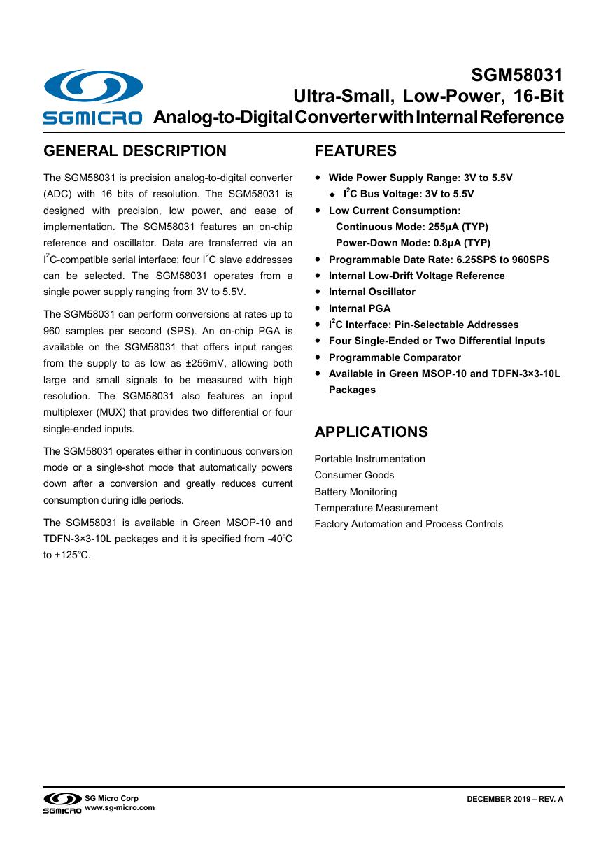
The SGM58031 is precision analog-to-digital converter
(ADC) with 16 bits of resolution. The SGM58031 is
designed with precision, low power, and ease of
implementation. The SGM58031 features an on-chip
reference and oscillator. Data are transferred via an
I2C-compatible serial interface; four I2C slave addresses
can be selected. The SGM58031 operates from a
single power supply ranging from 3V to 5.5V.
The SGM58031 can perform conversions at rates up to
960 samples per second (SPS). An on-chip PGA is
available on the SGM58031 that offers input ranges
from the supply to as low as ±256mV, allowing both
large and small signals to be measured with high
resolution. The SGM58031 also features an input
multiplexer (MUX) that provides two differential or four
single-ended inputs.
The SGM58031 operates either in continuous conversion
mode or a single-shot mode that automatically powers
down after a conversion and greatly reduces current
consumption during idle periods.
The SGM58031 is available in Green MSOP-10 and
TDFN-3×3-10L packages and it is specified from -40℃
to +125℃.
FEATURES
● Wide Power Supply Range: 3V to 5.5V
I2C Bus Voltage: 3V to 5.5V
● Low Current Consumption:
Continuous Mode: 255μA (TYP)
Power-Down Mode: 0.8μA (TYP)
● Programmable Date Rate: 6.25SPS to 960SPS
● Internal Low-Drift Voltage Reference
● Internal Oscillator
● Internal PGA
● I2C Interface: Pin-Selectable Addresses
● Four Single-Ended or Two Differential Inputs
● Programmable Comparator
● Available in Green MSOP-10 and TDFN-3×3-10L
Packages
APPLICATIONS
Portable Instrumentation
Consumer Goods
Battery Monitoring
Temperature Measurement
Factory Automation and Process Controls
SG Micro Corp
www.sg-micro.com
DECEMBER 2019 – REV. A
�
Ultra-Small, Low-Power, 16-Bit
Analog-to-Digital Converter with Internal Reference
SGM58031
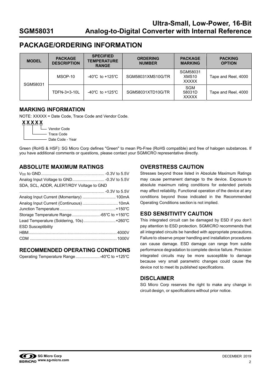
PACKAGE/ORDERING INFORMATION
MODEL
PACKAGE
DESCRIPTION
SPECIFIED
TEMPERATURE
RANGE
ORDERING
NUMBER
MSOP-10
-40℃ to +125℃
SGM58031XMS10G/TR
SGM58031
TDFN-3×3-10L
-40℃ to +125℃
SGM58031XTD10G/TR
MARKING INFORMATION
NOTE: XXXXX = Date Code, Trace Code and Vendor Code.
X
XXX X
Vendor Code
Trace Code
Date Code - Year
PACKAGE
MARKING
SGM58031
XMS10
XXXXX
SGM
58031D
XXXXX
PACKING
OPTION
Tape and Reel, 4000
Tape and Reel, 4000
OVERSTRESS CAUTION
Stresses beyond those listed in Absolute Maximum Ratings
may cause permanent damage to the device. Exposure to
absolute maximum rating conditions for extended periods
may affect reliability. Functional operation of the device at any
conditions beyond those indicated in the Recommended
Operating Conditions section is not implied.
Green (RoHS & HSF): SG Micro Corp defines "Green" to mean Pb-Free (RoHS compatible) and free of halogen substances. If
you have additional comments or questions, please contact your SGMICRO representative directly.
ABSOLUTE MAXIMUM RATINGS
VDD to GND ....................................................... -0.3V to 5.5V
Analog Input Voltage to GND ............................ -0.3V to 5.5V
SDA, SCL, ADDR, ALERT/RDY Voltage to GND
.......................................................................... -0.3V to 5.5V
Analog Input Current (Momentary) ............................. 100mA
Analog Input Current (Continuous) ............................... 10mA
Junction Temperature ................................................. +150℃
Storage Temperature Range ........................ -65℃ to +150℃
Lead Temperature (Soldering, 10s) ............................ +260℃
ESD Susceptibility
HBM ............................................................................. 4000V
CDM ............................................................................ 1000V
RECOMMENDED OPERATING CONDITIONS
Operating Temperature Range ..................... -40℃ to +125℃
ESD SENSITIVITY CAUTION
This integrated circuit can be damaged by ESD if you don’t
pay attention to ESD protection. SGMICRO recommends that
all integrated circuits be handled with appropriate precautions.
Failure to observe proper handling and installation procedures
can cause damage. ESD damage can range from subtle
performance degradation to complete device failure. Precision
integrated circuits may be more susceptible to damage
because very small parametric changes could cause the
device not to meet its published specifications.
DISCLAIMER
SG Micro Corp reserves the right to make any change in
circuit design, or specifications without prior notice.
SG Micro Corp
www.sg-micro.com
DECEMBER 2019
2
�
Ultra-Small, Low-Power, 16-Bit
Analog-to-Digital Converter with Internal Reference
SGM58031
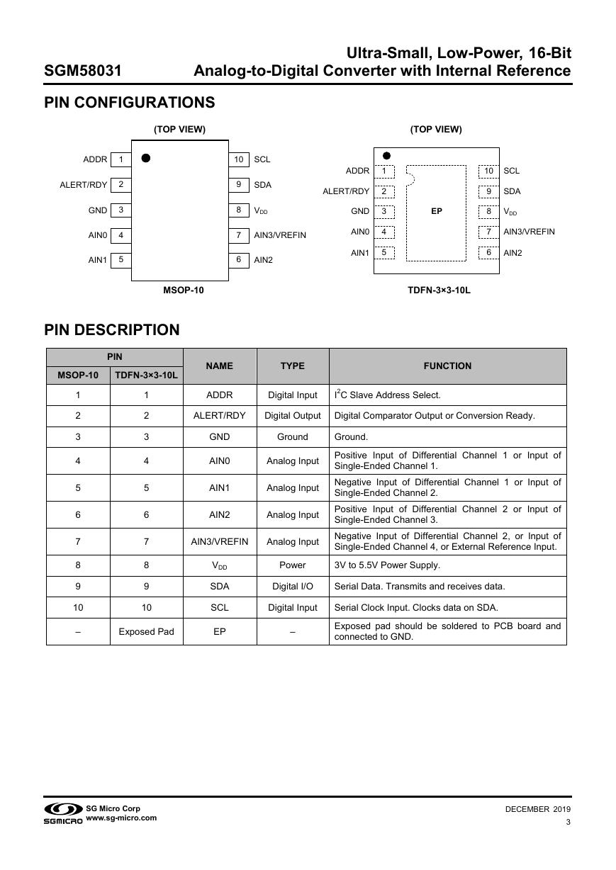
PIN CONFIGURATIONS
(TOP VIEW)
(TOP VIEW)
ADDR
ALERT/RDY
GND
AIN0
AIN1
1
2
3
4
5
MSOP-10
PIN DESCRIPTION
10
SCL
9
8
7
6
SDA
VDD
AIN3/VREFIN
AIN2
ADDR
ALERT/RDY
GND
AIN0
AIN1
1
2
3
4
5
10
SCL
9
8
7
6
SDA
VDD
AIN3/VREFIN
AIN2
EP
TDFN-3×3-10L
PIN
MSOP-10
TDFN-3×3-10L
1
2
3
4
5
6
7
8
9
10
Exposed Pad
1
2
3
4
5
6
7
8
9
10
‒
NAME
ADDR
TYPE
FUNCTION
Digital Input
I2C Slave Address Select.
ALERT/RDY
Digital Output Digital Comparator Output or Conversion Ready.
Ground
Ground.
Positive Input of Differential Channel 1 or Input of
Single-Ended Channel 1.
Analog Input
Analog Input Negative Input of Differential Channel 1 or Input of
Single-Ended Channel 2.
Positive Input of Differential Channel 2 or Input of
Single-Ended Channel 3.
Analog Input
Analog Input Negative Input of Differential Channel 2, or Input of
Single-Ended Channel 4, or External Reference Input.
3V to 5.5V Power Supply.
Power
Digital I/O
Serial Data. Transmits and receives data.
Digital Input
‒
Serial Clock Input. Clocks data on SDA.
Exposed pad should be soldered to PCB board and
connected to GND.
GND
AIN0
AIN1
AIN2
AIN3/VREFIN
VDD
SDA
SCL
EP
SG Micro Corp
www.sg-micro.com
DECEMBER 2019
3
�
Ultra-Small, Low-Power, 16-Bit
Analog-to-Digital Converter with Internal Reference
SGM58031
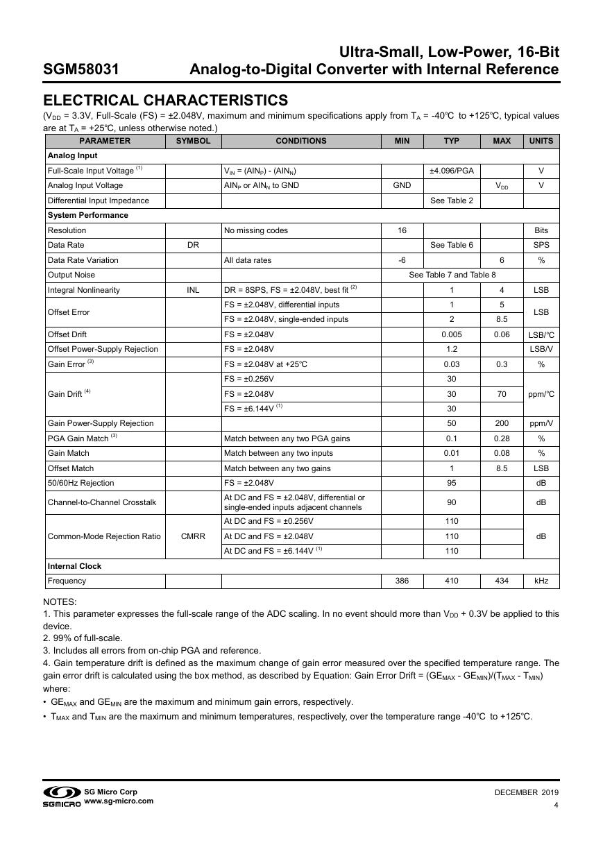
ELECTRICAL CHARACTERISTICS
(VDD = 3.3V, Full-Scale (FS) = ±2.048V, maximum and minimum specifications apply from TA = -40℃ to +125℃, typical values
are at TA = +25℃, unless otherwise noted.)
PARAMETER
SYMBOL
CONDITIONS
MIN
TYP
MAX
UNITS
Analog Input
Full-Scale Input Voltage (1)
Analog Input Voltage
Differential Input Impedance
System Performance
Resolution
Data Rate
Data Rate Variation
Output Noise
Integral Nonlinearity
Offset Error
Offset Drift
Offset Power-Supply Rejection
Gain Error (3)
Gain Drift (4)
Gain Power-Supply Rejection
PGA Gain Match (3)
Gain Match
Offset Match
50/60Hz Rejection
Channel-to-Channel Crosstalk
DR
INL
Common-Mode Rejection Ratio
CMRR
VIN = (AINP) - (AINN)
AINP or AINN to GND
No missing codes
All data rates
DR = 8SPS, FS = ±2.048V, best fit (2)
FS = ±2.048V, differential inputs
FS = ±2.048V, single-ended inputs
FS = ±2.048V
FS = ±2.048V
FS = ±2.048V at +25℃
FS = ±0.256V
FS = ±2.048V
FS = ±6.144V (1)
Match between any two PGA gains
Match between any two inputs
Match between any two gains
FS = ±2.048V
At DC and FS = ±2.048V, differential or
single-ended inputs adjacent channels
At DC and FS = ±0.256V
At DC and FS = ±2.048V
At DC and FS = ±6.144V (1)
1
1
2
0.005
1.2
0.03
30
30
30
50
0.1
0.01
1
95
90
110
110
110
410
GND
±4.096/PGA
See Table 2
16
-6
See Table 6
VDD
6
See Table 7 and Table 8
V
V
Bits
SPS
%
LSB
LSB
LSB/℃
LSB/V
%
ppm/℃
ppm/V
%
%
LSB
dB
dB
dB
4
5
8.5
0.06
0.3
70
200
0.28
0.08
8.5
Internal Clock
Frequency
386
434
kHz
NOTES:
1. This parameter expresses the full-scale range of the ADC scaling. In no event should more than VDD + 0.3V be applied to this
device.
2. 99% of full-scale.
3. Includes all errors from on-chip PGA and reference.
4. Gain temperature drift is defined as the maximum change of gain error measured over the specified temperature range. The
gain error drift is calculated using the box method, as described by Equation: Gain Error Drift = (GEMAX - GEMIN)/(TMAX - TMIN)
where:
• GEMAX and GEMIN are the maximum and minimum gain errors, respectively.
• TMAX and TMIN are the maximum and minimum temperatures, respectively, over the temperature range -40℃ to +125℃.
SG Micro Corp
www.sg-micro.com
DECEMBER 2019
4
�
Ultra-Small, Low-Power, 16-Bit
Analog-to-Digital Converter with Internal Reference
SGM58031
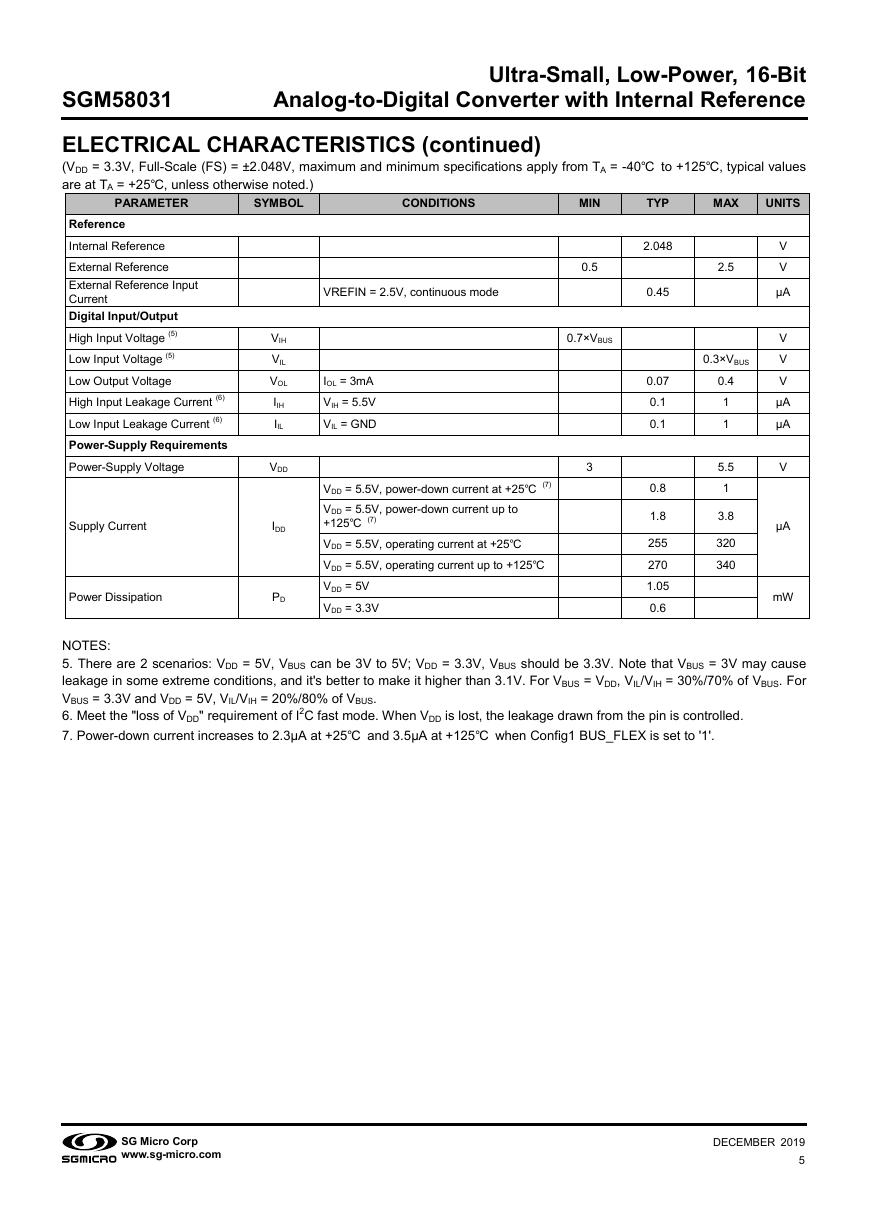
ELECTRICAL CHARACTERISTICS (continued)
(VDD = 3.3V, Full-Scale (FS) = ±2.048V, maximum and minimum specifications apply from TA = -40℃ to +125℃, typical values
are at TA = +25℃, unless otherwise noted.)
PARAMETER
SYMBOL
CONDITIONS
MIN
TYP
MAX
UNITS
Reference
Internal Reference
External Reference
External Reference Input
Current
Digital Input/Output
High Input Voltage (5)
Low Input Voltage (5)
Low Output Voltage
High Input Leakage Current (6)
Low Input Leakage Current (6)
Power-Supply Requirements
Power-Supply Voltage
Supply Current
Power Dissipation
VIH
VIL
VOL
IIH
IIL
VDD
IDD
PD
VREFIN = 2.5V, continuous mode
0.5
2.048
0.45
IOL = 3mA
VIH = 5.5V
VIL = GND
VDD = 5.5V, power-down current at +25℃ (7)
VDD = 5.5V, power-down current up to
+125℃ (7)
VDD = 5.5V, operating current at +25℃
VDD = 5.5V, operating current up to +125℃
VDD = 5V
VDD = 3.3V
0.7×VBUS
3
0.07
0.1
0.1
0.8
1.8
255
270
1.05
0.6
2.5
0.3×VBUS
0.4
1
1
5.5
1
3.8
320
340
V
V
μA
V
V
V
μA
μA
V
μA
mW
NOTES:
5. There are 2 scenarios: VDD = 5V, VBUS can be 3V to 5V; VDD = 3.3V, VBUS should be 3.3V. Note that VBUS = 3V may cause
leakage in some extreme conditions, and it's better to make it higher than 3.1V. For VBUS = VDD, VIL/VIH = 30%/70% of VBUS. For
VBUS = 3.3V and VDD = 5V, VIL/VIH = 20%/80% of VBUS.
6. Meet the "loss of VDD" requirement of I2C fast mode. When VDD is lost, the leakage drawn from the pin is controlled.
7. Power-down current increases to 2.3μA at +25℃ and 3.5μA at +125℃ when Config1 BUS_FLEX is set to '1'.
SG Micro Corp
www.sg-micro.com
DECEMBER 2019
5
�
Ultra-Small, Low-Power, 16-Bit
Analog-to-Digital Converter with Internal Reference
SGM58031
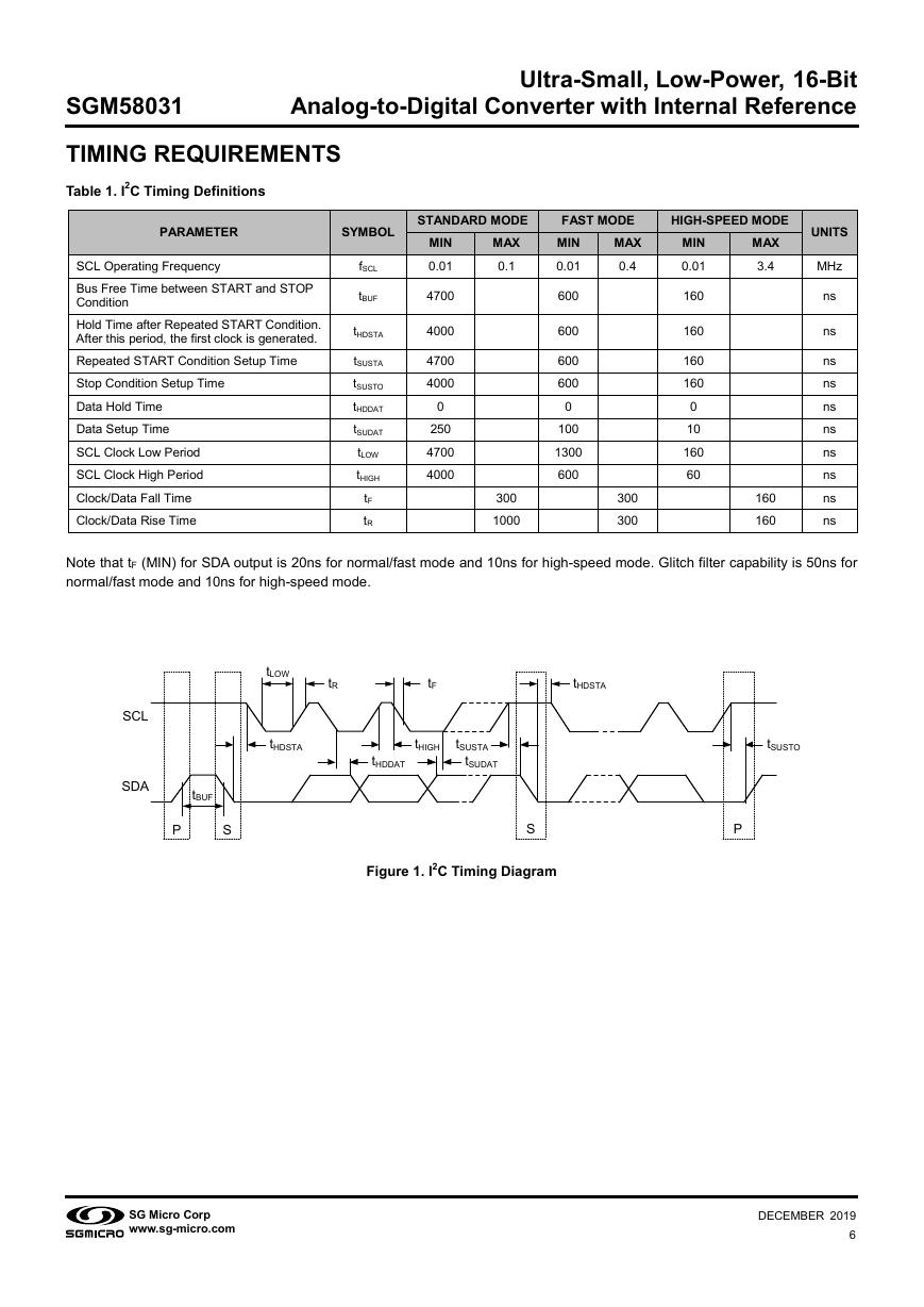
TIMING REQUIREMENTS
Table 1. I2C Timing Definitions
PARAMETER
SYMBOL
SCL Operating Frequency
Bus Free Time between START and STOP
Condition
Hold Time after Repeated START Condition.
After this period, the first clock is generated.
Repeated START Condition Setup Time
Stop Condition Setup Time
Data Hold Time
Data Setup Time
SCL Clock Low Period
SCL Clock High Period
Clock/Data Fall Time
Clock/Data Rise Time
fSCL
tBUF
tHDSTA
tSUSTA
tSUSTO
tHDDAT
tSUDAT
tLOW
tHIGH
tF
tR
STANDARD MODE
MAX
0.1
MIN
0.01
FAST MODE
MAX
MIN
0.01
0.4
4700
4000
4700
4000
0
250
4700
4000
300
1000
600
600
600
600
0
100
1300
600
300
300
HIGH-SPEED MODE
MIN
0.01
160
160
160
160
0
10
160
60
MAX
3.4
160
160
UNITS
MHz
ns
ns
ns
ns
ns
ns
ns
ns
ns
ns
Note that tF (MIN) for SDA output is 20ns for normal/fast mode and 10ns for high-speed mode. Glitch filter capability is 50ns for
normal/fast mode and 10ns for high-speed mode.
tLOW
tR
tF
tHDSTA
SCL
SDA
tBUF
P
S
tHDSTA
tHIGH
tSUSTA
tSUDAT
tHDDAT
S
Figure 1. I2C Timing Diagram
tSUSTO
P
SG Micro Corp
www.sg-micro.com
DECEMBER 2019
6
�
Ultra-Small, Low-Power, 16-Bit
Analog-to-Digital Converter with Internal Reference
SGM58031
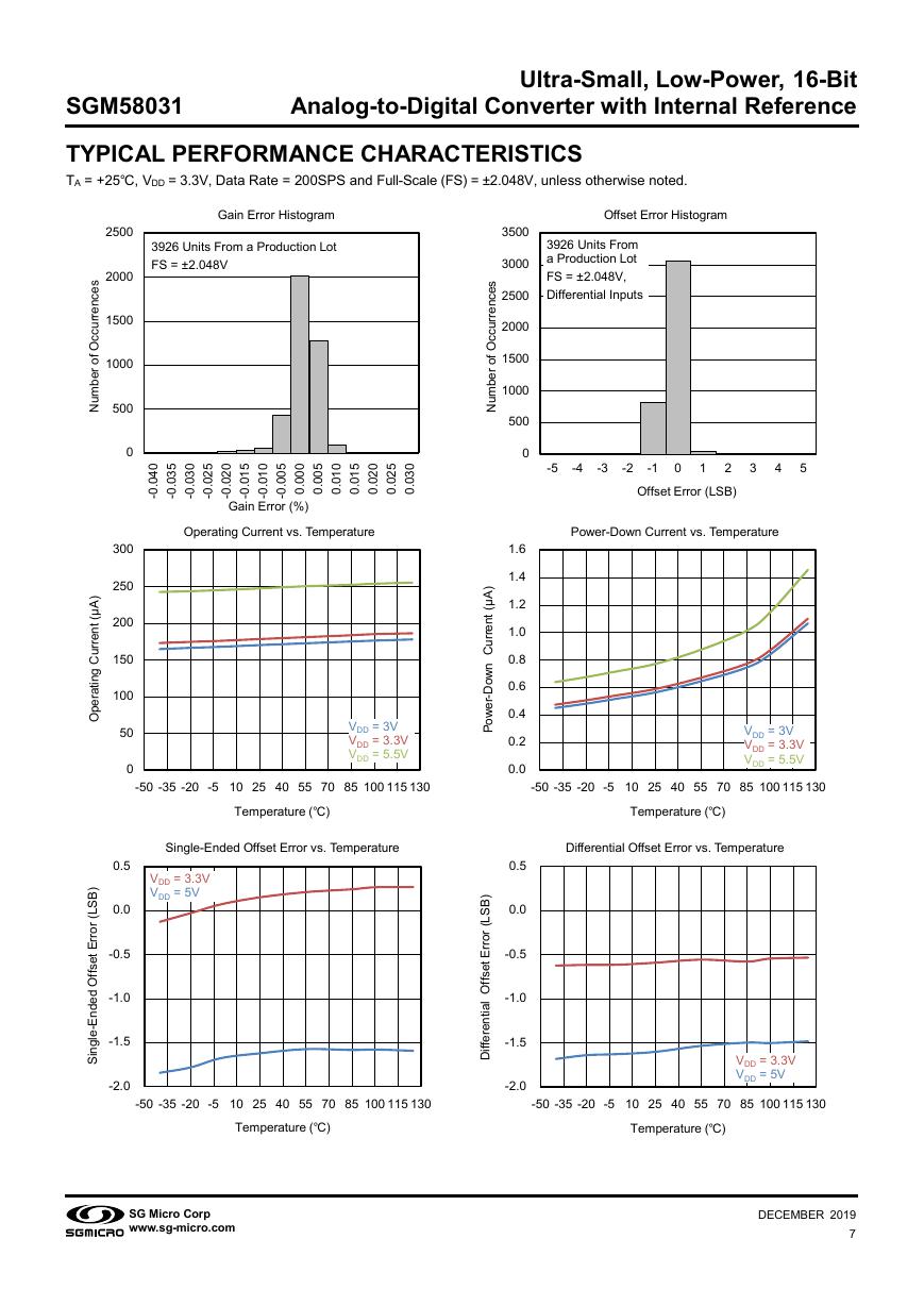
TYPICAL PERFORMANCE CHARACTERISTICS
TA = +25℃, VDD = 3.3V, Data Rate = 200SPS and Full-Scale (FS) = ±2.048V, unless otherwise noted.
Gain Error Histogram
Offset Error Histogram
3030 Samples
3926 Units From a Production Lot
1 Production Lot
FS = ±2.048V
s
e
c
n
e
r
r
u
c
c
O
f
o
r
e
b
m
u
N
2500
2000
1500
1000
500
0
s
e
c
n
e
r
r
u
c
c
O
f
o
r
e
b
m
u
N
3500
3000
2500
2000
1500
1000
500
0
0
4
0
.
0
-
5
3
0
.
0
-
0
3
0
.
0
-
5
2
0
.
0
-
0
2
0
.
0
-
0
0
0
.
0
5
0
0
.
0
0
1
0
.
0
5
1
0
.
0
0
2
0
.
0
5
2
0
.
0
0
3
0
.
0
5
1
0
.
0
-
0
1
0
.
0
-
5
0
0
.
0
-
Gain Error (%)
Operating Current vs. Temperature
VDD = 3V
VDD = 3.3V
VDD = 5.5V
300
250
200
150
100
50
0
)
A
μ
(
t
n
e
r
r
u
C
n
w
o
D
-
r
e
w
o
P
3926 Units From
3030 Samples
a Production Lot
1 Production Lot
FS = ±2.048V,
Differential Inputs
-5
-4
-3
-2
1
0
-1
2
Offset Error (LSB)
3
4
5
Power-Down Current vs. Temperature
VDD = 3V
VDD = 3.3V
VDD = 5.5V
1.6
1.4
1.2
1.0
0.8
0.6
0.4
0.2
0.0
-50 -35 -20 -5 10 25 40 55 70 85 100 115 130
-50 -35 -20 -5 10 25 40 55 70 85 100 115 130
Temperature (℃)
Temperature (℃)
)
A
μ
(
t
n
e
r
r
u
C
g
n
i
t
a
r
e
p
O
)
B
S
L
(
r
o
r
r
E
t
e
s
f
f
O
d
e
d
n
E
-
e
g
n
S
i
l
Single-Ended Offset Error vs. Temperature
VDD = 3.3V
VDD = 5V
0.5
0.0
-0.5
-1.0
-1.5
-2.0
-50 -35 -20 -5 10 25 40 55 70 85 100 115 130
Temperature (℃)
SG Micro Corp
www.sg-micro.com
)
B
S
L
(
r
o
r
r
E
t
e
s
f
f
O
l
a
i
t
n
e
r
e
f
f
i
D
0.5
0.0
-0.5
-1.0
-1.5
-2.0
Differential Offset Error vs. Temperature
VDD = 3.3V
VDD = 5V
-50 -35 -20 -5 10 25 40 55 70 85 100 115 130
Temperature (℃)
DECEMBER 2019
7
�
Ultra-Small, Low-Power, 16-Bit
Analog-to-Digital Converter with Internal Reference
SGM58031
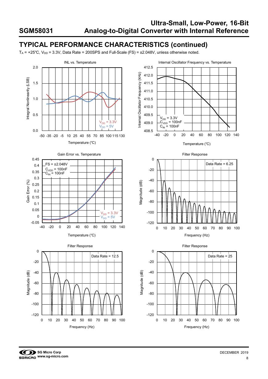
TYPICAL PERFORMANCE CHARACTERISTICS (continued)
TA = +25℃, VDD = 3.3V, Data Rate = 200SPS and Full-Scale (FS) = ±2.048V, unless otherwise noted.
INL vs. Temperature
Internal Oscillator Frequency vs. Temperature
VDD = 3.3V
VDD = 5V
-50 -35 -20 -5 10 25 40 55 70 85 100 115 130
Temperature (℃)
Gain Error vs. Temperature
FS = ±2.048V
CVDD = 100nF
CIN = 100nF
VDD = 3.3V
VDD = 5V
-40 -20
0
20
40
60
80 100 120 140
Temperature (℃)
Filter Response
Data Rate = 12.5
2.0
1.5
1.0
0.5
0.0
0.45
0.4
0.35
0.3
0.25
0.2
0.15
0.1
0.05
0
-0.05
0
-20
-40
-60
-80
-100
-120
412.5
VDD = 3.3V
CVDD = 100nF
CIN = 100nF
-40 -20
0
20
40
60
80 100 120 140
Temperature (℃)
Filter Response
Data Rate = 6.25
0
10 20 30 40 50 60 70 80 90 100
Frequency (Hz)
Filter Response
Data Rate = 25
)
z
H
k
(
y
c
n
e
u
q
e
r
F
r
o
t
a
l
l
i
c
s
O
l
a
n
r
e
t
n
I
412.0
411.5
411.0
410.5
410.0
409.5
409.0
408.5
)
B
d
(
e
d
u
t
i
n
g
a
M
)
B
d
(
e
d
u
t
i
n
g
a
M
0
-20
-40
-60
-80
-100
-120
0
-20
-40
-60
-80
-100
-120
)
B
S
L
(
y
t
i
r
a
e
n
i
l
n
o
N
l
a
r
g
e
t
n
I
)
%
(
r
o
r
r
E
n
a
G
i
)
B
d
(
e
d
u
t
i
n
g
a
M
0
10 20 30 40 50 60 70 80 90 100
0
10 20 30 40 50 60 70 80 90 100
Frequency (Hz)
Frequency (Hz)
SG Micro Corp
www.sg-micro.com
DECEMBER 2019
8
�


 V2版本原理图(Capacitive-Fingerprint-Reader-Schematic_V2).pdf
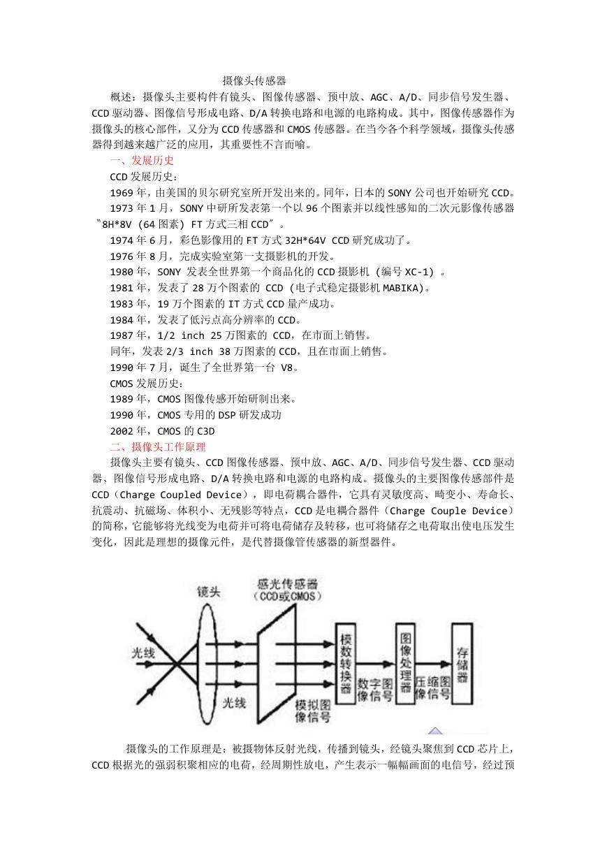 摄像头工作原理.doc
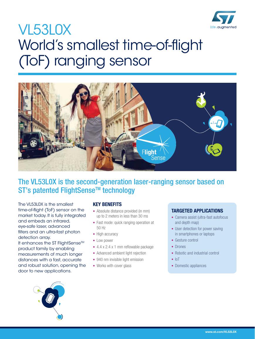 VL53L0X简要说明(En.FLVL53L00216).pdf
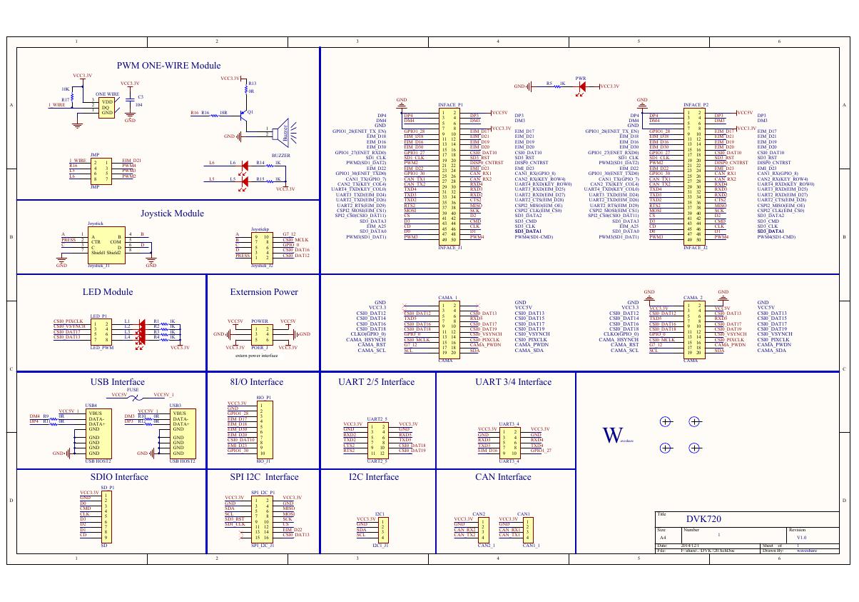 原理图(DVK720-Schematic).pdf
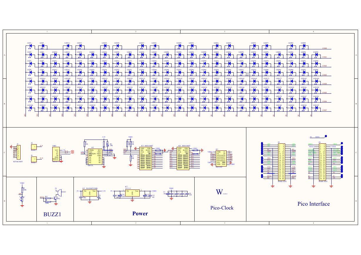 原理图(Pico-Clock-Green-Schdoc).pdf
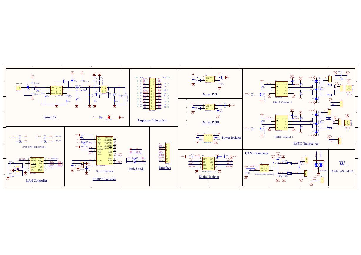 原理图(RS485-CAN-HAT-B-schematic).pdf
 File:SIM7500_SIM7600_SIM7800 Series_SSL_Application Note_V2.00.pdf
 ADS1263(Ads1262).pdf
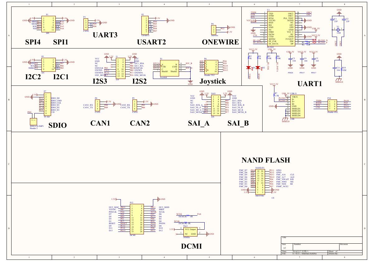 原理图(Open429Z-D-Schematic).pdf
 用户手册(Capacitive_Fingerprint_Reader_User_Manual_CN).pdf
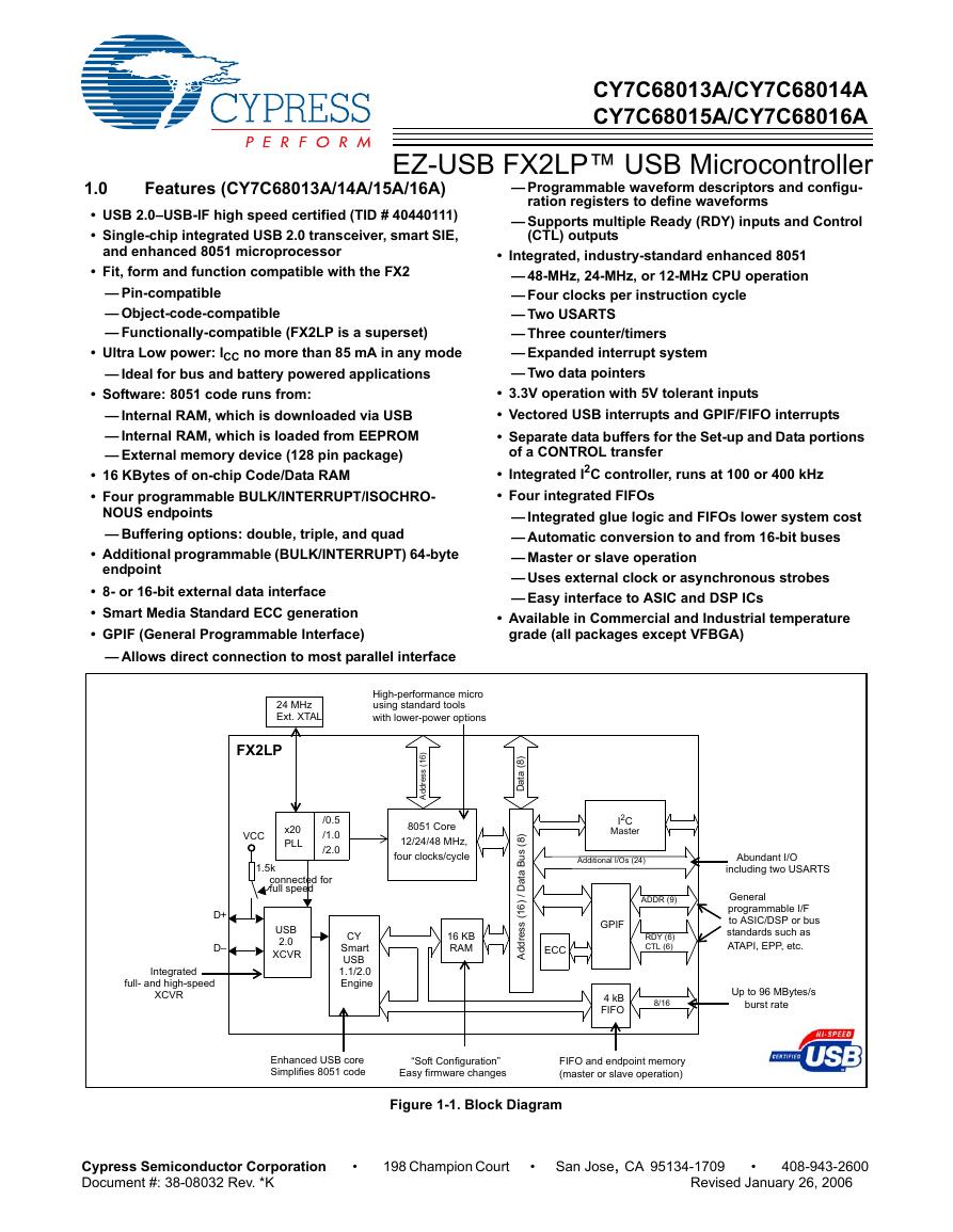 CY7C68013A(英文版)(CY7C68013A).pdf
 TechnicalReference_Dem.pdf