General Description
TCS3472
Color Light-to-Digital Converter with
IR Filter
The TCS3472 device provides a digital return of red, green, blue
(RGB), and clear light sensing values. An IR blocking filter,
integrated on-chip and localized to the color sensing
photodiodes, minimizes the IR spectral component of the
incoming light and allows color measurements to be made
accurately. The high sensitivity, wide dynamic range, and IR
blocking filter make the TCS3472 an ideal color sensor solution
for use under varying lighting conditions and through
attenuating materials.
The TCS3472 color sensor has a wide range of applications
including RGB LED backlight control, solid-state lighting,
health/fitness products, industrial process controls and medical
diagnostic equipment. In addition, the IR blocking filter enables
the TCS3472 to perform ambient light sensing (ALS). Ambient
light sensing is widely used in display-based products such as
cell phones, notebooks, and TVs to sense the lighting
environment and enable automatic display brightness for
optimal viewing and power savings. The TCS3472, itself, can
enter a lower-power wait state between light sensing
measurements to further reduce the average power
consumption.
Ordering Information and Content Guide appear at end of
datasheet.
Key Benefits & Features
The benefits and features of TCS3472, Color Light-to-Digital
Converter with IR Filter are listed below:
Figure 1:
Added Value of Using TCS3472
Benefits
Features
• Enables accurate color and light sensing
measurements under varying lighting
conditions by minimizing IR and UV spectral
component effects
• Red, Green, Blue (RGB), and Clear Light
• Sensing with IR blocking filter
• Programmable analog gain and integration time
• 3,800,000:1 dynamic range
• Very high sensitivity - ideally suited for operation behind
dark glass
• Programmable interrupt pin enables
level-style interrupts when pre-set values are
exceeded, thus reducing companion
micro-processor overhead
• Maskable interrupt
• Programmable upper and lower thresholds with
persistence filter
ams Datasheet
[v1-02] 2016-Feb-08
Page 1
Document Feedback
�
TCS3472 − General Description
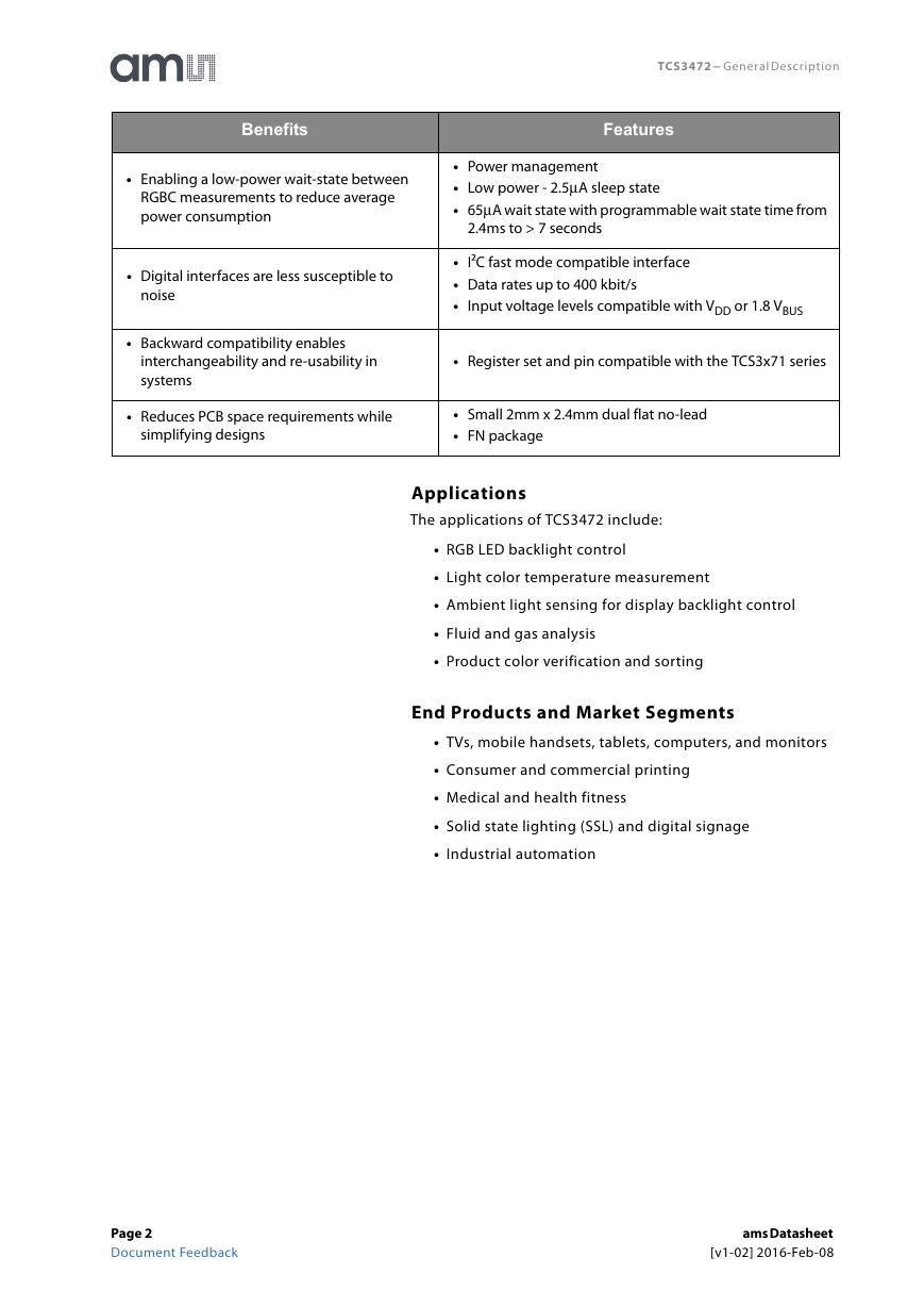
Benefits
Features
• Enabling a low-power wait-state between
RGBC measurements to reduce average
power consumption
• Digital interfaces are less susceptible to
noise
• Backward compatibility enables
interchangeability and re-usability in
systems
• Power management
• Low power - 2.5μA sleep state
• 65μA wait state with programmable wait state time from
2.4ms to > 7 seconds
• I²C fast mode compatible interface
• Data rates up to 400 kbit/s
• Input voltage levels compatible with VDD or 1.8 VBUS
• Register set and pin compatible with the TCS3x71 series
• Reduces PCB space requirements while
simplifying designs
• Small 2mm x 2.4mm dual flat no-lead
• FN package
Applications
The applications of TCS3472 include:
• RGB LED backlight control
• Light color temperature measurement
• Ambient light sensing for display backlight control
• Fluid and gas analysis
• Product color verification and sorting
End Products and Market Segments
• TVs, mobile handsets, tablets, computers, and monitors
• Consumer and commercial printing
• Medical and health fitness
• Solid state lighting (SSL) and digital signage
• Industrial automation
Page 2
Document Feedback
ams Datasheet
[v1-02] 2016-Feb-08
�
TCS3472 − General Description
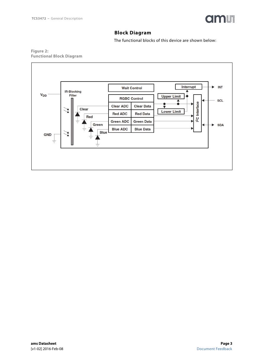
Figure 2:
Functional Block Diagram
Block Diagram
The functional blocks of this device are shown below:
ams Datasheet
[v1-02] 2016-Feb-08
Page 3
Document Feedback
�
Detailed Description
TCS3472 − Detailed Description
The TCS3472 light-to-digital converter contains a 3 × 4
photodiode array, four analog-to-digital converters (ADC) that
integrate the photodiode current, data registers, a state
machine, and an I²C interface. The 3 × 4 photodiode array is
composed of red-filtered, green-filtered, blue-filtered, and
clear (unfiltered) photodiodes. In addition, the photodiodes are
coated with an IR-blocking filter. The four integrating ADCs
simultaneously convert the amplified photodiode currents to a
16-bit digital value. Upon completion of a conversion cycle, the
results are transferred to the data registers, which are
double-buffered to ensure the integrity of the data. All of the
internal timing, as well as the low-power wait state, is controlled
by the state machine.
Communication of the TCS3472 data is accomplished over a
fast, up to 400 kHz, two-wire I²C serial bus. The industry
standard I²C bus facilitates easy, direct connection to
microcontrollers and embedded processors.
In addition to the I²C bus, the TCS3472 provides a separate
interrupt signal output. When interrupts are enabled, and
user-defined thresholds are exceeded, the active-low interrupt
is asserted and remains asserted until it is cleared by the
controller. This interrupt feature simplifies and improves the
efficiency of the system software by eliminating the need to
poll the TCS3472. The user can define the upper and lower
interrupt thresholds and apply an interrupt persistence filter.
The interrupt persistence filter allows the user to define the
number of consecutive out-of-threshold events necessary
before generating an interrupt. The interrupt output is
open-drain, so it can be wire-ORed with other devices.
Page 4
Document Feedback
ams Datasheet
[v1-02] 2016-Feb-08
�
TCS3472 − Pin Assignment
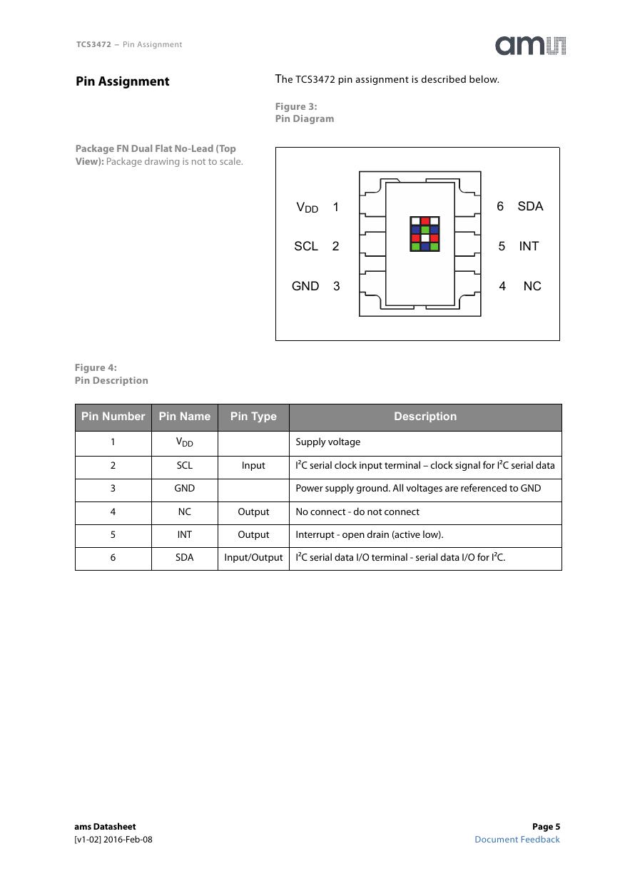
Pin Assignment
Package FN Dual Flat No-Lead (Top
View): Package drawing is not to scale.
The TCS3472 pin assignment is described below.
Figure 3:
Pin Diagram
VDD 1
SCL 2
GND 3
6 SDA
5 INT
4 NC
Figure 4:
Pin Description
Pin Number Pin Name
Pin Type
Description
1
2
3
4
5
6
VDD
SCL
GND
NC
INT
SDA
Supply voltage
Input
I²C serial clock input terminal – clock signal for I²C serial data
Power supply ground. All voltages are referenced to GND
Output
Output
No connect - do not connect
Interrupt - open drain (active low).
Input/Output
I²C serial data I/O terminal - serial data I/O for I²C.
ams Datasheet
[v1-02] 2016-Feb-08
Page 5
Document Feedback
�
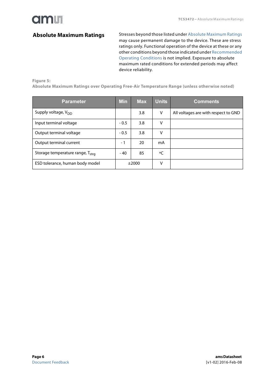
Absolute Maximum Ratings
TCS3472 − Absolute Maximum Ratings
Stresses beyond those listed under Absolute Maximum Ratings
may cause permanent damage to the device. These are stress
ratings only. Functional operation of the device at these or any
other conditions beyond those indicated under Recommended
Operating Conditions is not implied. Exposure to absolute
maximum rated conditions for extended periods may affect
device reliability.
Figure 5:
Absolute Maximum Ratings over Operating Free-Air Temperature Range (unless otherwise noted)
Parameter
Min
Max
Units
Comments
All voltages are with respect to GND
Supply voltage, VDD
Input terminal voltage
Output terminal voltage
Output terminal current
Storage temperature range, Tstrg
3.8
3.8
3.8
20
85
- 0.5
- 0.5
- 1
- 40
ESD tolerance, human body model
±2000
V
V
V
mA
ºC
V
Page 6
Document Feedback
ams Datasheet
[v1-02] 2016-Feb-08
�
TCS3472 − Electrical Characteristics
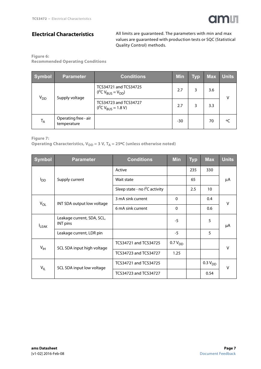
Electrical Characteristics
Figure 6:
Recommended Operating Conditions
All limits are guaranteed. The parameters with min and max
values are guaranteed with production tests or SQC (Statistical
Quality Control) methods.
Symbol
Parameter
Conditions
Min
Typ Max Units
TCS34721 and TCS34725
(I²C VBUS = VDD)
TCS34723 and TCS34727
(I²C VBUS = 1.8 V)
VDD
Supply voltage
TA
Operating free - air
temperature
3
3
2.7
2.7
-30
3.6
3.3
70
V
ºC
Figure 7:
Operating Characteristics, VDD = 3 V, TA = 25ºC (unless otherwise noted)
Symbol
Parameter
Conditions
Min
Typ Max
Units
IDD
Supply current
VOL
INT SDA output low voltage
Active
Wait state
Sleep state - no I²C activity
3 mA sink current
6 mA sink current
235
65
2.5
330
10
0.4
0.6
5
5
0
0
-5
-5
μA
V
μA
V
V
Leakage current, SDA, SCL,
INT pins
Leakage current, LDR pin
SCL SDA input high voltage
ILEAK
VIH
VIL
TCS34721 and TCS34725
0.7 VDD
TCS34723 and TCS34727
1.25
SCL SDA input low voltage
TCS34721 and TCS34725
TCS34723 and TCS34727
0.3 VDD
0.54
ams Datasheet
[v1-02] 2016-Feb-08
Page 7
Document Feedback
�
TCS3472 − Electrical Characteristics
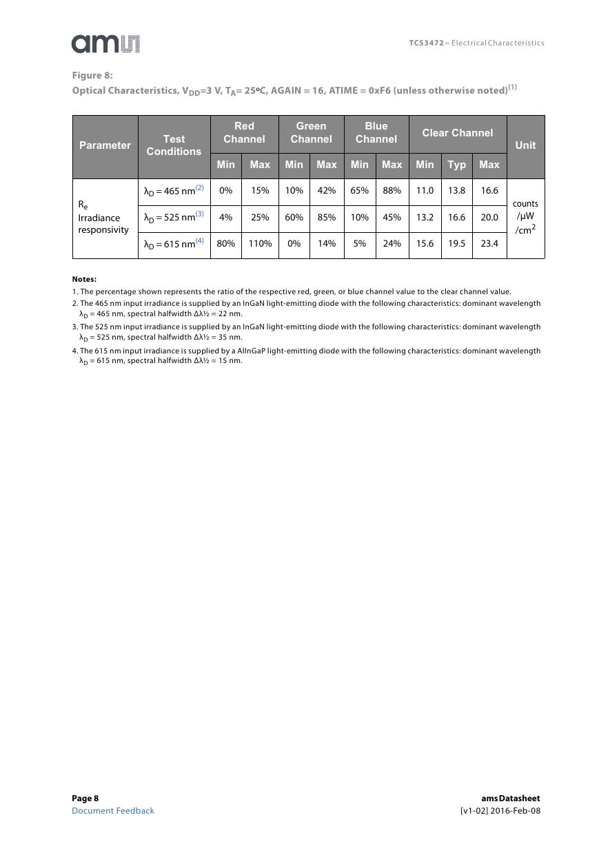
Figure 8:
Optical Characteristics, VDD=3 V, TA= 25ºC, AGAIN = 16, ATIME = 0xF6 (unless otherwise noted)(1)
Parameter
Test
Conditions
Re
Irradiance
responsivity
λD = 465 nm(2)
λD = 525 nm(3)
λD = 615 nm(4)
Red
Channel
Green
Channel
Blue
Channel
Clear Channel
Min Max Min Max Min Max Min
Typ Max
0%
15%
10%
42%
65%
88%
11.0
13.8
16.6
4%
25%
60%
85%
10%
45%
13.2
16.6
20.0
80%
110%
0%
14%
5%
24%
15.6
19.5
23.4
Unit
counts
/μW
/cm2
Notes:
1. The percentage shown represents the ratio of the respective red, green, or blue channel value to the clear channel value.
2. The 465 nm input irradiance is supplied by an InGaN light-emitting diode with the following characteristics: dominant wavelength
λD = 465 nm, spectral halfwidth Δλ½ = 22 nm.
3. The 525 nm input irradiance is supplied by an InGaN light-emitting diode with the following characteristics: dominant wavelength
λD = 525 nm, spectral halfwidth Δλ½ = 35 nm.
4. The 615 nm input irradiance is supplied by a AlInGaP light-emitting diode with the following characteristics: dominant wavelength
λD = 615 nm, spectral halfwidth Δλ½ = 15 nm.
Page 8
Document Feedback
ams Datasheet
[v1-02] 2016-Feb-08
�



 V2版本原理图(Capacitive-Fingerprint-Reader-Schematic_V2).pdf
 摄像头工作原理.doc
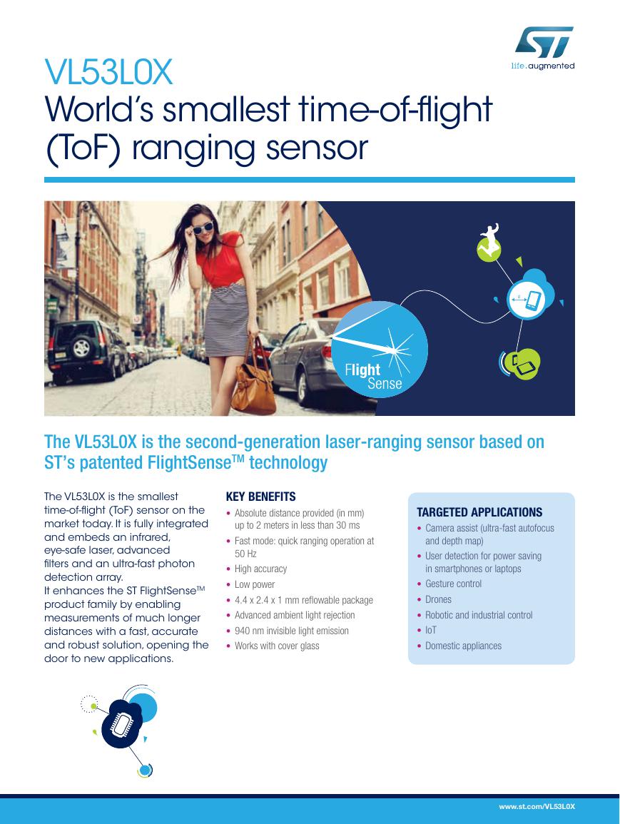 VL53L0X简要说明(En.FLVL53L00216).pdf
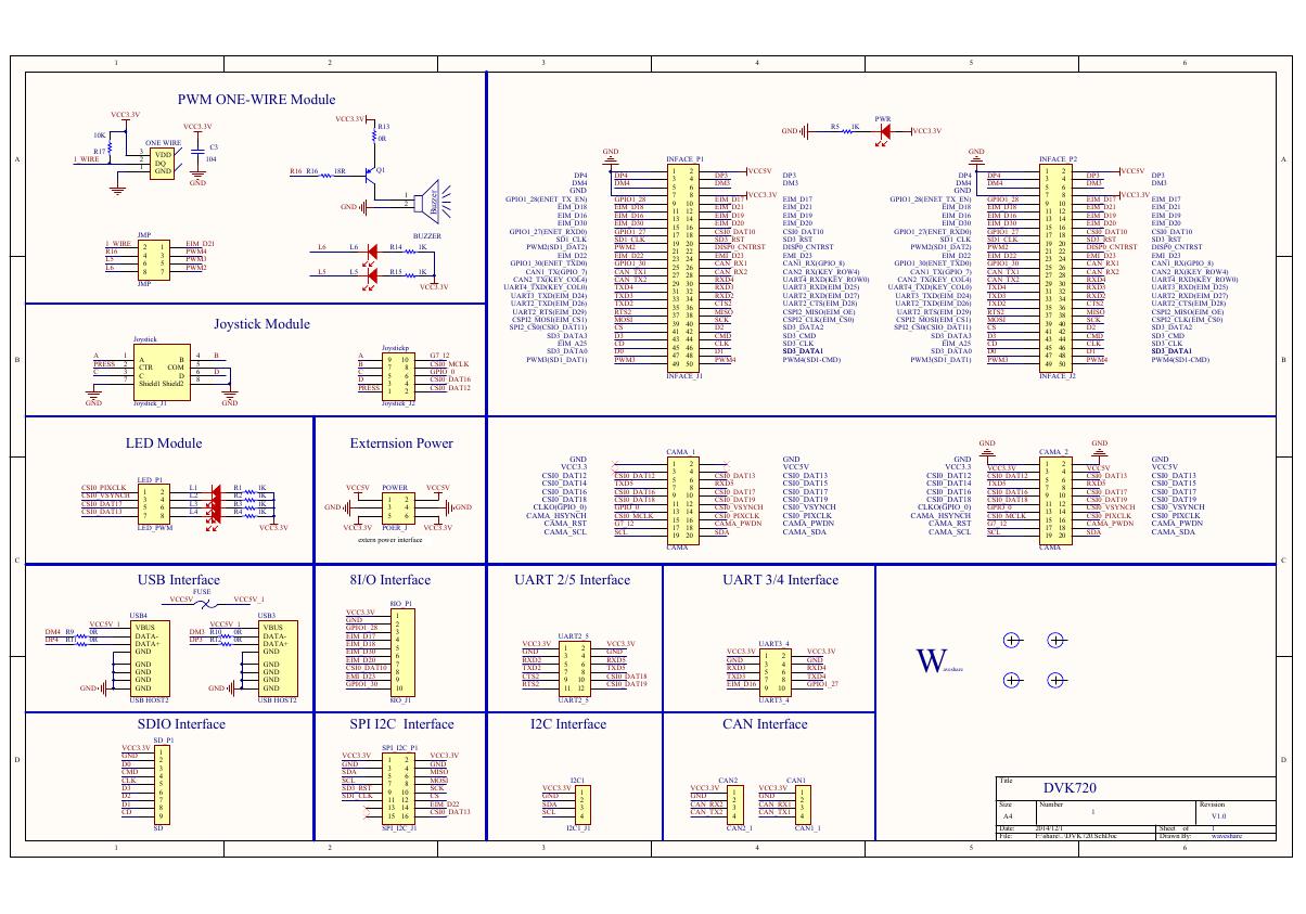 原理图(DVK720-Schematic).pdf
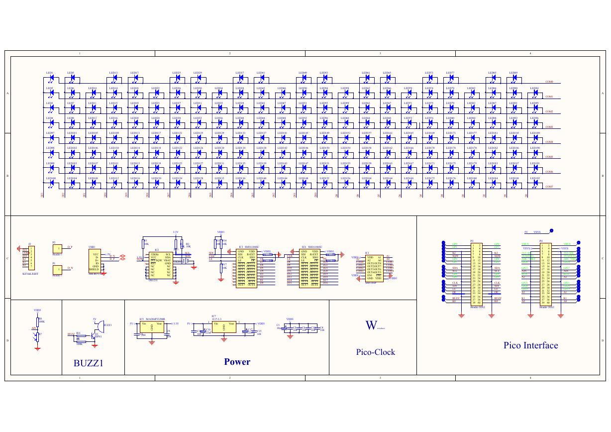 原理图(Pico-Clock-Green-Schdoc).pdf
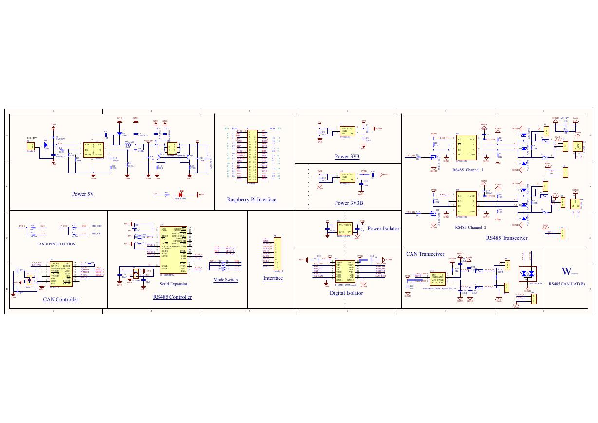 原理图(RS485-CAN-HAT-B-schematic).pdf
 File:SIM7500_SIM7600_SIM7800 Series_SSL_Application Note_V2.00.pdf
 ADS1263(Ads1262).pdf
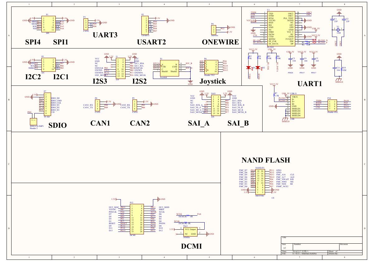 原理图(Open429Z-D-Schematic).pdf
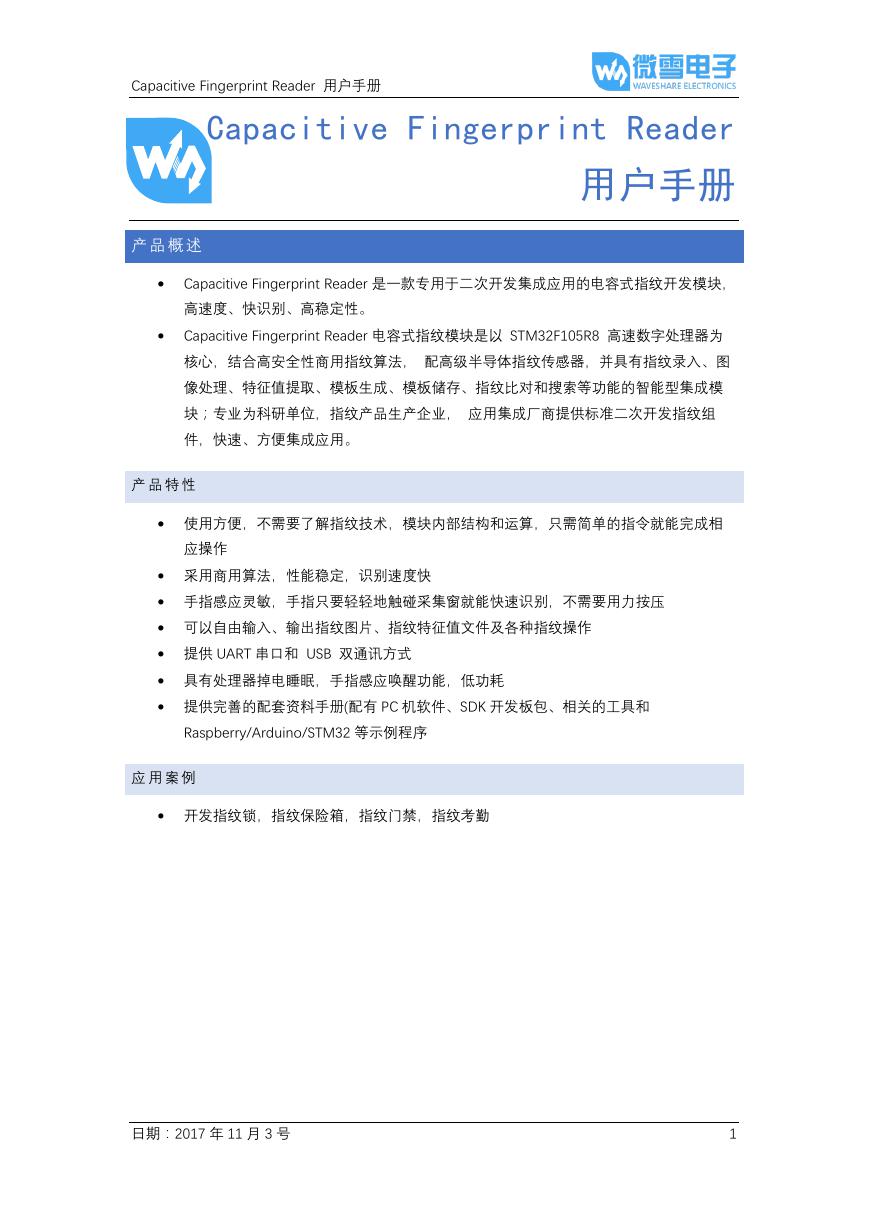 用户手册(Capacitive_Fingerprint_Reader_User_Manual_CN).pdf
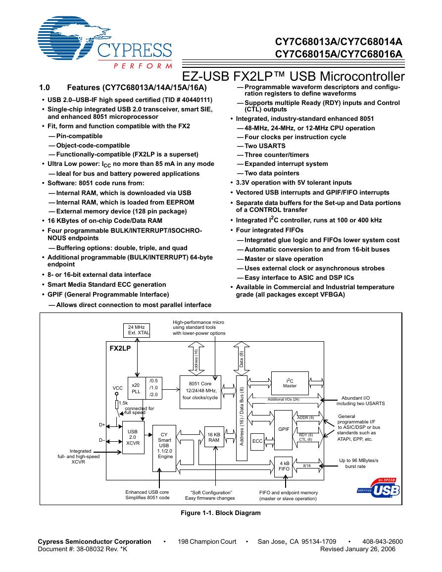 CY7C68013A(英文版)(CY7C68013A).pdf
 TechnicalReference_Dem.pdf