ADS101x Ultra-Small, Low-Power, I2C-Compatible, 3.3-kSPS, 12-Bit ADCs
With Internal Reference, Oscillator, and Programmable Comparator
ADS1013, ADS1014, ADS1015
SBAS473E –MAY 2009–REVISED JANUARY 2018
1 Features
1• Ultra-Small X2QFN Package:
2 mm × 1.5 mm × 0.4 mm
12-Bit Noise-Free Resolution
•
• Wide Supply Range: 2.0 V to 5.5 V
Low Current Consumption: 150 μA
•
(Continuous-Conversion Mode)
• Programmable Data Rate:
128 SPS to 3.3 kSPS
• Single-Cycle Settling
Internal Low-Drift Voltage Reference
•
Internal Oscillator
•
I2C Interface: Four Pin-Selectable Addresses
•
• Four Single-Ended or Two Differential Inputs
(ADS1015)
• Programmable Comparator (ADS1014 and
ADS1015)
• Operating Temperature Range:
–40°C to +125°C
2 Applications
• Portable Instrumentation
• Battery Voltage and Current Monitoring
• Temperature Measurement Systems
• Consumer Electronics
• Factory Automation and Process Control
low-power, 12-bit,
3 Description
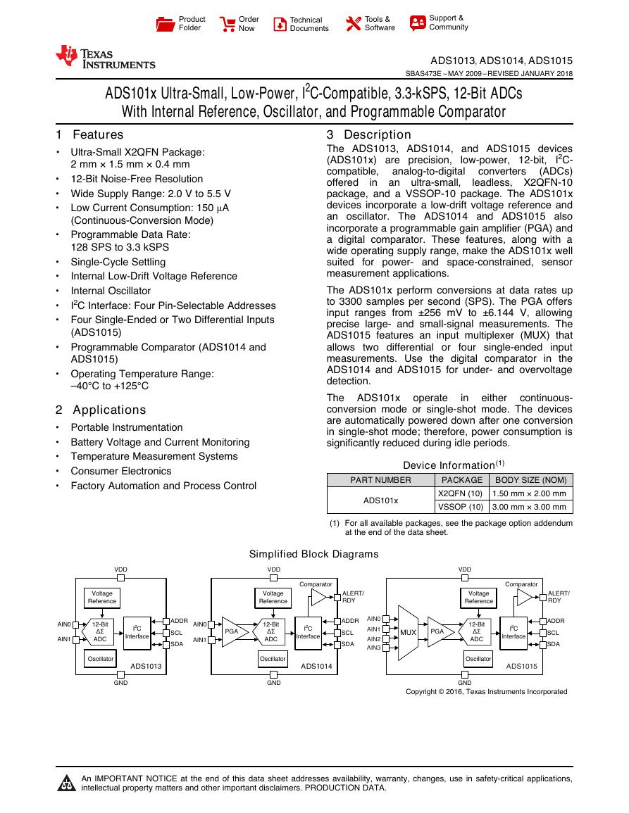
The ADS1013, ADS1014, and ADS1015 devices
I2C-
(ADS101x) are precision,
converters
compatible,
analog-to-digital
(ADCs)
offered in an ultra-small,
leadless, X2QFN-10
package, and a VSSOP-10 package. The ADS101x
devices incorporate a low-drift voltage reference and
an oscillator. The ADS1014 and ADS1015 also
incorporate a programmable gain amplifier (PGA) and
a digital comparator. These features, along with a
wide operating supply range, make the ADS101x well
suited for power- and space-constrained, sensor
measurement applications.
The ADS101x perform conversions at data rates up
to 3300 samples per second (SPS). The PGA offers
input ranges from ±256 mV to ±6.144 V, allowing
precise large- and small-signal measurements. The
ADS1015 features an input multiplexer (MUX) that
four single-ended input
allows two differential or
measurements. Use the digital comparator
in the
ADS1014 and ADS1015 for under- and overvoltage
detection.
The ADS101x
continuous-
conversion mode or single-shot mode. The devices
are automatically powered down after one conversion
in single-shot mode; therefore, power consumption is
significantly reduced during idle periods.
operate
in
either
Device Information(1)
PART NUMBER
ADS101x
BODY SIZE (NOM)
PACKAGE
1.50 mm × 2.00 mm
X2QFN (10)
VSSOP (10) 3.00 mm × 3.00 mm
(1) For all available packages, see the package option addendum
at the end of the data sheet.
Simplified Block Diagrams
1
An IMPORTANT NOTICE at the end of this data sheet addresses availability, warranty, changes, use in safety-critical applications,
intellectual property matters and other important disclaimers. PRODUCTION DATA.
VoltageReferenceOscillatorSCLSDAADDRADS1013AIN1GNDAIN0VDDI2CInterface12-Bit ßflADCADS1014OscillatorComparatorALERT/RDYPGAADS1015AIN0AIN1AIN2AIN3Copyright © 2016, Texas Instruments IncorporatedAIN1AIN0MUXSCLSDAADDRI2CInterface12-Bit ßflADCVoltageReferenceOscillatorComparatorALERT/RDYPGASCLSDAADDRI2CInterface12-Bit ßflADCVoltageReferenceGNDVDDGNDVDDProductFolderOrderNowTechnicalDocumentsTools &SoftwareSupport &Community�
ADS1013, ADS1014, ADS1015
SBAS473E –MAY 2009–REVISED JANUARY 2018
www.ti.com
Table of Contents
1
Features.................................................................. 1
2 Applications ........................................................... 1
3 Description ............................................................. 1
4 Revision History..................................................... 2
5 Device Comparison Table..................................... 4
6 Pin Configuration and Functions ......................... 4
7 Specifications......................................................... 5
7.1 Absolute Maximum Ratings ...................................... 5
7.2 ESD Ratings.............................................................. 5
7.3 Recommended Operating Conditions....................... 5
7.4 Thermal Information.................................................. 5
7.5 Electrical Characteristics.......................................... 6
7.6 Timing Requirements: I2C......................................... 7
7.7 Typical Characteristics.............................................. 8
8 Detailed Description .............................................. 9
8.1 Overview ................................................................... 9
8.2 Functional Block Diagrams ....................................... 9
8.3 Feature Description................................................. 10
8.4 Device Functional Modes........................................ 16
8.5 Programming........................................................... 17
8.6 Register Map........................................................... 22
9 Application and Implementation ........................ 26
9.1 Application Information............................................ 26
9.2 Typical Application ................................................. 31
10 Power Supply Recommendations ..................... 35
10.1 Power-Supply Sequencing.................................... 35
10.2 Power-Supply Decoupling..................................... 35
11 Layout................................................................... 36
11.1 Layout Guidelines ................................................. 36
11.2 Layout Example .................................................... 37
12 Device and Documentation Support ................. 38
12.1 Documentation Support ........................................ 38
12.2 Related Links ........................................................ 38
12.3 Receiving Notification of Documentation Updates 38
12.4 Community Resources.......................................... 38
12.5 Trademarks ........................................................... 38
12.6 Electrostatic Discharge Caution............................ 38
12.7 Glossary ................................................................ 38
13 Mechanical, Packaging, and Orderable
Information ........................................................... 39
4 Revision History
NOTE: Page numbers for previous revisions may differ from page numbers in the current version.
Changes from Revision D (December 2016) to Revision E
Page
• Changed Digital input voltage max value from VDD + 0.3 V to 5.5 V in Absolute Maximum Ratings table.......................... 5
• Changed VDIG max value from VDD to 5.5 V in Recommended Operating Conditions table ............................................... 5
• Added "over temperature" to Offset drift parameter for clarity ............................................................................................... 6
• Added Long-term offset drift parameter in Electrical Characteristics table ............................................................................ 6
• Added "over temperature" to Gain drift parameter for clarity ................................................................................................. 6
• Added Long-term gain drift parameter in Electrical Characteristics table .............................................................................. 6
• Changed VIH parameter max value from VDD to 5.5 V in Electrical Characteristics table .................................................... 6
• Added Output Data Rate and Conversion Time section for clarity....................................................................................... 12
• Changed Figure 13, ALERT Pin Timing Diagram for clarity................................................................................................. 14
• Changed Figure 24, Typical Connections of the ADS1015 for clarity.................................................................................. 26
• Changed resistor values in Figure 28, Basic Hardware Configuration, from 10 Ω to 10 kΩ ............................................... 30
Changes from Revision C (October 2009) to Revision D
Page
• Added Device Information, ESD Ratings, Recommended Operating Conditions, and Thermal Information tables,
and Parameter Measurement Information, Detailed Description, Application and Implementation, Power Supply
Recommendations, Layout, Device and Documentation Support, and sections.................................................................... 1
• Changed Title, and Description, Features, and Applications sections for clarity ................................................................... 1
• Deleted temperature range text from Description section and moved to Features section ................................................... 1
• Changed Product Family table title to Device Comparison Table and deleted Package Designator column........................ 4
• Changed Pin Functions table for clarity.................................................................................................................................. 4
• Changed Power-supply voltage max value from 5.5 V to 7 V in Absolute Maximum Ratings table...................................... 5
• Changed Analog input voltage from –0.3 V to GND – 0.3 V in Absolute Maximum Ratings table ........................................ 5
• Changed Digital input voltage min value from –0.5 V to GND – 0.3 V in Absolute Maximum Ratings table......................... 5
2
Submit Documentation Feedback
Copyright © 2009–2018, Texas Instruments Incorporated
Product Folder Links: ADS1013 ADS1014 ADS1015
�
www.ti.com
ADS1013, ADS1014, ADS1015
SBAS473E –MAY 2009–REVISED JANUARY 2018
• Changed Digital input voltage max value from 5.5 V to VDD + 0.3 V in Absolute Maximum Ratings table.......................... 5
• Deleted Analog input current rows in Absolute Maximum Ratings table................................................................................ 5
• Added Input current row in Absolute Maximum Ratings table ............................................................................................... 5
• Added Operating temperature range of –40°C to +125°C back into Absolute Maximum Ratings table................................ 5
• Added minimum specification of –40°C for TJ in Absolute Maximum Ratings table ............................................................. 5
• Changed Electrical Characteristics table conditions line for clarity ........................................................................................ 6
• Changed all instances of "FS" to "FSR" ................................................................................................................................. 6
• Deleted FSR from Electrical Characteristics and moved to Recommended Operating Conditions table .............................. 6
• Added values from Table 2 to Differential input impedance parameter in Electrical Characteristics..................................... 6
• Deleted Output noise parameter from Electrical Characteristics ........................................................................................... 6
• Changed Offset error empty min value to –0.5, and max value from ±0.5 to 0.5 for clarity in Electrical Characteristics
table ........................................................................................................................................................................................ 6
• Changed VIH parameter max value from 5.5 V to VDD in Electrical Characteristics table .................................................... 6
• Changed VIL parameter min value from GND – 0.5 V to GND in Electrical Characteristics table ......................................... 6
• Changed Input leakage current parameters from two rows to one row, changed test conditions from VIH = 5.5V and
VIL = GND to GND < VDIG < VDD, and changed min value from 10 µA to –10 µA in Electrical Characteristics table........... 6
• Deleted Power-supply voltage parameter from Electrical Characteristics and moved to Recommended Operating
Conditions table...................................................................................................................................................................... 6
• Deleted Specified temperature parameter from Electrical Characteristics and moved to Recommended Operating
Conditions table...................................................................................................................................................................... 6
• Deleted Storage temperature parameter from Electrical Characteristics to Absolute Maximum Ratings table ..................... 6
• Deleted Operating temperature parameter from Temperature section of Electrical Characteristics table............................. 6
• Changed text in note 1 of Electrical Characteristics table from "In no event should more than VDD + 0.3 V be
applied to this device" to "No more than VDD + 0.3 V must be applied to the analog inputs of the device. See Table
1 for more information." .......................................................................................................................................................... 6
• Added condition statement in Timing Requirements: I2C....................................................................................................... 7
• Added note 1 to Timing Requirements table.......................................................................................................................... 7
• Deleted Figure 7, Noise Plot................................................................................................................................................... 8
• Changed Figure 8; deleted "Gain = 2/3, 1, 2, 4, 8, or 16" from figure .................................................................................. 9
• Added Functional Block Diagrams for ADS1014 and ADS1013 ............................................................................................ 9
• Changed Analog Inputs section to provide LSB size information instead of PGA setting ................................................... 11
• Changed Full-Scale Input section title to Full-Scale Range (FSR) and LSB Size, and updated section for clarity ............. 12
• Added Voltage Reference and Oscillator sections ............................................................................................................... 12
• Changed Comparator section title to Digital Comparator, and updated section for clarity. ................................................. 12
• Changed Conversion Ready Pin section for clarity .............................................................................................................. 14
• Changed Register Map section for clarity ............................................................................................................................ 22
• Changed Application Information section for clarity ............................................................................................................. 26
• Added Input Protection section............................................................................................................................................. 27
• Added Unused Inputs and Outputs section.......................................................................................................................... 27
• Changed Aliasing section title to Analog Input Filtering and updated section for clarity...................................................... 28
• Added Typical Application section........................................................................................................................................ 31
Changes from Revision B (September 2009) to Revision C
Page
• Deleted operating temperature bullet from Features section ................................................................................................. 1
• Deleted Operating temperature range parameter from Absolute Maximum Ratings table .................................................... 5
• Deleted Operating temperature parameter from Temperature subsection of Electrical Characteristics table....................... 6
• Changed Figure 2 to reflect maximum operating temperature............................................................................................... 8
Copyright © 2009–2018, Texas Instruments Incorporated
Submit Documentation Feedback
3
Product Folder Links: ADS1013 ADS1014 ADS1015
�
ADS1013, ADS1014, ADS1015
SBAS473E –MAY 2009–REVISED JANUARY 2018
www.ti.com
• Changed Figure 3 to reflect maximum operating temperature............................................................................................... 8
• Changed Figure 4 to reflect maximum operating temperature............................................................................................... 8
• Changed Figure 5 to reflect maximum operating temperature............................................................................................... 8
• Changed Figure 6 to reflect maximum operating temperature............................................................................................... 8
4
Submit Documentation Feedback
Copyright © 2009–2018, Texas Instruments Incorporated
Product Folder Links: ADS1013 ADS1014 ADS1015
�
www.ti.com
5 Device Comparison Table
DEVICE
ADS1015
ADS1014
ADS1013
ADS1115
ADS1114
ADS1113
ADS1018
ADS1118
RESOLUTION
(Bits)
12
12
12
16
16
16
12
16
MAXIMUM SAMPLE
RATE
(SPS)
3300
3300
3300
860
860
860
3300
860
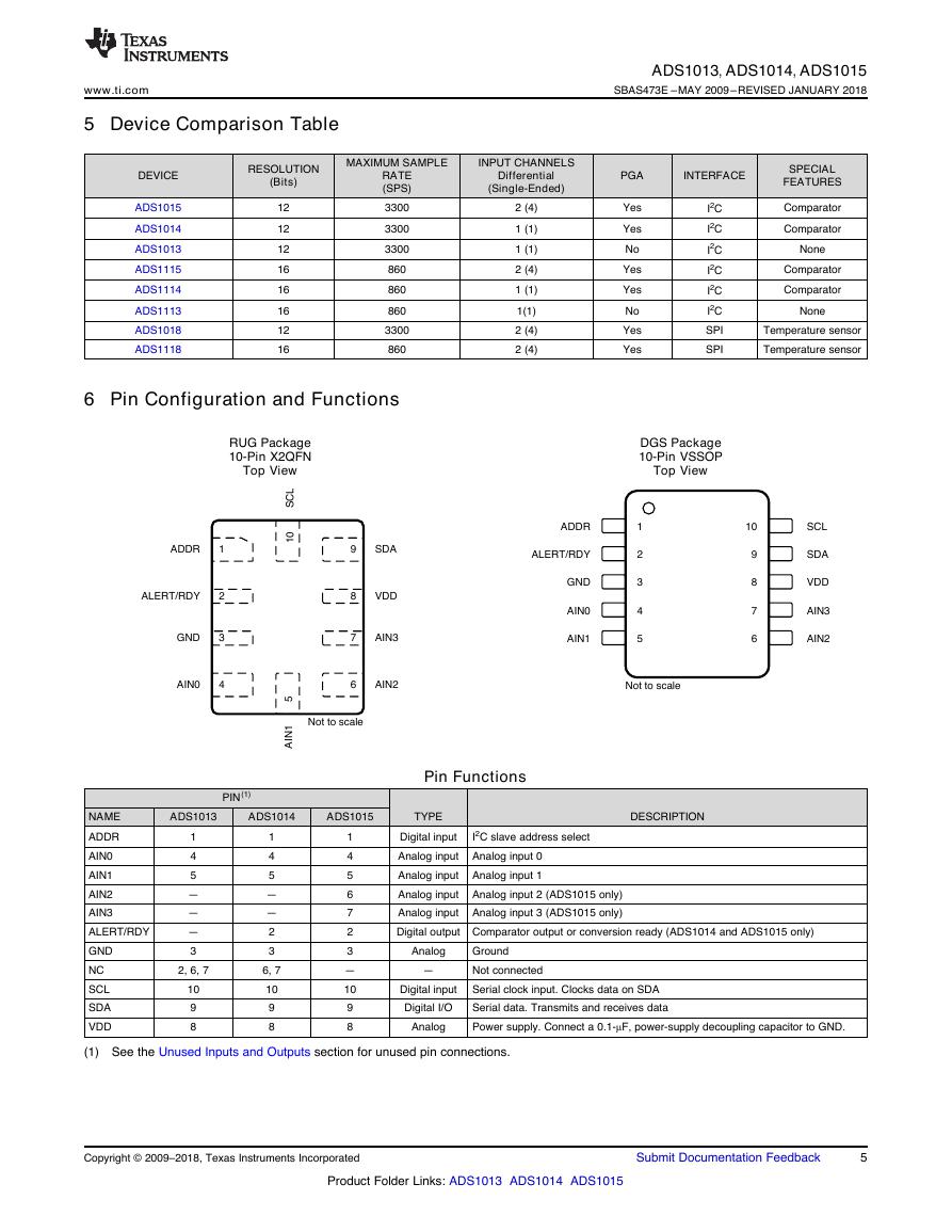
6 Pin Configuration and Functions
ADS1013, ADS1014, ADS1015
SBAS473E –MAY 2009–REVISED JANUARY 2018
PGA
INTERFACE
Yes
Yes
No
Yes
Yes
No
Yes
Yes
I2C
I2C
I2C
I2C
I2C
I2C
SPI
SPI
SPECIAL
FEATURES
Comparator
Comparator
None
Comparator
Comparator
None
Temperature sensor
Temperature sensor
INPUT CHANNELS
Differential
(Single-Ended)
2 (4)
1 (1)
1 (1)
2 (4)
1 (1)
1(1)
2 (4)
2 (4)
RUG Package
10-Pin X2QFN
Top View
DGS Package
10-Pin VSSOP
Top View
PIN(1)
Pin Functions
ADS1013
ADS1014
ADS1015
TYPE
DESCRIPTION
1
4
5
—
—
—
3
2, 6, 7
10
9
8
1
4
5
—
—
2
3
6, 7
10
9
8
1
4
5
6
7
2
3
—
10
9
8
I2C slave address select
Digital input
Analog input Analog input 0
Analog input Analog input 1
Analog input Analog input 2 (ADS1015 only)
Analog input Analog input 3 (ADS1015 only)
Digital output Comparator output or conversion ready (ADS1014 and ADS1015 only)
Analog
—
Digital input
Digital I/O
Analog
Ground
Not connected
Serial clock input. Clocks data on SDA
Serial data. Transmits and receives data
Power supply. Connect a 0.1-μF, power-supply decoupling capacitor to GND.
NAME
ADDR
AIN0
AIN1
AIN2
AIN3
ALERT/RDY
GND
NC
SCL
SDA
VDD
(1) See the Unused Inputs and Outputs section for unused pin connections.
Copyright © 2009–2018, Texas Instruments Incorporated
Submit Documentation Feedback
5
Product Folder Links: ADS1013 ADS1014 ADS1015
1ADDR2ALERT/RDY3GND4AIN05AIN16AIN27AIN38VDD9SDA10SCLNot to scale1ADDR10 SCL2ALERT/RDY9 SDA3GND8 VDD4AIN07 AIN35AIN16 AIN2Not to scale�
ADS1013, ADS1014, ADS1015
SBAS473E –MAY 2009–REVISED JANUARY 2018
7 Specifications
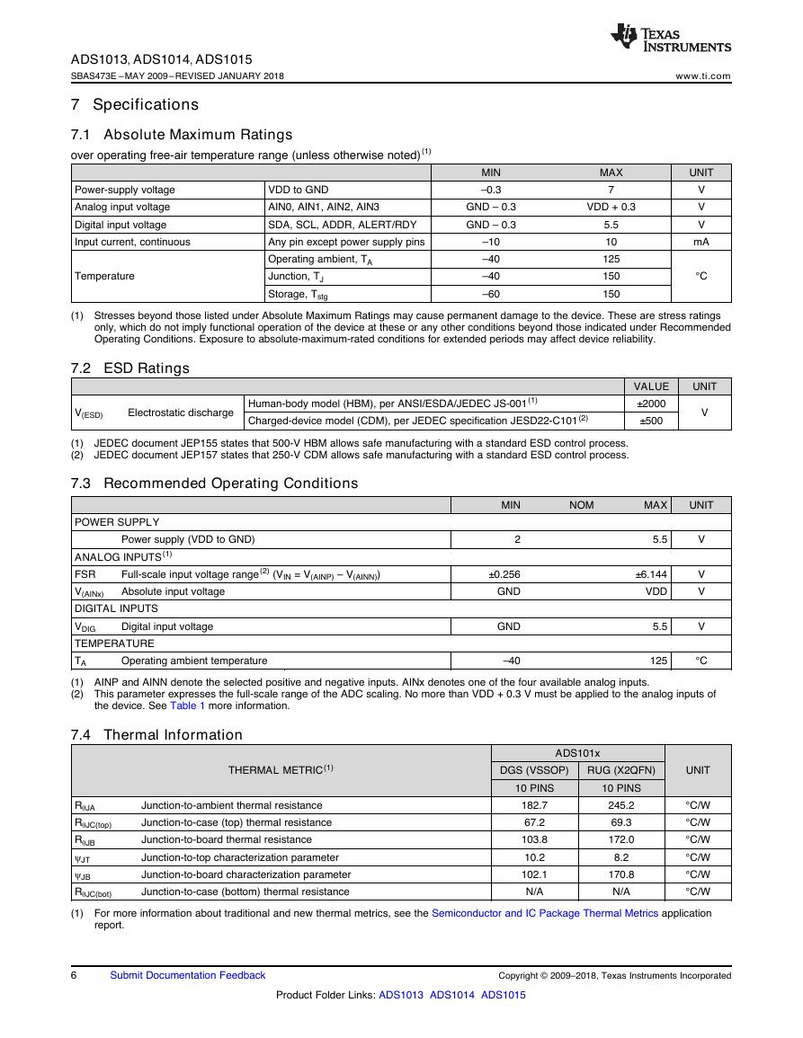
7.1 Absolute Maximum Ratings
over operating free-air temperature range (unless otherwise noted)(1)
www.ti.com
Power-supply voltage
Analog input voltage
Digital input voltage
Input current, continuous
Temperature
VDD to GND
AIN0, AIN1, AIN2, AIN3
SDA, SCL, ADDR, ALERT/RDY
Any pin except power supply pins
Operating ambient, TA
Junction, TJ
Storage, Tstg
MIN
–0.3
GND – 0.3
GND – 0.3
–10
–40
–40
–60
MAX
7
VDD + 0.3
5.5
10
125
150
150
UNIT
V
V
V
mA
°C
(1) Stresses beyond those listed under Absolute Maximum Ratings may cause permanent damage to the device. These are stress ratings
only, which do not imply functional operation of the device at these or any other conditions beyond those indicated under Recommended
Operating Conditions. Exposure to absolute-maximum-rated conditions for extended periods may affect device reliability.
7.2 ESD Ratings
V(ESD)
Electrostatic discharge
Human-body model (HBM), per ANSI/ESDA/JEDEC JS-001(1)
Charged-device model (CDM), per JEDEC specification JESD22-C101(2)
(1)
(2)
JEDEC document JEP155 states that 500-V HBM allows safe manufacturing with a standard ESD control process.
JEDEC document JEP157 states that 250-V CDM allows safe manufacturing with a standard ESD control process.
VALUE
±2000
±500
UNIT
V
7.3 Recommended Operating Conditions
POWER SUPPLY
Power supply (VDD to GND)
MIN
2
NOM
MAX
UNIT
5.5
V
Full-scale input voltage range(2) (VIN = V(AINP) – V(AINN))
Absolute input voltage
ANALOG INPUTS(1)
FSR
V(AINx)
DIGITAL INPUTS
VDIG
TEMPERATURE
TA
(1) AINP and AINN denote the selected positive and negative inputs. AINx denotes one of the four available analog inputs.
(2) This parameter expresses the full-scale range of the ADC scaling. No more than VDD + 0.3 V must be applied to the analog inputs of
Operating ambient temperature
Digital input voltage
±6.144
VDD
±0.256
GND
GND
–40
V
V
V
5.5
125
°C
the device. See Table 1 more information.
7.4 Thermal Information
THERMAL METRIC(1)
DGS (VSSOP)
RUG (X2QFN)
UNIT
ADS101x
RθJA
RθJC(top)
RθJB
ψJT
ψJB
RθJC(bot)
(1) For more information about traditional and new thermal metrics, see the Semiconductor and IC Package Thermal Metrics application
Junction-to-ambient thermal resistance
Junction-to-case (top) thermal resistance
Junction-to-board thermal resistance
Junction-to-top characterization parameter
Junction-to-board characterization parameter
Junction-to-case (bottom) thermal resistance
°C/W
°C/W
°C/W
°C/W
°C/W
°C/W
10 PINS
182.7
67.2
103.8
10.2
102.1
N/A
10 PINS
245.2
69.3
172.0
8.2
170.8
N/A
report.
6
Submit Documentation Feedback
Copyright © 2009–2018, Texas Instruments Incorporated
Product Folder Links: ADS1013 ADS1014 ADS1015
�
www.ti.com
ADS1013, ADS1014, ADS1015
SBAS473E –MAY 2009–REVISED JANUARY 2018
7.5 Electrical Characteristics
At VDD = 3.3 V, data rate = 128 SPS, and full-scale input-voltage range (FSR) = ±2.048 V (unless otherwise noted).
Maximum and minimum specifications apply from TA = –40°C to +125°C. Typical specifications are at TA = 25°C.
PARAMETER
TEST CONDITIONS
MIN
TYP
MAX UNIT
ANALOG INPUT
Common-mode input impedance
Differential input impedance
SYSTEM PERFORMANCE
Resolution (no missing codes)
Data rate
Data rate variation
Integral nonlinearity
DR
INL
Offset error
Offset drift over temperature
Long-term offset drift
Offset channel match
Gain error(3)
Gain drift over temperature(3)
Long-term gain drift
Gain match(3)
Gain channel match
DIGITAL INPUT/OUTPUT
VIH
VIL
VOL
High-level input voltage
Low-level input voltage
Low-level output voltage
Input leakage current
POWER-SUPPLY
IVDD
Supply current
PD
Power dissipation
FSR = ±6.144 V(1)
FSR = ±4.096 V(1), FSR = ±2.048 V
FSR = ±1.024 V
FSR = ±0.512 V, FSR = ±0.256 V
FSR = ±6.144 V(1)
FSR = ±4.096 V(1)
FSR = ±2.048 V
FSR = ±1.024 V
FSR = ±0.512 V, ±0.256 V
All data rates
DR = 128 SPS, FSR = ±2.048 V(2)
FSR = ±2.048 V, differential inputs
FSR = ±2.048 V, single-ended inputs
FSR = ±2.048 V
FSR = ±2.048 V, TA = 125°C, 1000
hrs
Match between any two inputs
FSR = ±2.048 V, TA = 25°C
FSR = ±0.256 V
FSR = ±2.048 V
FSR = ±6.144 V(1)
FSR = ±2.048 V, TA = 125°C, 1000
hrs
Match between any two gains
Match between any two inputs
IOL = 3 mA
GND < VDIG < VDD
Power-down
Operating
VDD = 5.0 V
VDD = 3.3 V
VDD = 2.0 V
TA = 25°C
TA = 25°C
10
6
3
100
22
15
4.9
2.4
710
12
128, 250, 490, 920, 1600, 2400, 3300
–10%
-0.5
0.7 VDD
GND
GND
–10
0
±0.25
0.005
±1
0.25
0.05%
7
5
5
±0.05
0.02%
0.05%
0.15
0.5
150
0.9
0.5
0.3
MΩ
MΩ
kΩ
Bits
SPS
LSB
LSB
10%
0.5
0.5
LSB/°C
LSB
LSB
0.25%
40
ppm/°C
0.1%
0.1%
VDD
0.3 VDD
0.4
10
2
5
200
300
%
V
V
V
µA
µA
mW
(1) This parameter expresses the full-scale range of the ADC scaling. No more than VDD + 0.3 V must be applied to the analog inputs of
the device. See Table 1 more information.
(2) Best-fit INL; covers 99% of full-scale.
(3)
Includes all errors from onboard PGA and voltage reference.
Copyright © 2009–2018, Texas Instruments Incorporated
Submit Documentation Feedback
7
Product Folder Links: ADS1013 ADS1014 ADS1015
�
ADS1013, ADS1014, ADS1015
SBAS473E –MAY 2009–REVISED JANUARY 2018
www.ti.com
7.6 Timing Requirements: I2C
over operating ambient temperature range and VDD = 2.0 V to 5.5 V (unless otherwise noted)
FAST MODE
HIGH-SPEED MODE
fSCL
tBUF
SCL Clock Frequency
Bus free time between START and STOP
condition
Hold time after repeated START condition.
After this period, the first clock is generated.
Setup time for a repeated START condition
Setup time for STOP condition
Data hold time
Data setup time
Low period of the SCL clock pin
High period for the SCL clock pin
Rise time for both SDA and SCL signals(1)
Fall time for both SDA and SCL signals(1)
tHDSTA
tSUSTA
tSUSTO
tHDDAT
tSUDAT
tLOW
tHIGH
tF
tR
(1) For high-speed mode maximum values, the capacitive load on the bus line must not exceed 400 pF.
300
300
MAX
0.4
MIN
0.01
600
600
600
600
0
100
1300
600
MIN
0.01
160
160
160
160
0
10
160
60
MAX
3.4
UNIT
MHz
ns
ns
ns
ns
ns
ns
ns
ns
ns
ns
160
160
Figure 1.
I2C Interface Timing
8
Submit Documentation Feedback
Copyright © 2009–2018, Texas Instruments Incorporated
Product Folder Links: ADS1013 ADS1014 ADS1015
SCLSDAtLOWtRtFtHDSTAtHDSTAtHDDATtBUFtSUDATtHIGHtSUSTAtSUSTOPSSP�



 V2版本原理图(Capacitive-Fingerprint-Reader-Schematic_V2).pdf
 摄像头工作原理.doc
 VL53L0X简要说明(En.FLVL53L00216).pdf
 原理图(DVK720-Schematic).pdf
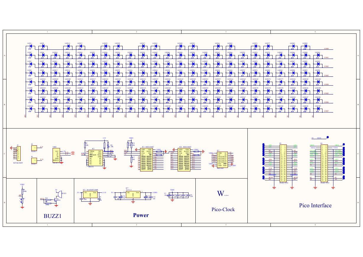 原理图(Pico-Clock-Green-Schdoc).pdf
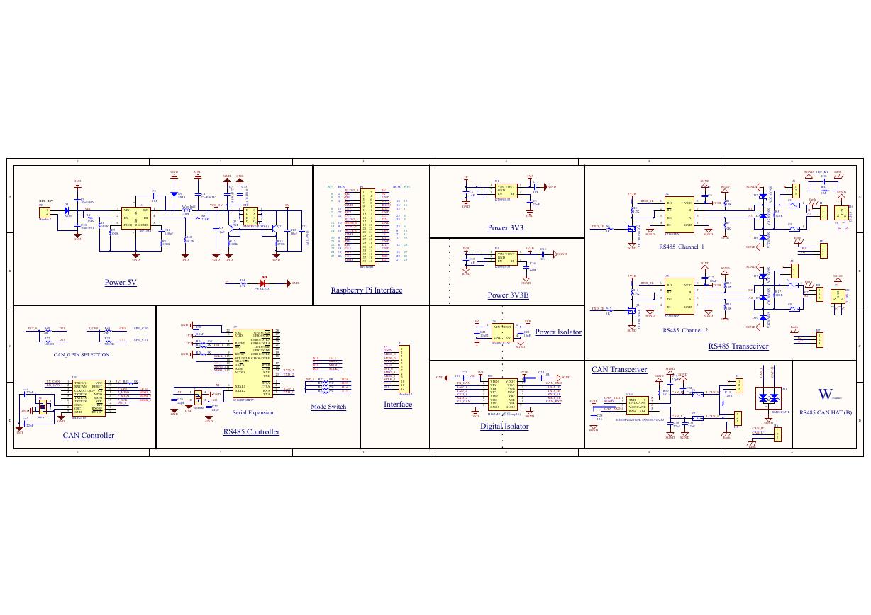 原理图(RS485-CAN-HAT-B-schematic).pdf
 File:SIM7500_SIM7600_SIM7800 Series_SSL_Application Note_V2.00.pdf
 ADS1263(Ads1262).pdf
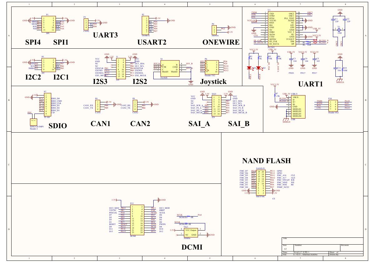 原理图(Open429Z-D-Schematic).pdf
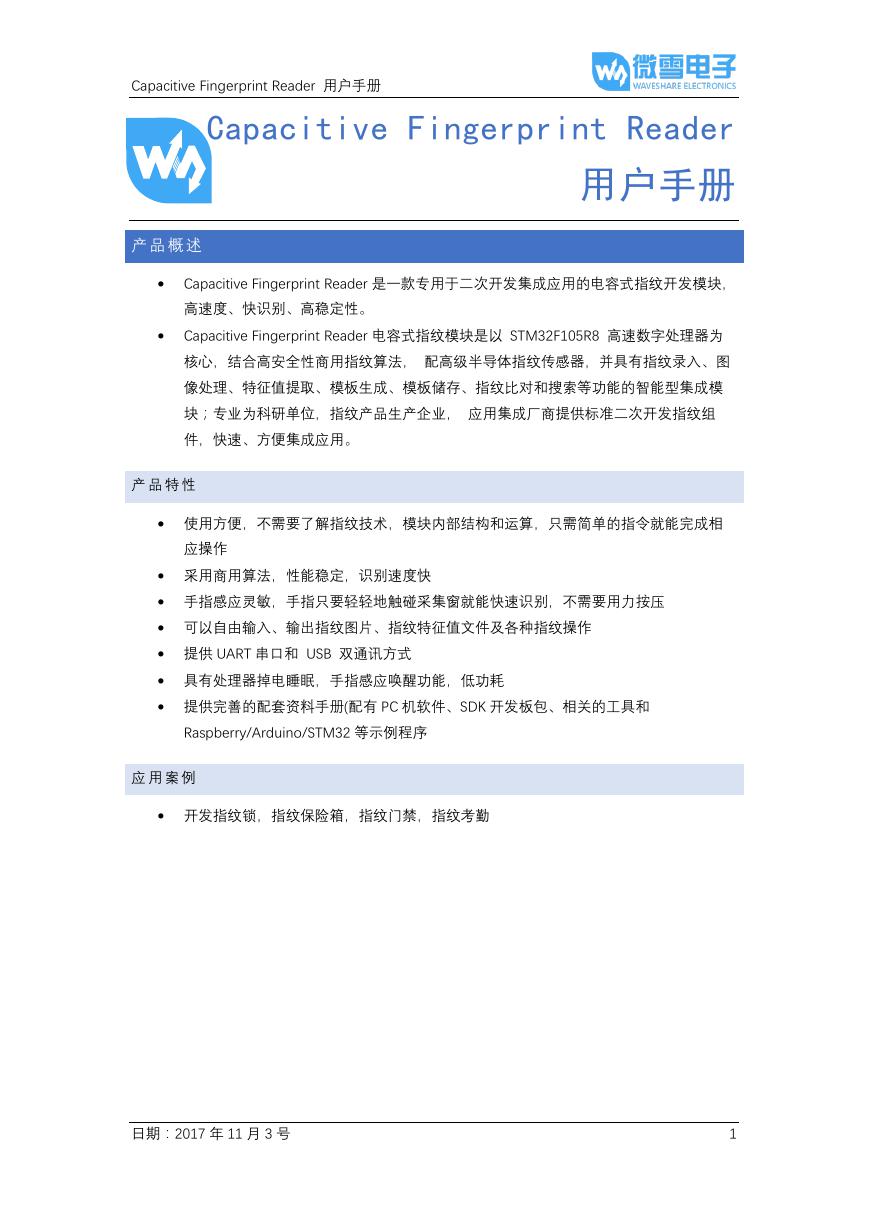 用户手册(Capacitive_Fingerprint_Reader_User_Manual_CN).pdf
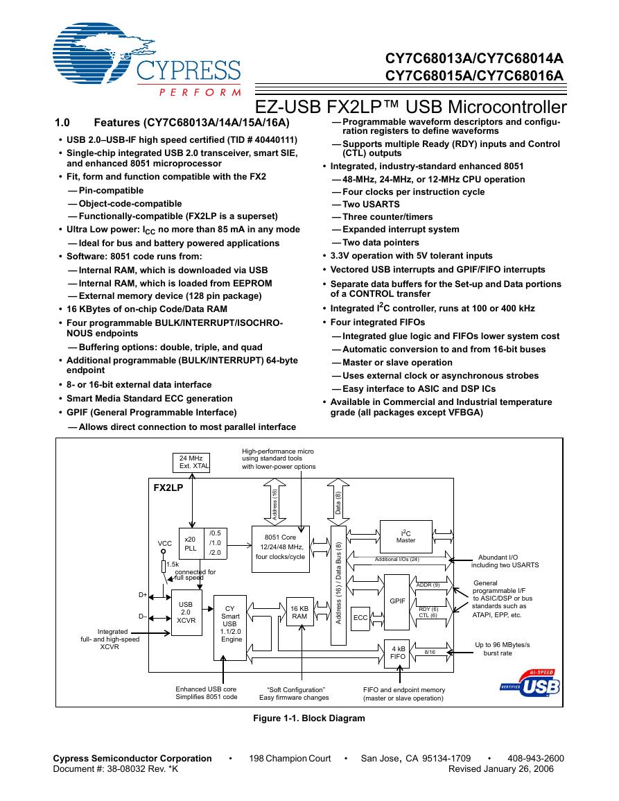 CY7C68013A(英文版)(CY7C68013A).pdf
 TechnicalReference_Dem.pdf