MP1584
3A, 1.5MHz, 28V
Step-Down Converter
FEATURES
Wide 4.5V to 28V Operating Input Range
Programmable Switching Frequency from
100kHz to 1.5MHz
High-Efficiency Pulse Skipping Mode for
Light Load
Ceramic Capacitor Stable
Internal Soft-Start
Internally Set Current Limit without a
Current Sensing Resistor
Available in SOIC8E Package.
APPLICATIONS
High Voltage Power Conversion
Automotive Systems
Distributed Power Systems
Battery Powered Systems
“MPS” and “The Future of Analog IC Technology” are Registered Trademarks of
Monolithic Power Systems, Inc.
Industrial Power Systems
The Future of Analog IC Technology
DESCRIPTION
The MP1584 is a high frequency step-down
switching regulator with an integrated internal
high-side high voltage power MOSFET.
It
provides 3A output with current mode control for
fast loop response and easy compensation.
The wide 4.5V to 28V input range accommodates
a variety of step-down applications, including
those in an automotive input environment. A
100µA operational quiescent current allows use in
battery-powered applications.
High power conversion efficiency over a wide
load range is achieved by scaling down the
switching frequency at light load condition to
reduce the switching and gate driving losses.
The frequency foldback helps prevent inductor
thermal
current runaway during startup and
shutdown provides
fault
tolerant
operation.
By switching at 1.5MHz, the MP1584 is able to
prevent EMI (Electromagnetic Interference) noise
problems, such as those found in AM radio and
ADSL applications.
The MP1584 is available in a thermally enhanced
SOIC8E package.
reliable,
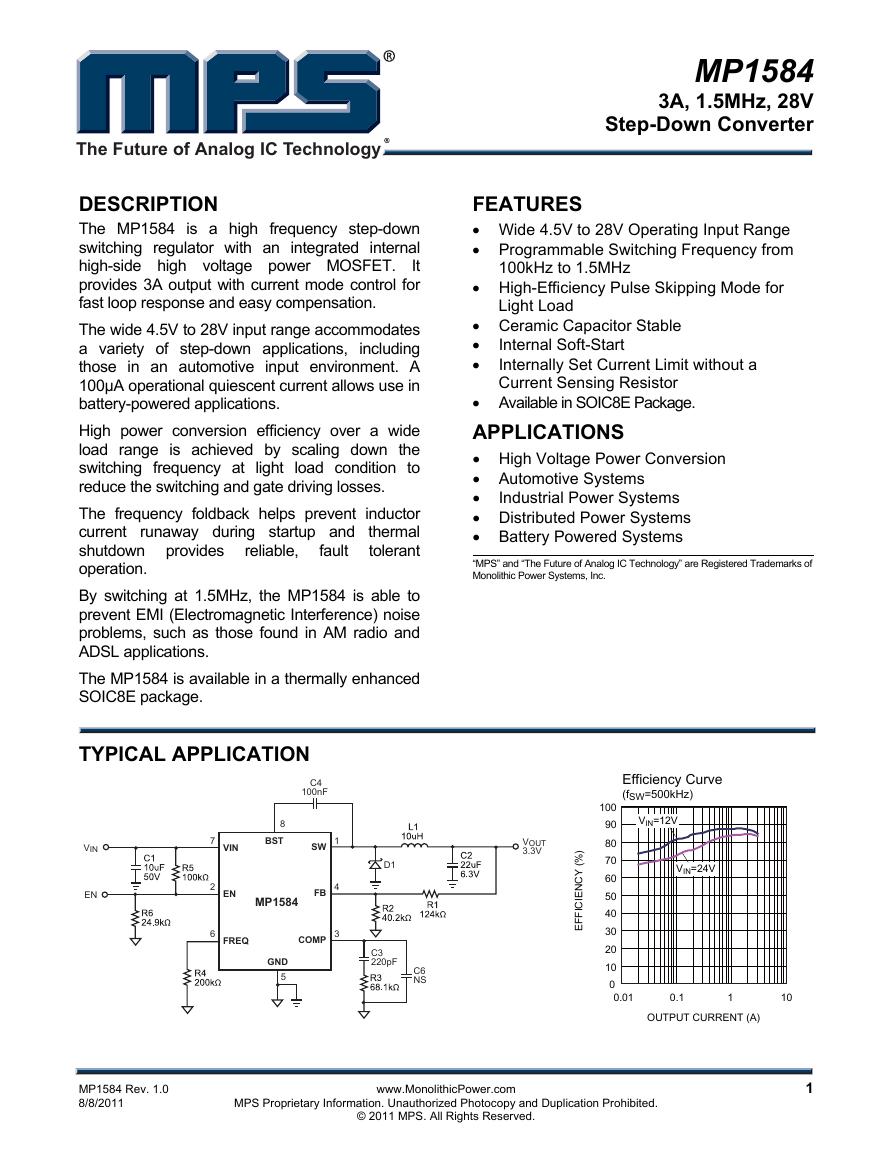
TYPICAL APPLICATION
C4
100nF
SW
FB
8
BST
MP1584
VIN
EN
FREQ
COMP
GND
5
1
4
3
7
2
6
D1
C3
220pF
C6
NS
VOUT
3.3V
)
%
(
I
Y
C
N
E
C
F
F
E
I
Efficiency Curve
(fSW=500kHz)
100
90
80
70
60
50
40
30
20
10
0
0.01
VIN=12V
VIN=24V
0.1
1
OUTPUT CURRENT (A)
10
MPS Proprietary Information. Unauthorized Photocopy and Duplication Prohibited.
www.MonolithicPower.com
© 2011 MPS. All Rights Reserved.
VIN
EN
MP1584 Rev. 1.0
8/8/2011
1
�
MP1584 – 3A, 1.5MHz, 28V STEP-DOWN CONVERTER
ORDERING INFORMATION
Part Number*
MP1584EN
Package
SOIC8E
Top Marking
MP1584EN
Free Air Temperature (TA)
–20C to +85C
* For Tape & Reel, add suffix –Z (e.g. MP1584EN–Z);
For RoHS Compliant Packaging, add suffix –LF. (e.g. MP1584EN–LF–Z)
PACKAGE REFERENCE
TOP VIEW
SW
EN
COMP
FB
1
2
3
4
8
7
6
5
BST
VIN
FREQ
GND
ABSOLUTE MAXIMUM RATINGS (1)
Supply Voltage (VIN) ..................... –0.3V to +30V
Switch Voltage (VSW) ............ –0.3V to VIN + 0.3V
BST to SW ..................................... –0.3V to +6V
All Other Pins ................................. –0.3V to +6V
Continuous Power Dissipation (TA =
+25°C)(2)
............................................................. 2.5W
Junction Temperature ............................... 150C
Lead Temperature .................................... 260C
Storage Temperature .............. –65°C to +150C
Recommended Operating Conditions (3)
Supply Voltage VIN ........................... 4.5V to 28V
Output Voltage VOUT ......................... 0.8V to 25V
Operating Junct. Temp (TJ) ..... –20C to +125C
Thermal Resistance (4)
SOIC8E .................................. 50 ...... 10 ... C/W
θJC
θJA
Notes:
1) Exceeding these ratings may damage the device.
2) The maximum allowable power dissipation is a function of the
maximum junction temperature TJ(MAX), the junction-to-
ambient thermal resistance θJA, and the ambient temperature
TA. The maximum allowable continuous power dissipation at
any ambient temperature is calculated by PD(MAX)=(TJ(MAX)-
TA)/ θJA. Exceeding the maximum allowable power dissipation
will cause excessive die temperature, and the regulator will go
into thermal shutdown. Internal thermal shutdown circuitry
protects the device from permanent damage.
3) The device is not guaranteed to function outside of its
operating conditions.
4) Measured on JESD51-7, 4-layer PCB.
MP1584 Rev. 1.0
8/8/2011
MPS Proprietary Information. Unauthorized Photocopy and Duplication Prohibited.
www.MonolithicPower.com
© 2011 MPS. All Rights Reserved.
2
�
MP1584 – 3A, 1.5MHz, 28V STEP-DOWN CONVERTER
GCS
VFB
4.5V < VIN < 28V
RDS(ON) VBST – VSW = 5V
Symbol Condition
VEN = 0V, VSW = 0V, VIN = 28V
ELECTRICAL CHARACTERISTICS
VIN = 12V, VEN = 2.5V, VCOMP = 1.4V, TA= +25C, unless otherwise noted.
Parameter
Feedback Voltage
Upper Switch On Resistance
Upper Switch Leakage
Current Limit
COMP to Current Sense
Transconductance
Error Amp Voltage Gain (5)
Error Amp Transconductance
Error Amp Min Source current
Error Amp Min Sink current
VIN UVLO Threshold
VIN UVLO Hysteresis
Soft-Start Time (5)
Oscillator Frequency
Shutdown Supply Current
Quiescent Supply Current
Thermal Shutdown
Thermal Shutdown Hysteresis
Minimum Off Time (5)
Minimum On Time (5)
EN Up Threshold
EN Hysteresis
Note:
5) Guaranteed by design.
ICOMP = ±3µA
VFB = 0.7V
VFB = 0.9V
0V < VFB < 0.8V
RFREQ = 100kΩ
VEN = 0V
No load, VFB = 0.9V
Min
0.776
4.0
40
2.7
1.35
MP1584 Rev. 1.0
8/8/2011
MPS Proprietary Information. Unauthorized Photocopy and Duplication Prohibited.
www.MonolithicPower.com
© 2011 MPS. All Rights Reserved.
0.824
Typ Max Units
V
0.8
mΩ
150
μA
1
4.7
A
9
200
60
5
–5
3.0
0.35
1.5
900
12
100
150
15
100
100
1.5
300
80
3.3
20
125
1.65
A/V
V/V
µA/V
µA
µA
V
V
ms
kHz
µA
µA
C
C
ns
ns
V
mV
3
�
MP1584 – 3A, 1.5MHz, 28V STEP-DOWN CONVERTER
PIN FUNCTIONS
SOIC
Pin # Name Description
1
SW
2
3
4
5
6
7
8
Switch Node. This is the output from the high-side switch. A low forward drop Schottky diode to
ground is required. The diode must be close to the SW pins to reduce switching spikes.
Enable Input. Pulling this pin below the specified threshold shuts the chip down. Pulling it up
above the specified threshold or leaving it floating enables the chip.
EN
COMP Compensation. This node is the output of the error amplifier. Control loop frequency
compensation is applied to this pin.
Feedback. This is the input to the error amplifier. The output voltage is set by a resistive divider
connected between the output and GND which scales down VOUT equal to the internal +0.8V
reference.
FB
GND
Exposed
Ground. It should be connected as close as possible to the output capacitor to shorten the high
current switch paths. Connect exposed pad to GND plane for optimal thermal performance.
Pad
FREQ Switching Frequency Program Input. Connect a resistor from this pin to ground to set the
switching frequency.
Input Supply. This supplies power to all the internal control circuitry, both BS regulators and the
high-side switch. A decoupling capacitor to ground must be placed close to this pin to minimize
switching spikes.
VIN
BST Bootstrap. This is the positive power supply for the internal floating high-side MOSFET driver.
Connect a bypass capacitor between this pin and SW pin.
MP1584 Rev. 1.0
8/8/2011
MPS Proprietary Information. Unauthorized Photocopy and Duplication Prohibited.
www.MonolithicPower.com
© 2011 MPS. All Rights Reserved.
4
�
MP1584 – 3A, 1.5MHz, 28V STEP-DOWN CONVERTER
TYPICAL PERFORMANCE CHARACTERISTICS
VIN = 12V, VOUT=5V, C1 = 10µF, C2 = 22µF, L1= 10µH, TA = +25C, unless otherwise noted.
Oscillating Frequency
vs. Rfreq
)
Z
H
k
(
Y
C
N
E
U
Q
E
R
F
G
N
T
A
L
L
C
S
O
I
I
1600
1400
1200
1000
800
600
400
200
0
10
100
1000
10000
Steady State
IOUT=0.1A, fSW=500kHz
Steady State
IOUT=1A, fSW=500kHz
Steady State
IOUT=2A, fSW=500kHz
VOUT
AC Coupled
10mV/div.
VSW
10V/div.
IL
1A/div.
1
v.
VOUT
AC Coupled
10mV/div.
VSW
10V/div.
IL
1A/div.
VOUT
AC Coupled
10mV/div.
VSW
10V/div.
IL
2A/div.
2
v.
2
v.
MP1584 Rev. 1.0
8/8/2011
MPS Proprietary Information. Unauthorized Photocopy and Duplication Prohibited.
www.MonolithicPower.com
© 2011 MPS. All Rights Reserved.
5
�
MP1584 – 3A, 1.5MHz, 28V STEP-DOWN CONVERTER
TYPICAL PERFORMANCE CHARACTERISTICS (continued)
VIN = 12V, C1 = 10µF, C2 = 22µF, L1 = 10µH, fSW=500kHz, and TA = +25C, unless otherwise noted.
Startup
IOUT = 0.1A
Shutdown
IOUT = 0.1A
Startup
IOUT = 1A
VEN
5V/div.
VOUT
2V/div.
VSW
10V/div.
IL
1A/div.
VEN
5V/div.
VOUT
2V/div.
VSW
10V/div.
IL
1A/div.
VOUT
2V/div.
IL
1A/div.
VEN
5V/div.
VOUT
2V/div.
VSW
10V/div.
IL
1A/div.
VEN
5V/div.
VOUT
2V/div.
VSW
10V/div.
IL
1A/div.
5ms/div.
1ms/div.
5ms/div.
Shutdown
IOUT = 1A
Startup
IOUT = 2A
Shutdown
IOUT = 2A
VEN
5V/div.
VOUT
2V/div.
VSW
10V/div.
IL
2A/div.
5ms/div.
VEN
5V/div.
VOUT
2V/div.
VSW
10V/div.
IL
2A/div.
Short Circuit Entry
IOUT = 0.1A to Short
Short Circuit Recovery
IOUT = Short to 0.1A
VOUT
2V/div.
IL
1A/div.
MP1584 Rev. 1.0
8/8/2011
MPS Proprietary Information. Unauthorized Photocopy and Duplication Prohibited.
www.MonolithicPower.com
© 2011 MPS. All Rights Reserved.
6
�
BLOCK DIAGRAM
MP1584 – 3A, 1.5MHz, 28V STEP-DOWN CONVERTER
VIN
VIN
EN
VOUT
FB
REFERENCE UVLO/
THERMAL
SHUTDOWN
INTERNAL
REGULATORS
+
--
--+
5V
2.6V
SW
1.5ms SS
SS
Gm Error Amp
SS
0V8
--
+
ISW
--
+
Level
Shift
COMP
OSCILLATOR
CLK
BST
SW
ISW
COMP
GND
FREQ
Figure 1—Functional Block Diagram
VOUT
is a
variable
step-down
OPERATION
frequency,
The MP1584
non-synchronous,
switching
regulator with an integrated high-side high
voltage power MOSFET. It provides a highly
efficient solution with current mode control for
fast loop response and easy compensation. It
features a wide input voltage range, internal
soft-start control and precision current limiting.
low operational quiescent current
Its very
makes
it suitable
for battery powered
applications.
PWM Control
At moderate to high output current, the MP1584
operates in a fixed frequency, peak current
control mode to regulate the output voltage. A
PWM cycle is initiated by the internal clock. The
power MOSFET is turned on and remains on
until its current reaches the value set by the
COMP voltage. When the power switch is off, it
remains off for at least 100ns before the next
cycle starts. If, in one PWM period, the current
in the power MOSFET does not reach the
COMP set current value, the power MOSFET
remains on, saving a turn-off operation.
MP1584 Rev. 1.0
8/8/2011
MPS Proprietary Information. Unauthorized Photocopy and Duplication Prohibited.
www.MonolithicPower.com
© 2011 MPS. All Rights Reserved.
7
�
MP1584 – 3A, 1.5MHz, 28V STEP-DOWN CONVERTER
Error Amplifier
The error amplifier compares the FB pin voltage
with the internal reference (REF) and outputs a
current proportional to the difference between
the two. This output current is then used to
charge the external compensation network to
form the COMP voltage, which is used to
control the power MOSFET current.
During operation, the minimum COMP voltage
is clamped to 0.9V and its maximum is clamped
to 2.0V. COMP is internally pulled down to GND
in shutdown mode. COMP should not be pulled
up beyond 2.6V.
Internal Regulator
Most of the internal circuitries are powered from
the 2.6V internal regulator. This regulator takes
the VIN input and operates in the full VIN range.
When VIN is greater than 3.0V, the output of
the regulator is in full regulation. When VIN is
lower than 3.0V, the output decreases.
Enable Control
The MP1584 has a dedicated enable control pin
(EN). With high enough input voltage, the chip
can be enabled and disabled by EN which has
positive logic. Its falling threshold is a precision
1.2V, and its rising threshold is 1.5V (300mV
higher).
When floating, EN is pulled up to about 3.0V by
an internal 1µA current source so it is enabled.
To pull it down, 1µA current capability is
needed.
When EN is pulled down below 1.2V, the chip is
put into the lowest shutdown current mode.
When EN is higher than zero but lower than its
rising threshold, the chip is still in shutdown
mode but
increases
slightly.
Under-Voltage Lockout (UVLO)
Under-voltage lockout (UVLO) is implemented
to protect the chip from operating at insufficient
supply voltage. The UVLO rising threshold is
about 3.0V while its falling threshold is a
consistent 2.6V.
the shutdown current
the chip starts,
Internal Soft-Start
The soft-start is implemented to prevent the
from overshooting
converter output voltage
during startup. When
the
internal circuitry generates a soft-start voltage
(SS) ramping up from 0V to 2.6V. When it is
lower than the internal reference (REF), SS
overrides REF so the error amplifier uses SS as
the reference. When SS is higher than REF,
REF regains control.
Thermal Shutdown
Thermal shutdown is implemented to prevent
the chip from operating at exceedingly high
temperatures. When the silicon die temperature
is higher than its upper threshold, it shuts down
the whole chip. When the temperature is lower
than its lower threshold, the chip is enabled
again.
Floating Driver and Bootstrap Charging
The floating power MOSFET driver is powered
by an external bootstrap capacitor. This floating
driver has
its own UVLO protection. This
UVLO’s rising threshold is 2.2V with a threshold
of 150mV.
The bootstrap capacitor
is charged and
regulated to about 5V by the dedicated internal
bootstrap regulator. When the voltage between
the BST and SW nodes is lower than its
regulation, a PMOS pass transistor connected
from VIN to BST is turned on. The charging
current path is from VIN, BST and then to SW.
External circuit should provide enough voltage
headroom to facilitate the charging.
As long as VIN is sufficiently higher than SW,
the bootstrap capacitor can be charged. When
the power MOSFET is ON, VIN is about equal
to SW so the bootstrap capacitor cannot be
charged. When the external diode is on, the
difference between VIN and SW is largest, thus
making it the best period to charge. When there
is no current in the inductor, SW equals the
output voltage VOUT so the difference between
VIN and VOUT can be used to charge the
bootstrap capacitor.
MP1584 Rev. 1.0
8/8/2011
MPS Proprietary Information. Unauthorized Photocopy and Duplication Prohibited.
www.MonolithicPower.com
© 2011 MPS. All Rights Reserved.
8
�


 V2版本原理图(Capacitive-Fingerprint-Reader-Schematic_V2).pdf
 摄像头工作原理.doc
 VL53L0X简要说明(En.FLVL53L00216).pdf
 原理图(DVK720-Schematic).pdf
 原理图(Pico-Clock-Green-Schdoc).pdf
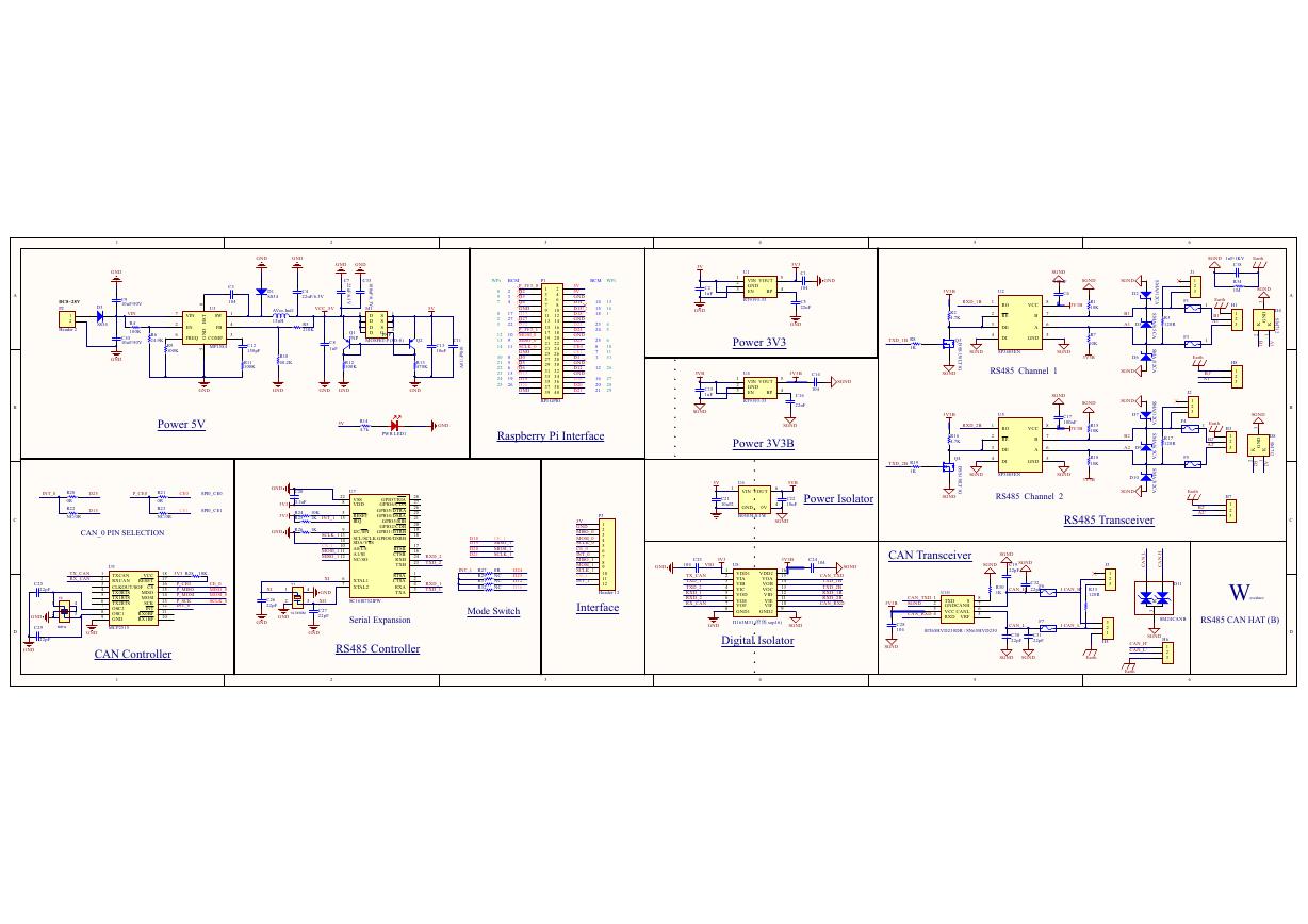 原理图(RS485-CAN-HAT-B-schematic).pdf
 File:SIM7500_SIM7600_SIM7800 Series_SSL_Application Note_V2.00.pdf
 ADS1263(Ads1262).pdf
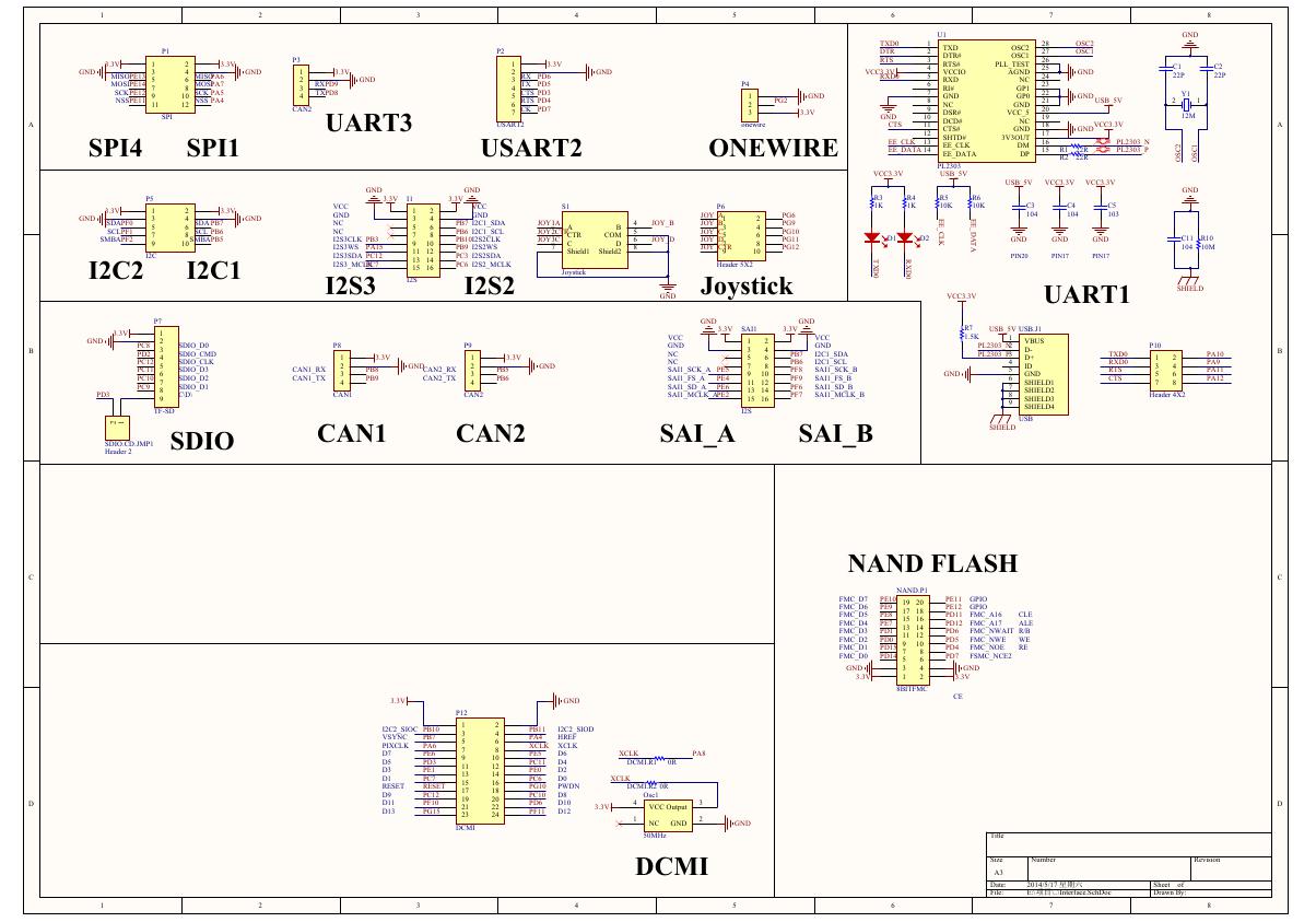 原理图(Open429Z-D-Schematic).pdf
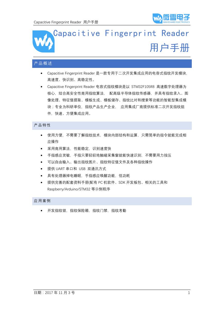 用户手册(Capacitive_Fingerprint_Reader_User_Manual_CN).pdf
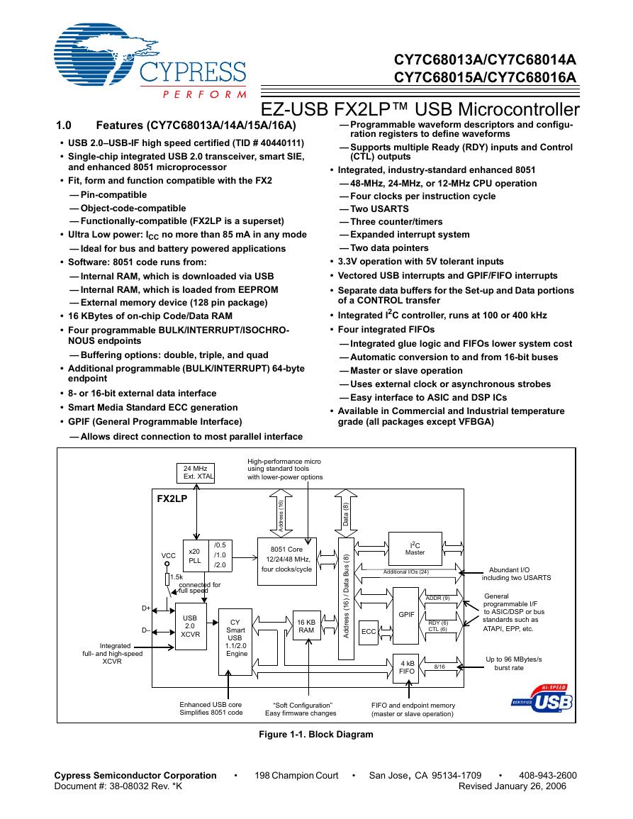 CY7C68013A(英文版)(CY7C68013A).pdf
 TechnicalReference_Dem.pdf