PCA9685
16-channel, 12-bit PWM Fm+ I2C-bus LED controller
Rev. 02 — 16 July 2009
Product data sheet
1. General description
The PCA9685 is an I2C-bus controlled 16-channel LED controller optimized for LCD
Red/Green/Blue/Amber (RGBA) color backlighting applications. Each LED output has its
own 12-bit resolution (4096 steps) fixed frequency individual PWM controller that operates
at a programmable frequency from a typical of 40 Hz to 1000 Hz with a duty cycle that is
adjustable from 0 % to 100 % to allow the LED to be set to a specific brightness value.
All outputs are set to the same PWM frequency.
Each LED output can be off or on (no PWM control), or set at its individual PWM controller
value. The LED output driver is programmed to be either open-drain with a 25 mA current
sink capability at 5 V or totem pole with a 25 mA sink, 10 mA source capability at 5 V. The
PCA9685 operates with a supply voltage range of 2.3 V to 5.5 V and the inputs and
outputs are 5.5 V tolerant. LEDs can be directly connected to the LED output (up to
25 mA, 5.5 V) or controlled with external drivers and a minimum amount of discrete
components for larger current or higher voltage LEDs.
The PCA9685 is in the new Fast-mode Plus (Fm+) family. Fm+ devices offer higher
frequency (up to 1 MHz) and more densely populated bus operation (up to 4000 pF).
Although the PCA9635 and PCA9685 have many similar features, the PCA9685 has
some unique features that make it more suitable for applications such as LCD backlighting
and Ambilight:
• The PCA9685 allows staggered LED output on and off times to minimize current
surges. The on and off time delay is independently programmable for each of the
16 channels. This feature is not available in PCA9635.
• The PCA9685 has 4096 steps (12-bit PWM) of individual LED brightness control. The
PCA9635 has only 256 steps (8-bit PWM).
• When multiple LED controllers are incorporated in a system, the PWM pulse widths
between multiple devices may differ if PCA9635s are used. The PCA9685 has a
programmable prescaler to adjust the PWM pulse widths of multiple devices.
• The PCA9685 has an external clock input pin that will accept user-supplied clock
(50 MHz max.) in place of the internal 25 MHz oscillator. This feature allows
synchronization of multiple devices. The PCA9635 does not have external clock input
feature.
• Like the PCA9635, PCA9685 also has a built-in oscillator for the PWM control.
However, the frequency used for PWM control in the PCA9685 is adjustable from
about 40 Hz to 1000 Hz as compared to the typical 97.6 kHz frequency of the
PCA9635. This allows the use of PCA9685 with external power supply controllers. All
bits are set at the same frequency.
• The Power-On Reset (POR) default state of LEDn output pins is LOW in the case of
PCA9685. It is HIGH for PCA9635.
�
NXP Semiconductors
PCA9685
16-channel, 12-bit PWM Fm+ I2C-bus LED controller
2. Features
The active LOW Output Enable input pin (OE) allows asynchronous control of the LED
outputs and can be used to set all the outputs to a defined I2C-bus programmable logic
state. The OE can also be used to externally ‘pulse width modulate’ the outputs, which is
useful when multiple devices need to be dimmed or blinked together using software
control.
Software programmable LED All Call and three Sub Call I2C-bus addresses allow all or
defined groups of PCA9685 devices to respond to a common I2C-bus address, allowing
for example, all red LEDs to be turned on or off at the same time or marquee chasing
effect, thus minimizing I2C-bus commands. Six hardware address pins allow up to
62 devices on the same bus.
The Software Reset (SWRST) General Call allows the master to perform a reset of the
PCA9685 through the I2C-bus, identical to the Power-On Reset (POR) that initializes the
registers to their default state causing the outputs to be set LOW. This allows an easy and
quick way to reconfigure all device registers to the same condition via software.
n 16 LED drivers. Each output programmable at:
u Off
u On
u Programmable LED brightness
u Programmable LED turn-on time to help reduce EMI
n 1 MHz Fast-mode Plus compatible I2C-bus interface with 30 mA high drive capability
on SDA output for driving high capacitive buses
n 4096-step (12-bit) linear programmable brightness per LED output varying from fully
off (default) to maximum brightness
n LED output frequency (all LEDs) typically varies from 40 Hz to 1000 Hz (Default of 1Eh
in PRE_SCALE register results in a 200 Hz refresh rate with oscillator clock of
25 MHz.)
n Sixteen totem pole outputs (sink 25 mA and source 10 mA at 5 V) with software
programmable open-drain LED outputs selection (default at totem pole). No input
function.
n Output state change programmable on the Acknowledge or the STOP Command to
update outputs byte-by-byte or all at the same time (default to ‘Change on STOP’).
n Active LOW Output Enable (OE) input pin. LEDn outputs programmable to logic 1,
logic 0 (default at power-up) or ‘high-impedance’ when OE is HIGH.
n 6 hardware address pins allow 62 PCA9685 devices to be connected to the same
I2C-bus
n Toggling OE allows for hardware LED blinking
n 4 software programmable I2C-bus addresses (one LED All Call address and three LED
Sub Call addresses) allow groups of devices to be addressed at the same time in any
combination (for example, one register used for ‘All Call’ so that all the PCA9685s on
the I2C-bus can be addressed at the same time and the second register used for three
different addresses so that 1⁄3 of all devices on the bus can be addressed at the same
time in a group). Software enable and disable for these I2C-bus address.
n Software Reset feature (SWRST General Call) allows the device to be reset through
the I2C-bus
PCA9685_2
Product data sheet
Rev. 02 — 16 July 2009
© NXP B.V. 2009. All rights reserved.
2 of 50
�
NXP Semiconductors
PCA9685
16-channel, 12-bit PWM Fm+ I2C-bus LED controller
n 25 MHz typical internal oscillator requires no external components
n External 50 MHz (max.) clock input
n Internal power-on reset
n Noise filter on SDA/SCL inputs
n Edge rate control on outputs
n No output glitches on power-up
n Supports hot insertion
n Low standby current
n Operating power supply voltage range of 2.3 V to 5.5 V
n 5.5 V tolerant inputs
n - 40 C to +85 C operation
n ESD protection exceeds 2000 V HBM per JESD22-A114, 200 V MM per
JESD22-A115 and 1000 V CDM per JESD22-C101
n Latch-up testing is done to JEDEC Standard JESD78 which exceeds 100 mA
n Packages offered: TSSOP28, HVQFN28
3. Applications
n RGB or RGBA LED drivers
n LED status information
n LED displays
n LCD backlights
n Keypad backlights for cellular phones or handheld devices
4. Ordering information
Table 1.
Type number
Ordering information
Topside mark
PCA9685PW
PCA9685PW
Package
Name
TSSOP28
PCA9685PW/Q900[1]
PCA9685PW
TSSOP28
PCA9685BS
PCA9685BS
HVQFN28
Description
plastic thin shrink small outline package;
28 leads; body width 4.4 mm
plastic thin shrink small outline package;
28 leads; body width 4.4 mm
plastic thermal enhanced very thin quad flat
package; no leads; 28 terminals;
body 6 · 6 · 0.85 mm
Version
SOT361-1
SOT361-1
SOT788-1
[1] PCA9685PW/Q900 is AEC-Q100 compliant. Contact i2c.support@nxp.com for PPAP.
PCA9685_2
Product data sheet
Rev. 02 — 16 July 2009
© NXP B.V. 2009. All rights reserved.
3 of 50
�
NXP Semiconductors
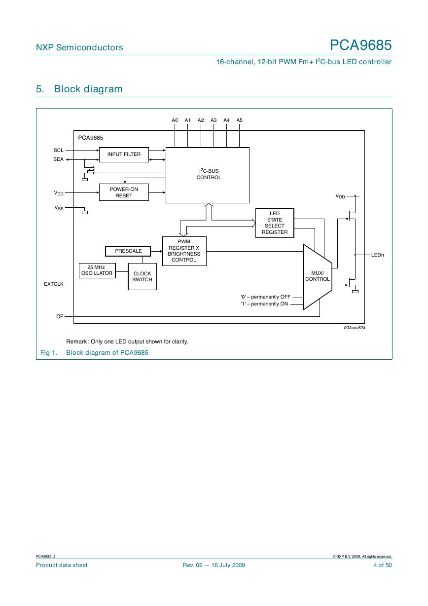
5. Block diagram
PCA9685
16-channel, 12-bit PWM Fm+ I2C-bus LED controller
A0
A1
A2
A3
A4
A5
I2C-BUS
CONTROL
PCA9685
INPUT FILTER
POWER-ON
RESET
VDD
LED
STATE
SELECT
REGISTER
PWM
REGISTER X
BRIGHTNESS
CONTROL
PRESCALE
25 MHz
OSCILLATOR
CLOCK
SWITCH
'0' – permanently OFF
'1' – permanently ON
LEDn
MUX/
CONTROL
002aac824
SCL
SDA
VDD
VSS
EXTCLK
OE
Remark: Only one LED output shown for clarity.
Fig 1. Block diagram of PCA9685
PCA9685_2
Product data sheet
Rev. 02 — 16 July 2009
© NXP B.V. 2009. All rights reserved.
4 of 50
�
NXP Semiconductors
6. Pinning information
6.1 Pinning
PCA9685
16-channel, 12-bit PWM Fm+ I2C-bus LED controller
A0
A1
A2
A3
A4
LED0
LED1
LED2
LED3
LED4
LED5
LED6
LED7
VSS
1
2
3
4
5
6
7
8
9
10
11
12
13
14
28
27
26
25
24
23
22
21
20
19
18
17
16
15
VDD
SDA
SCL
EXTCLK
A5
OE
LED15
LED14
LED13
LED12
LED11
LED10
LED9
LED8
PCA9685PW
PCA9685PW/Q900
002aac825
terminal 1
index area
2
A
1
A
0
A
D
D
V
A
D
S
L
C
S
K
L
C
T
X
E
8
2
7
2
6
2
5
2
4
2
3
2
2
2
A3
A4
LED0
LED1
LED2
LED3
LED4
1
2
3
4
5
6
7
PCA9685BS
0
8 9 1
1
1
2
1
3
1
4
1
5
D
E
L
6
D
E
L
7
D
E
L
S
S
V
8
D
E
L
9
D
E
L
0
1
D
E
L
Transparent top view
21
20
19
18
17
16
15
A5
OE
LED15
LED14
LED13
LED12
LED11
002aad236
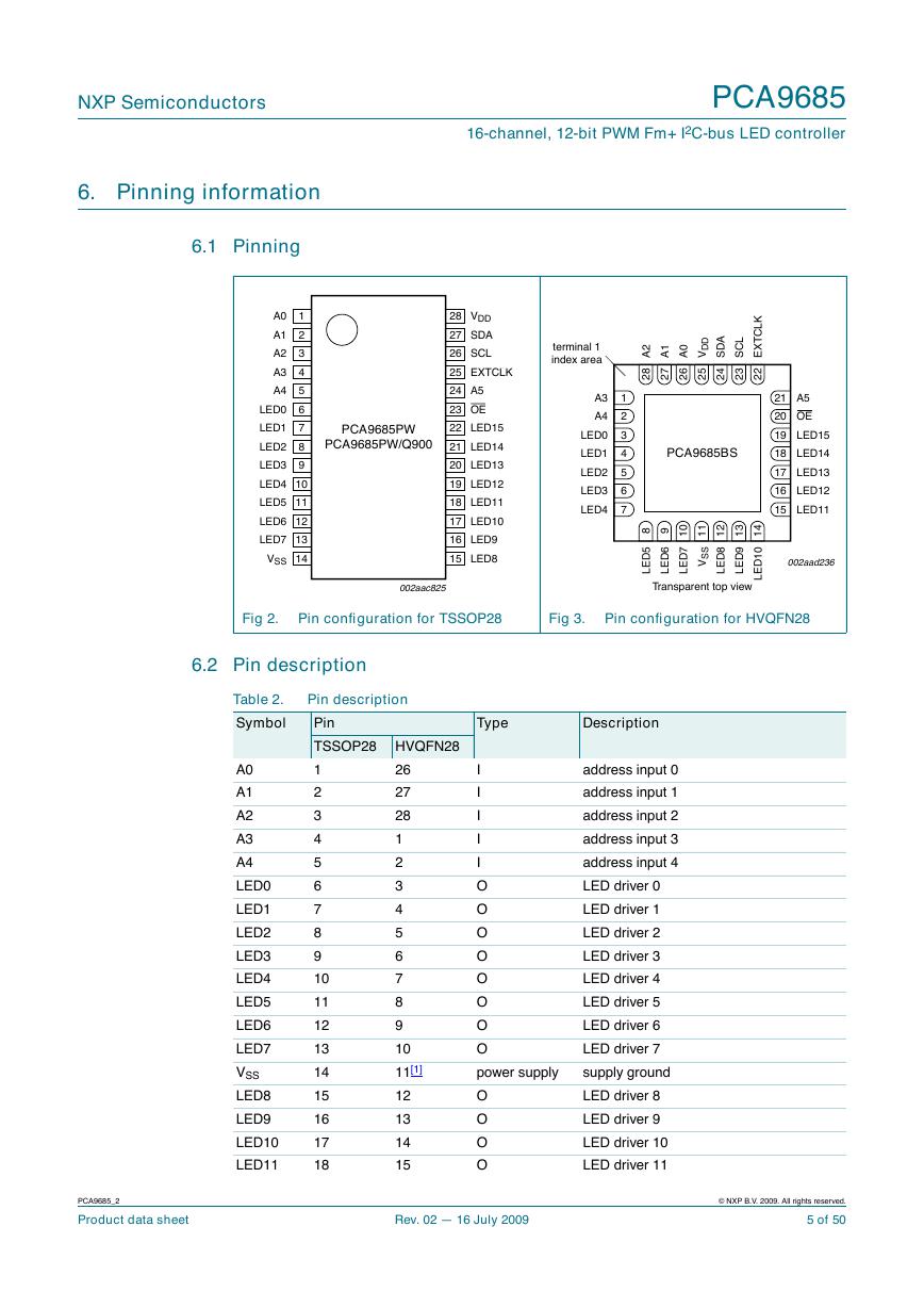
Fig 2.
Pin configuration for TSSOP28
Fig 3.
Pin configuration for HVQFN28
6.2 Pin description
Table 2.
Symbol
A0
A1
A2
A3
A4
LED0
LED1
LED2
LED3
LED4
LED5
LED6
LED7
VSS
LED8
LED9
LED10
LED11
Pin description
Pin
TSSOP28 HVQFN28
1
2
3
4
5
6
7
8
9
10
11
12
13
14
15
16
17
18
26
27
28
1
2
3
4
5
6
7
8
9
10
11[1]
12
13
14
15
Type
Description
I
I
I
I
I
O
O
O
O
O
O
O
O
power supply
O
O
O
O
address input 0
address input 1
address input 2
address input 3
address input 4
LED driver 0
LED driver 1
LED driver 2
LED driver 3
LED driver 4
LED driver 5
LED driver 6
LED driver 7
supply ground
LED driver 8
LED driver 9
LED driver 10
LED driver 11
PCA9685_2
Product data sheet
Rev. 02 — 16 July 2009
© NXP B.V. 2009. All rights reserved.
5 of 50
�
NXP Semiconductors
PCA9685
16-channel, 12-bit PWM Fm+ I2C-bus LED controller
Table 2.
Symbol
LED12
LED13
LED14
LED15
OE
A5
EXTCLK
SCL
SDA
VDD
Pin description …continued
Pin
TSSOP28 HVQFN28
19
20
21
22
23
24
25
26
27
28
16
17
18
19
20
21
22
23
24
25
Type
O
O
O
O
I
I
I
I
I/O
power supply
Description
LED driver 12
LED driver 13
LED driver 14
LED driver 15
active LOW output enable
address input 5
external clock input[2]
serial clock line
serial data line
supply voltage
[1] HVQFN28 package die supply ground is connected to both VSS pin and exposed center pad. VSS pin must
be connected to supply ground for proper device operation. For enhanced thermal, electrical, and board
level performance, the exposed pad needs to be soldered to the board using a corresponding thermal pad
on the board and for proper heat conduction through the board, thermal vias need to be incorporated in the
PCB in the thermal pad region.
[2] This pin must be grounded when this feature is not used.
7. Functional description
Refer to Figure 1 “Block diagram of PCA9685”.
7.1 Device addresses
Following a START condition, the bus master must output the address of the slave it is
accessing.
There are a maximum of 64 possible programmable addresses using the 6 hardware
address pins. Two of these addresses, Software Reset and LED All Call, cannot be used
because their default power-up state is ON, leaving a maximum of 62 addresses. Using
other reserved addresses, as well as any other subcall address, will reduce the total
number of possible addresses even further.
7.1.1 Regular I2C-bus slave address
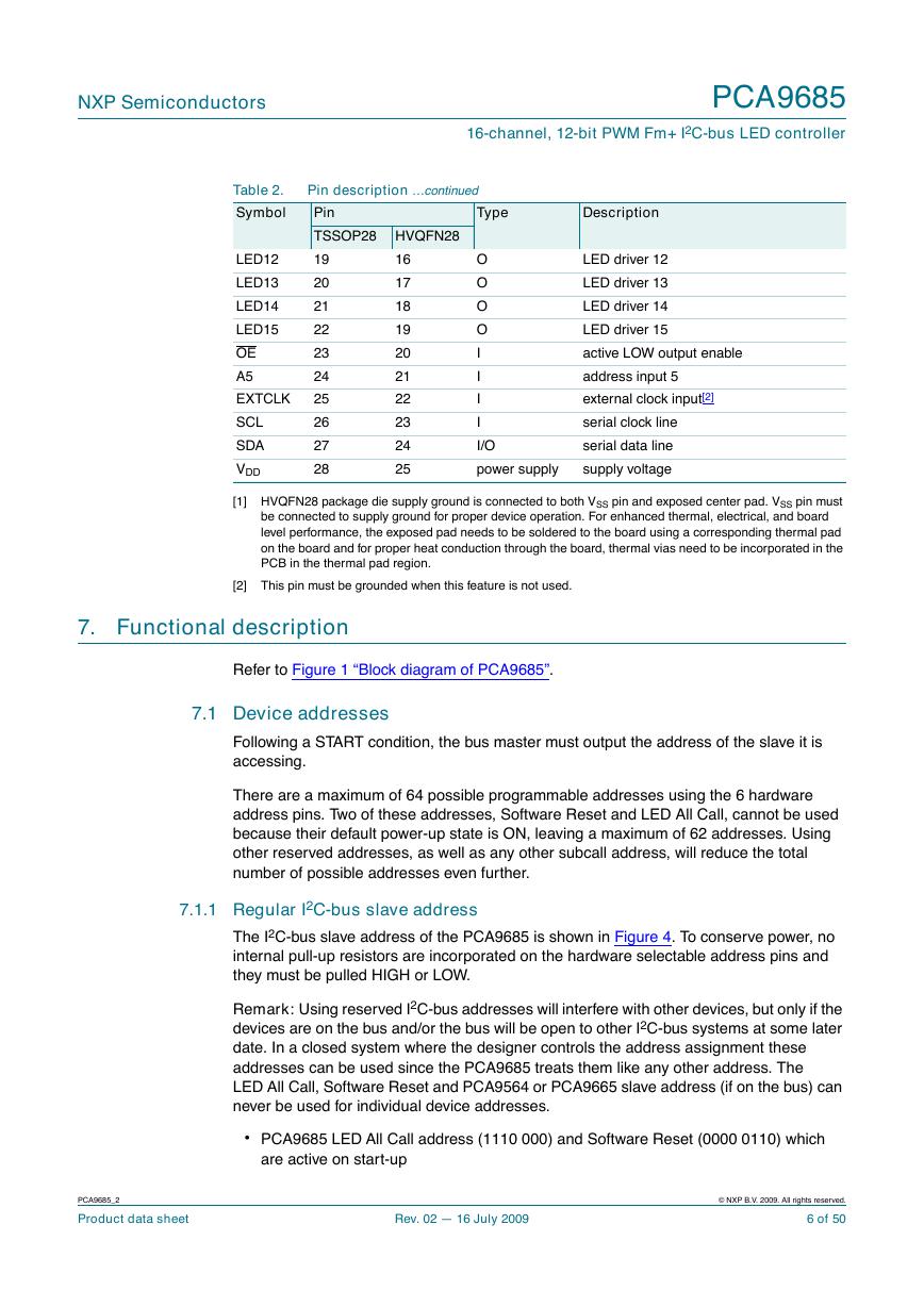
The I2C-bus slave address of the PCA9685 is shown in Figure 4. To conserve power, no
internal pull-up resistors are incorporated on the hardware selectable address pins and
they must be pulled HIGH or LOW.
Remark: Using reserved I2C-bus addresses will interfere with other devices, but only if the
devices are on the bus and/or the bus will be open to other I2C-bus systems at some later
date. In a closed system where the designer controls the address assignment these
addresses can be used since the PCA9685 treats them like any other address. The
LED All Call, Software Reset and PCA9564 or PCA9665 slave address (if on the bus) can
never be used for individual device addresses.
• PCA9685 LED All Call address (1110 000) and Software Reset (0000 0110) which
are active on start-up
PCA9685_2
Product data sheet
Rev. 02 — 16 July 2009
© NXP B.V. 2009. All rights reserved.
6 of 50
�
NXP Semiconductors
PCA9685
16-channel, 12-bit PWM Fm+ I2C-bus LED controller
• PCA9564 (0000 000) or PCA9665 (1110 000) slave address which is active on
start-up
• ‘reserved for future use’ I2C-bus addresses (0000 011, 1111 1XX)
• slave devices that use the 10-bit addressing scheme (1111 0XX)
• slave devices that are designed to respond to the General Call address (0000 000)
which is used as the software reset address
• High-speed mode (Hs-mode) master code (0000 1XX)
slave address
1
A5 A4 A3 A2 A1 A0
R/W
fixed
hardware selectable
002aad168
Fig 4.
Slave address
The last bit of the address byte defines the operation to be performed. When set to logic 1
a read is selected, while a logic 0 selects a write operation.
7.1.2 LED All Call I2C-bus address
• Default power-up value (ALLCALLADR register): E0h or 1110 000X
• Programmable through I2C-bus (volatile programming)
• At power-up, LED All Call I2C-bus address is enabled. PCA9685 sends an ACK when
E0h (R/W = 0) or E1h (R/W = 1) is sent by the master.
See Section 7.3.7 “ALLCALLADR, LED All Call I2C-bus address” for more detail.
Remark: The default LED All Call I2C-bus address (E0h or 1110 000X) must not be used
as a regular I2C-bus slave address since this address is enabled at power-up. All the
PCA9685s on the I2C-bus will acknowledge the address if sent by the I2C-bus master.
7.1.3 LED Sub Call I2C-bus addresses
• 3 different I2C-bus addresses can be used
• Default power-up values:
– SUBADR1 register: E2h or 1110 001X
– SUBADR2 register: E4h or 1110 010X
– SUBADR3 register: E8h or 1110 100X
• Programmable through I2C-bus (volatile programming)
• At power-up, Sub Call I2C-bus addresses are disabled. PCA9685 does not send an
ACK when E2h (R/W = 0) or E3h (R/W = 1), E4h (R/W = 0) or E5h (R/W = 1), or
E8h (R/W = 0) or E9h (R/W = 1) is sent by the master.
See Section 7.3.6 “SUBADR1 to SUBADR3, I2C-bus subaddress 1 to 3” for more detail.
Remark: The default LED Sub Call I2C-bus addresses may be used as regular I2C-bus
slave addresses as long as they are disabled.
PCA9685_2
Product data sheet
Rev. 02 — 16 July 2009
© NXP B.V. 2009. All rights reserved.
7 of 50
�
NXP Semiconductors
PCA9685
16-channel, 12-bit PWM Fm+ I2C-bus LED controller
7.1.4 Software Reset I2C-bus address
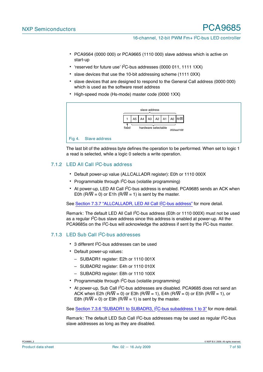
The address shown in Figure 5 is used when a reset of the PCA9685 needs to be
performed by the master. The Software Reset address (SWRST Call) must be used with
R/W = logic 0. If R/W = logic 1, the PCA9685 does not acknowledge the SWRST. See
Section 7.6 “Software reset” for more detail.
R/W
0
0
0
0
0
1
1
0
002aab416
Fig 5.
Software Reset address
Remark: The Software Reset I2C-bus address is a reserved address and cannot be used
as a regular I2C-bus slave address or as an LED All Call or LED Sub Call address.
7.2 Control register
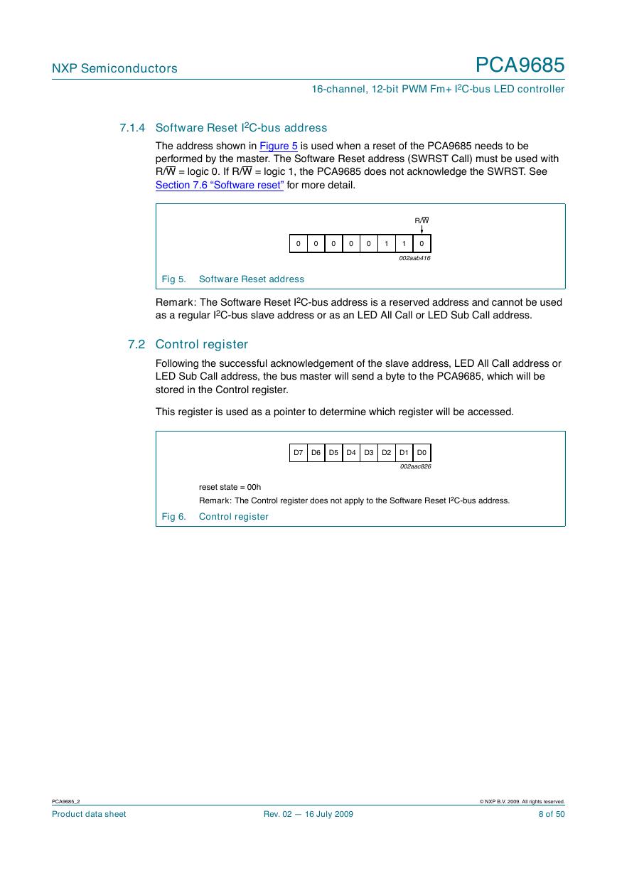
Following the successful acknowledgement of the slave address, LED All Call address or
LED Sub Call address, the bus master will send a byte to the PCA9685, which will be
stored in the Control register.
This register is used as a pointer to determine which register will be accessed.
D7 D6 D5 D4 D3 D2 D1 D0
002aac826
reset state = 00h
Remark: The Control register does not apply to the Software Reset I2C-bus address.
Fig 6. Control register
PCA9685_2
Product data sheet
Rev. 02 — 16 July 2009
© NXP B.V. 2009. All rights reserved.
8 of 50
�


 V2版本原理图(Capacitive-Fingerprint-Reader-Schematic_V2).pdf
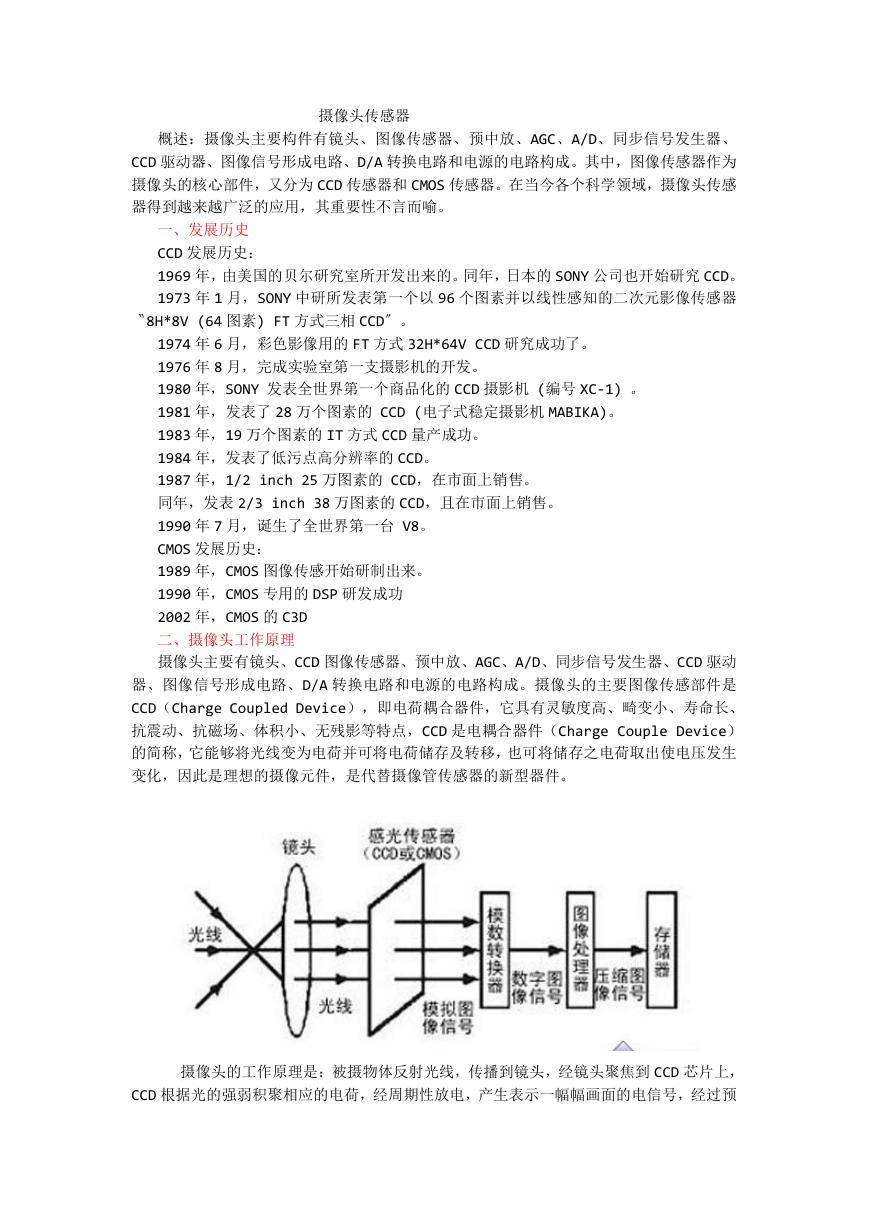 摄像头工作原理.doc
 VL53L0X简要说明(En.FLVL53L00216).pdf
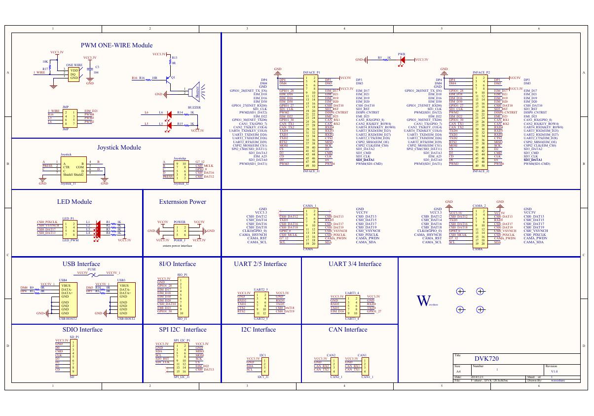 原理图(DVK720-Schematic).pdf
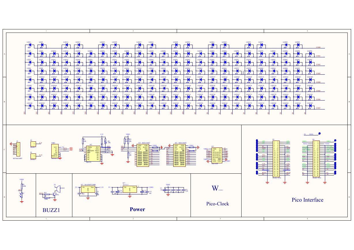 原理图(Pico-Clock-Green-Schdoc).pdf
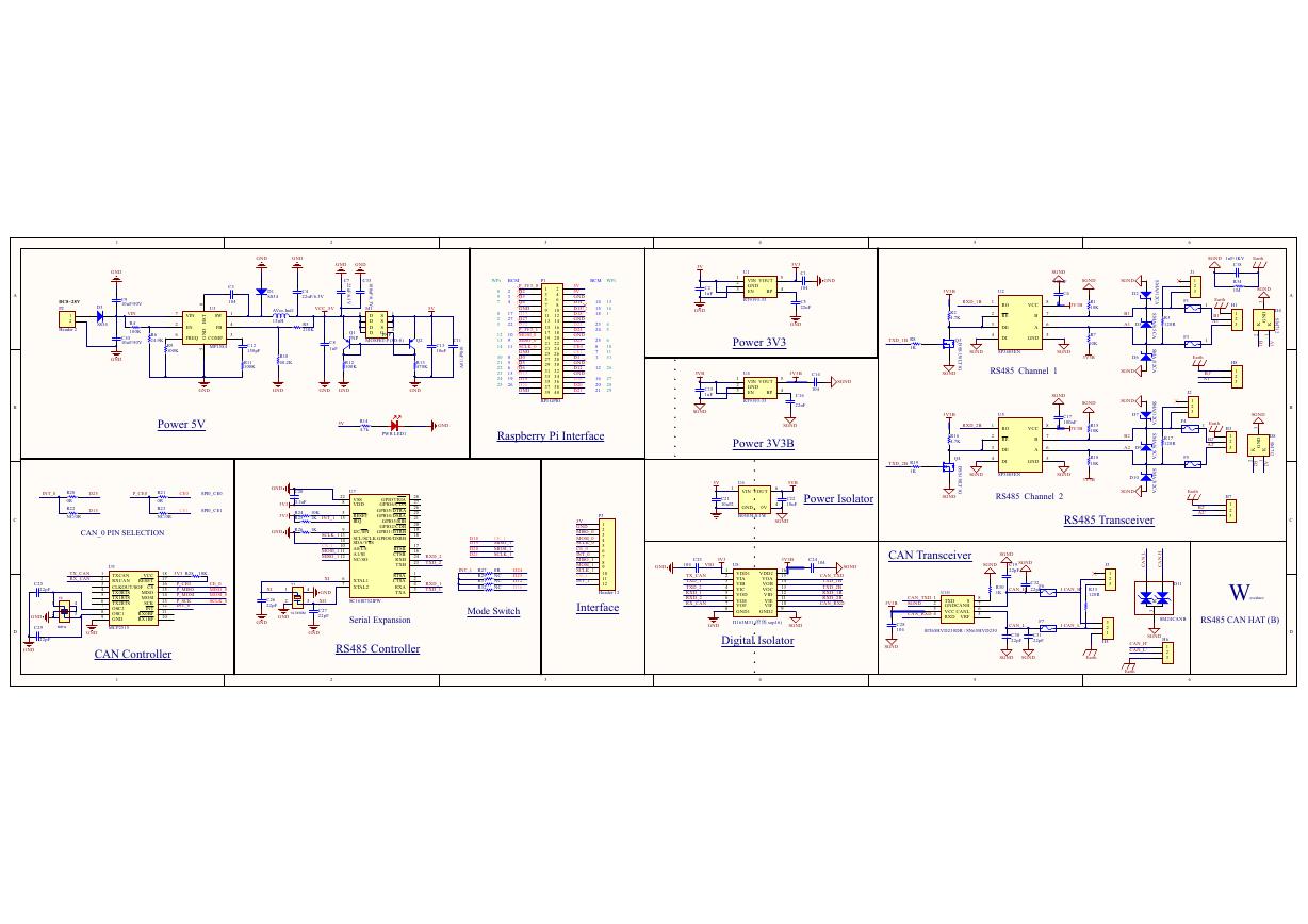 原理图(RS485-CAN-HAT-B-schematic).pdf
 File:SIM7500_SIM7600_SIM7800 Series_SSL_Application Note_V2.00.pdf
 ADS1263(Ads1262).pdf
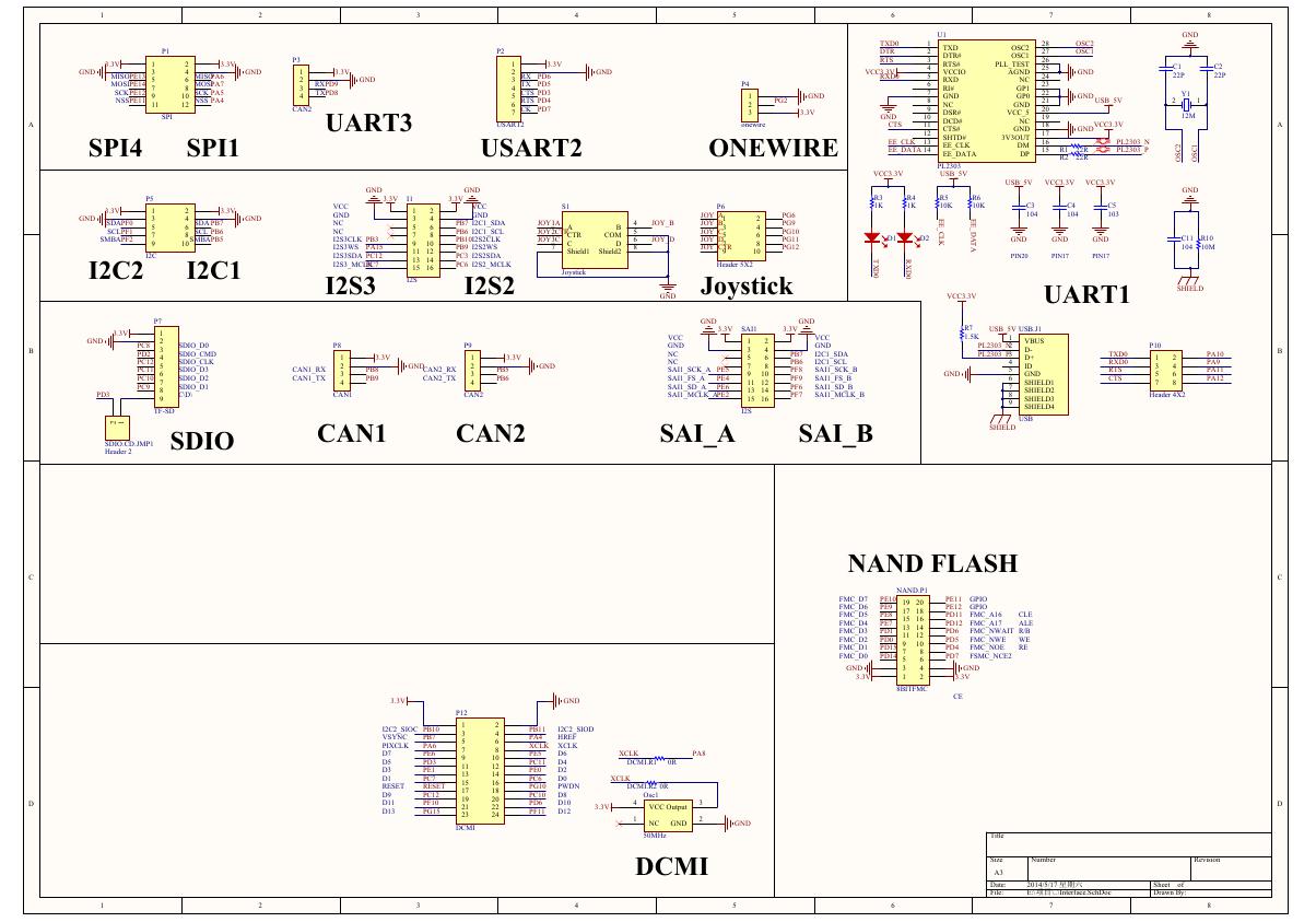 原理图(Open429Z-D-Schematic).pdf
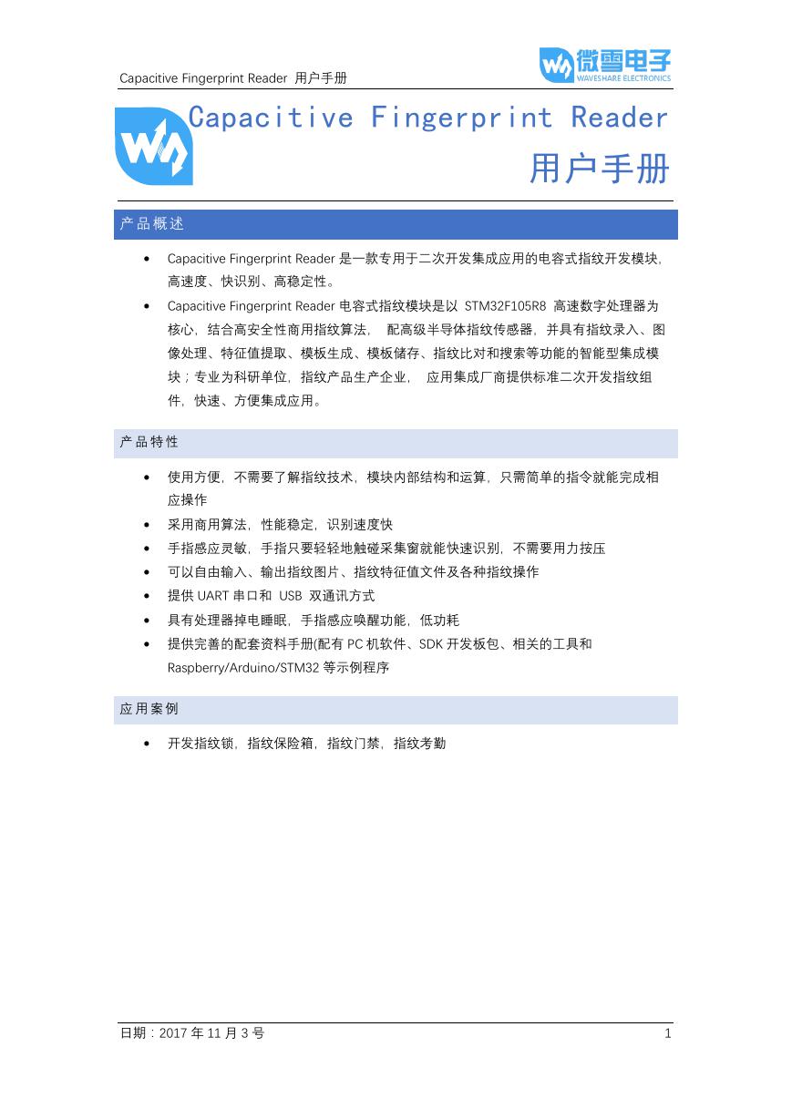 用户手册(Capacitive_Fingerprint_Reader_User_Manual_CN).pdf
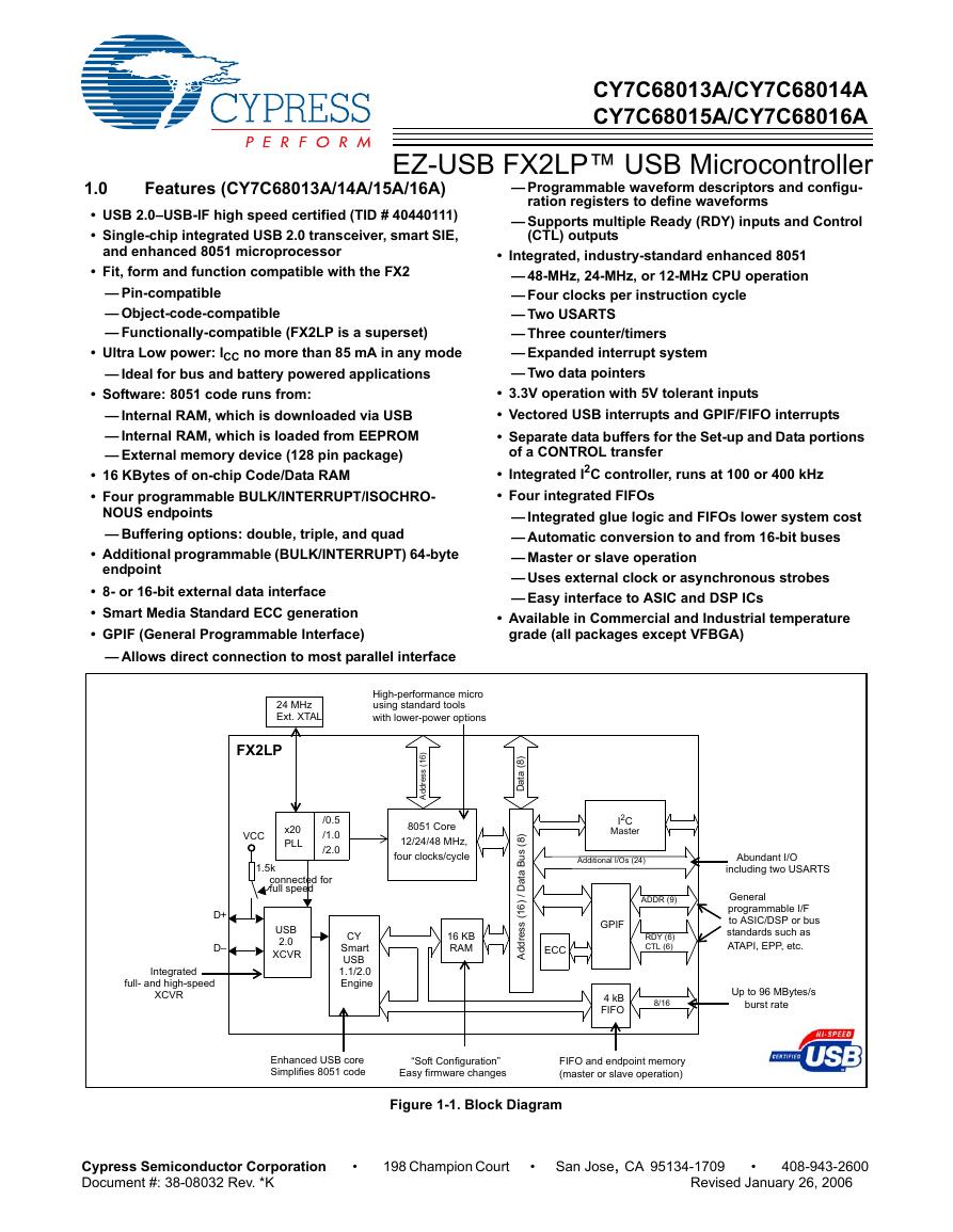 CY7C68013A(英文版)(CY7C68013A).pdf
 TechnicalReference_Dem.pdf