SN74LVC1G126 Single Bus Buffer Gate With 3-State Output
SN74LVC1G126
SCES224R –APRIL 1999–REVISED JANUARY 2015
1 Features
1• Available in the Texas Instruments
NanoFree™ Package
Inputs Accept Voltages to 5.5 V
• Supports 5-V VCC Operation
•
• Provides Down Translation to VCC
• Max tpd of 3.7 ns at 3.3 V
•
•
•
Low Power Consumption, 10-μA Max ICC
±24-mA Output Drive at 3.3 V
Ioff Supports Live Insertion, Partial-Power-Down
Mode, and Back Drive Protection
Latch-Up Performance Exceeds 100 mA
Per JESD 78, Class II
•
• ESD Protection Exceeds JESD 22
– 2000-V Human-Body Model
– 200-V Machine Model
– 1000-V Charged-Device Model
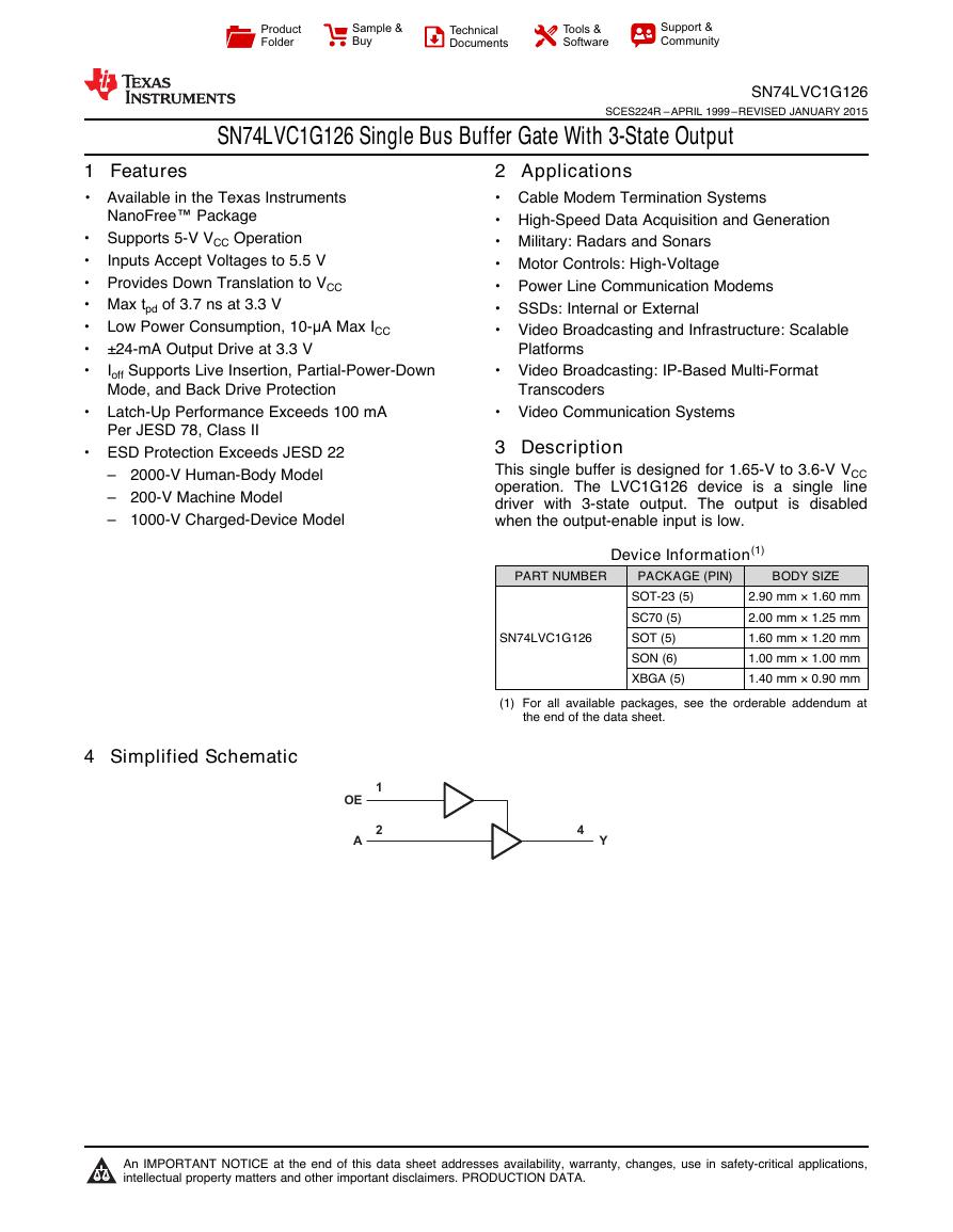
4 Simplified Schematic
2 Applications
• Cable Modem Termination Systems
• High-Speed Data Acquisition and Generation
• Military: Radars and Sonars
• Motor Controls: High-Voltage
• Power Line Communication Modems
• SSDs: Internal or External
• Video Broadcasting and Infrastructure: Scalable
Platforms
• Video Broadcasting: IP-Based Multi-Format
Transcoders
• Video Communication Systems
3 Description
This single buffer is designed for 1.65-V to 3.6-V VCC
operation. The LVC1G126 device is a single line
driver with 3-state output. The output
is disabled
when the output-enable input is low.
Device Information(1)
BODY SIZE
the end of the data sheet.
SN74LVC1G126
PART NUMBER
PACKAGE (PIN)
SOT-23 (5)
SC70 (5)
SOT (5)
SON (6)
XBGA (5)
2.90 mm × 1.60 mm
2.00 mm × 1.25 mm
1.60 mm × 1.20 mm
1.00 mm × 1.00 mm
1.40 mm × 0.90 mm
(1) For all available packages, see the orderable addendum at
1
An IMPORTANT NOTICE at the end of this data sheet addresses availability, warranty, changes, use in safety-critical applications,
intellectual property matters and other important disclaimers. PRODUCTION DATA.
AYOE124ProductFolderSample &BuyTechnicalDocumentsTools &SoftwareSupport &Community�
SN74LVC1G126
SCES224R –APRIL 1999–REVISED JANUARY 2015
www.ti.com
Table of Contents
1
Features.................................................................. 1
2 Applications ........................................................... 1
3 Description ............................................................. 1
4 Simplified Schematic............................................. 1
5 Revision History..................................................... 2
6 Pin Configuration and Functions ......................... 3
7 Specifications......................................................... 4
7.1 Absolute Maximum Ratings ..................................... 4
7.2 ESD Ratings.............................................................. 4
7.3 Recommended Operating Conditions ...................... 5
7.4 Thermal Information.................................................. 5
7.5 Electrical Characteristics........................................... 6
7.6 Switching Characteristics, CL = 15 pF ...................... 6
7.7 Switching Characteristics, –40°C to 85°C................. 6
7.8 Switching Characteristics, –40°C to 125°C............... 7
7.9 Operating Characteristics ........................................ 7
7.10 Typical Characteristics............................................ 7
8 Parameter Measurement Information .................. 8
5 Revision History
9 Detailed Description ............................................ 10
9.1 Overview ................................................................. 10
9.2 Functional Block Diagram ....................................... 10
9.3 Feature Description................................................. 10
9.4 Device Functional Modes........................................ 10
10 Application and Implementation........................ 11
10.1 Application Information.......................................... 11
10.2 Typical Application ............................................... 11
11 Power Supply Recommendations ..................... 12
12 Layout................................................................... 12
12.1 Layout Guidelines ................................................. 12
12.2 Layout Example .................................................... 12
13 Device and Documentation Support ................. 13
13.1 Trademarks ........................................................... 13
13.2 Electrostatic Discharge Caution............................ 13
13.3 Glossary ................................................................ 13
14 Mechanical, Packaging, and Orderable
Information ........................................................... 13
Changes from Revision Q (December 2013) to Revision R
Page
• Added Applications, Device Information table, Handling Ratings table, Feature Description section, Device
Functional Modes, Application and Implementation section, Power Supply Recommendations section, Layout
section, Device and Documentation Support section, and Mechanical, Packaging, and Orderable Information section...... 1
Changes from Revision P (November 2012) to Revision Q
Page
• Updated document to new TI data sheet format. ................................................................................................................... 1
• Changed MAX operating temperature to 125°C in Recommended Operating Conditions table. ......................................... 5
• Added ESD warning. ............................................................................................................................................................ 13
Changes from Revision O (March 2011) to Revision P
Page
• Removed Ordering Information table. .................................................................................................................................... 1
Changes from Revision N (February 2007) to Revision O
Page
• Added DSF package option to the data sheet. ...................................................................................................................... 3
2
Submit Documentation Feedback
Copyright © 1999–2015, Texas Instruments Incorporated
Product Folder Links: SN74LVC1G126
�
www.ti.com
6 Pin Configuration and Functions
SN74LVC1G126
SCES224R –APRIL 1999–REVISED JANUARY 2015
See mechanical drawings for dimensions.
Pin Functions
PIN
SN74LVC1G126
NAME
DBV, DCK,
DRL, YZP
DRY, DSF
A
GND
NC
OE
VCC
Y
2
3
—
1
5
4
2
3
5
1
6
4
TYPE
I
—
—
I
—
O
A Input
Ground Pin
Do not connect
OE Enable/Input
Power Pin
Y Output
DESCRIPTION
Copyright © 1999–2015, Texas Instruments Incorporated
Submit Documentation Feedback
3
Product Folder Links: SN74LVC1G126
DBV PACKAGE(TOPVIEW)2534Y1AGNDOEVCCDCK PACKAGE(TOPVIEW)342Y1GNDAOE5VCCDRLPACKAGE(TOPVIEW)2A1OE34GNDY5VCCDRYPACKAGE(TOPVIEW)AN.C.OE65423GNDYVCC1YZPPACKAGE(BOTTOM VIEW)2A1OEGND43Y5VCCA1B1C1A2C2OEGNDDSF PACKAGE(TOPVIEW)AVCCYN.C.654231�
SN74LVC1G126
SCES224R –APRIL 1999–REVISED JANUARY 2015
7 Specifications
7.1 Absolute Maximum Ratings
over operating free-air temperature range (unless otherwise noted)(1)
VCC
VI
VO
VO
IIK
IOK
IO
Supply voltage range
Input voltage range(2)
Voltage range applied to any output in the high-impedance or power-off state(2)
Voltage range applied to any output in the high or low state(2)(3)
Input clamp current
Output clamp current
Continuous output current
Continuous current through VCC or GND
Storage temperature range
VI < 0
VO < 0
www.ti.com
UNIT
MAX
MIN
6.5
–0.5
6.5
–0.5
–0.5
6.5
–0.5 VCC + 0.5
–50
–50
±50
±100
150
–65
V
V
V
V
mA
mA
mA
mA
°C
Tstg
(1) Stresses beyond those listed under Absolute Maximum Ratings may cause permanent damage to the device. These are stress ratings
only, and functional operation of the device at these or any other conditions beyond those indicated under Recommended Operating
Conditions is not implied. Exposure to absolute-maximum-rated conditions for extended periods may affect device reliability.
(2) The input negative-voltage and output voltage ratings may be exceeded if the input and output current ratings are observed.
(3) The value of VCC is provided in the Recommended Operating Conditions table.
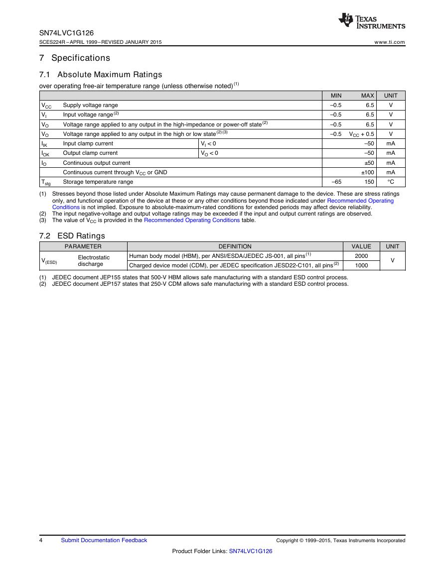
7.2 ESD Ratings
PARAMETER
DEFINITION
V(ESD)
Electrostatic
discharge
Human body model (HBM), per ANSI/ESDA/JEDEC JS-001, all pins(1)
Charged device model (CDM), per JEDEC specification JESD22-C101, all pins(2)
(1)
(2)
JEDEC document JEP155 states that 500-V HBM allows safe manufacturing with a standard ESD control process.
JEDEC document JEP157 states that 250-V CDM allows safe manufacturing with a standard ESD control process.
VALUE
2000
1000
UNIT
V
4
Submit Documentation Feedback
Copyright © 1999–2015, Texas Instruments Incorporated
Product Folder Links: SN74LVC1G126
�
www.ti.com
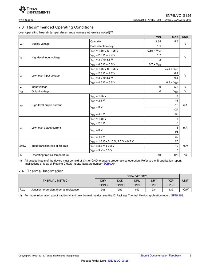
7.3 Recommended Operating Conditions
over operating free-air temperature range (unless otherwise noted)(1)
SN74LVC1G126
SCES224R –APRIL 1999–REVISED JANUARY 2015
MAX UNIT
5.5
V
V
V
V
V
mA
mA
ns/V
°C
0.35 × VCC
0.7
0.8
0.3 × VCC
5.5
VCC
–4
–8
–16
–24
–32
4
8
16
24
32
20
10
5
125
VCC
Supply voltage
VIH
High-level input voltage
VIL
VI
VO
IOH
Low-level input voltage
Input voltage
Output voltage
High-level output current
IOL
Low-level output current
Δt/Δv
Input transition rise or fall rate
MIN
1.65
1.5
0.65 × VCC
1.7
2
0.7 × VCC
0
0
Operating
Data retention only
VCC = 1.65 V to 1.95 V
VCC = 2.3 V to 2.7 V
VCC = 3 V to 3.6 V
VCC = 4.5 V to 5.5 V
VCC = 1.65 V to 1.95 V
VCC = 2.3 V to 2.7 V
VCC = 3 V to 3.6 V
VCC = 4.5 V to 5.5 V
VCC = 1.65 V
VCC = 2.3 V
VCC = 3 V
VCC = 4.5 V
VCC = 1.65 V
VCC = 2.3 V
VCC = 3 V
VCC = 4.5 V
VCC = 1.8 V ± 0.15 V, 2.5 V ± 0.2 V
VCC = 3.3 V ± 0.3 V
VCC = 5 V ± 0.5 V
Operating free-air temperature
TA
(1) All unused inputs of the device must be held at VCC or GND to ensure proper device operation. Refer to the TI application report,
–40
Implications of Slow or Floating CMOS Inputs, literature number SCBA004.
7.4 Thermal Information
THERMAL METRIC(1)
SN74LVC1G126
DBV
5 PINS
DCK
5 PINS
DRL
5 PINS
DRY
6 PINS
YZP
5 PINS
UNIT
Junction-to-ambient thermal resistance
RθJA
(1) For more information about traditional and new thermal metrics, see the IC Package Thermal Metrics application report, SPRA953.
206
252
142
234
132
°C/W
Copyright © 1999–2015, Texas Instruments Incorporated
Submit Documentation Feedback
5
Product Folder Links: SN74LVC1G126
�
1.65 V to 5.5 V
VCC – 0.1
1.2
1.9
2.4
2.3
3.8
1.65 V
2.3 V
3 V
4.5 V
1.65 V to 5.5 V
1.65 V
2.3 V
3 V
4.5 V
0 to 5.5 V
0
3.6 V
1.65 V to 5.5 V
3 V to 5.5 V
0.1
0.45
0.3
0.4
0.55
0.55
±5
±10
10
10
500
–40°C to 125°C
TYP(1)
MAX
MIN
VCC –
0.1
1.2
1.9
2.4
2.3
3.8
0.1
0.45
0.3
0.4
0.55
0.55
±5
±10
10
10
500
4
UNIT
V
V
μA
μA
μA
μA
μA
pF
UNIT
ns
SN74LVC1G126
SCES224R –APRIL 1999–REVISED JANUARY 2015
7.5 Electrical Characteristics
over recommended operating free-air temperature range (unless otherwise noted)
PARAMETER
TEST CONDITIONS
VCC
–40°C to 85°C
TYP(1)
MIN
MAX
www.ti.com
IOH = –100 μA
IOH = –4 mA
IOH = –8 mA
IOH = –16 mA
IOH = –24 mA
IOH = –32 mA
IOL = 100 μA
IOL = 4 mA
IOL = 8 mA
IOL = 16 mA
IOL = 24 mA
IOL = 32 mA
A or OE
inputs
VI = 5.5 V or GND
VOH
VOL
II
Ioff
IOZ
ICC
ΔICC
VI or VO = 5.5 V
VO = 0 to 5.5 V
VI = 5.5 V or GND
One input at VCC – 0.6 V,
Other inputs at VCC or GND
VI = VCC or GND
IO = 0
Ci
(1) All typical values are at VCC = 3.3 V, TA = 25°C.
7.6 Switching Characteristics, CL = 15 pF
over recommended operating free-air temperature range, CL = 15 pF (unless otherwise noted) (see Figure 3)
3.3 V
4
PARAMETER
tpd
FROM
(INPUT)
A
TO
(OUTPUT)
Y
VCC = 1.8 V
± 0.15 V
MIN MAX
1.7
6.9
VCC = 2.5 V
± 0.2 V
MIN
0.6
VCC = 3.3 V
± 0.3 V
VCC = 5 V
± 0.5 V
MAX
4.6
MIN
0.6
MAX
3.7
MIN
0.5
MAX
3.4
–40°C to 85°C
7.7 Switching Characteristics, –40°C to 85°C
over recommended operating free-air temperature range, CL = 30 pF or 50 pF (unless otherwise noted) (see Figure 4)
–40°C to 85°C
PARAMETER
tpd
ten
tdis
FROM
(INPUT)
A
OE
OE
TO
(OUTPUT)
Y
Y
Y
VCC = 1.8 V
± 0.15 V
MIN MAX
2.6
8
9.4
2.8
1.6
9.8
VCC = 2.5 V
± 0.2 V
MIN
1.1
1.3
1
VCC = 3.3 V
± 0.3 V
VCC = 5 V
± 0.5 V
UNIT
MAX
5.5
6.6
5.5
MIN
1
1.2
1
MAX
4.5
5.3
5.5
MIN
1
1
1
MAX
4
5
4.2
ns
ns
ns
6
Submit Documentation Feedback
Copyright © 1999–2015, Texas Instruments Incorporated
Product Folder Links: SN74LVC1G126
�
www.ti.com
SN74LVC1G126
SCES224R –APRIL 1999–REVISED JANUARY 2015
7.8 Switching Characteristics, –40°C to 125°C
over recommended operating free-air temperature range, CL = 30 pF or 50 pF (unless otherwise noted) (see Figure 4)
–40°C to 125°C
PARAMETER
tpd
ten
tdis
FROM
(INPUT)
A
OE
OE
TO
(OUTPUT)
Y
Y
Y
VCC = 1.8 V
± 0.15 V
MIN MAX
9
2.6
9.6
2.8
1.6
10
VCC = 2.5 V
± 0.2 V
MIN
1.1
1.3
1
VCC = 3.3 V
± 0.3 V
VCC = 5 V
± 0.5 V
UNIT
MAX
5.7
6.8
5.7
MIN
1
1.2
1
MAX
4.7
5.5
5.7
MIN
1
1
1
MAX
4.2
5.2
4.4
ns
ns
ns
7.9 Operating Characteristics
TA = 25°C
PARAMETER
Cpd
Power dissipation
capacitance
Outputs enabled
Outputs disabled
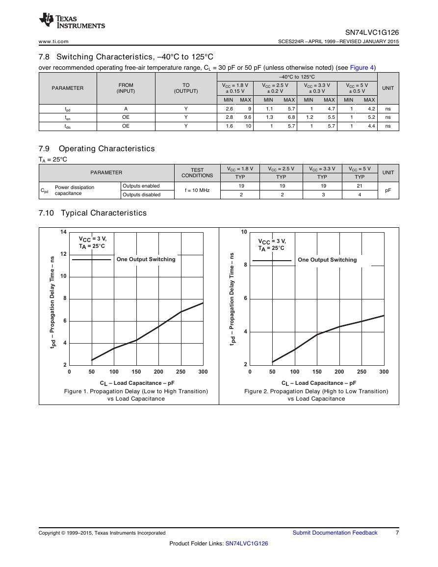
7.10 Typical Characteristics
TEST
CONDITIONS
f = 10 MHz
VCC = 1.8 V
VCC = 2.5 V
VCC = 3.3 V
VCC = 5 V
TYP
19
2
TYP
19
2
TYP
19
3
TYP
21
4
UNIT
pF
Figure 1. Propagation Delay (Low to High Transition)
vs Load Capacitance
Figure 2. Propagation Delay (High to Low Transition)
vs Load Capacitance
Copyright © 1999–2015, Texas Instruments Incorporated
Submit Documentation Feedback
7
Product Folder Links: SN74LVC1G126
2468101214050100150200250300CL–LoadCapacitance–pFVCC=3V,TA=25°COneOutputSwitchingt–PropagationDelayTime–nspd246810050100150200250300CL–LoadCapacitance–pFt–PropagationDelayTime–nspdVCC=3V,TA=25°COneOutputSwitching�
SN74LVC1G126
SCES224R –APRIL 1999–REVISED JANUARY 2015
8 Parameter Measurement Information
www.ti.com
Figure 3. Load Circuit and Voltage Waveforms
8
Submit Documentation Feedback
Copyright © 1999–2015, Texas Instruments Incorporated
Product Folder Links: SN74LVC1G126
VMthtsuFrom OutputUnder TestCL(see NoteA)LOAD CIRCUITS1VLOADOpenGNDRRLLData InputTiming InputVI0 VVI0 V0 VtInputwVOLTAGEWAVEFORMSSETUPAND HOLD TIMESVOLTAGEWAVEFORMSPROPAGATIONDELAYTIMESINVERTINGAND NONINVERTING OUTPUTSVOLTAGEWAVEFORMSPULSEDURATIONtPLHtPHLtPHLtPLHVOHVOHVOLVOLVI0 VInputOutputWaveform 1S1 at VLOAD(see Note B)OutputWaveform 2S1 at GND(see Note B)VOLVOHtPZLtPZHtPLZtPHZVLOAD/20 VVOL+V∆VOH−V∆≈0 VVIVOLTAGEWAVEFORMSENABLEAND DISABLE TIMESLOW-ANDHIGH-LEVELENABLINGOutputOutputtPLH/tPHLtPLZ/tPZLtPHZ/tPZHOpenVLOADGNDTESTS1NOTES:A.CLincludes probe and jig capacitance.B.Waveform1isforanoutputwithinternalconditionssuchthattheoutputislow,exceptwhendisabledbytheoutputcontrol.Waveform2is for an output with internal conditions such that the output is high, except when disabled by the output control.C.All input pulses are supplied by generators having the following characteristics: PRR≤10 MHz, ZO= 50Ω.D.The outputs are measured one at a time, with one transition per measurement.E.tPLZand tPHZare the same as tdis.F.tPZLand tPZHare the same as ten.G.tPLHand tPHLare the same as tpd.H.All parameters and waveforms are not applicable to all devices.OutputControlVVVVVVVVVVVVVMMMMMMMMMMMMIVMVM1.8 V±0.15 V2.5 V±0.2 V3.3 V±0.3 V5V±0.5 V1 MΩ1 MΩ1 MΩ1 MΩVCCRL2×VCC2×VCC6 V2×VCCVLOADCL15 pF15 pF15 pF15 pF0.15 V0.15 V0.3 V0.3 VVV∆CCVCC3 VVCCVVICC/2VCC/21.5 VVCC/2VMt/trf≤2ns≤2ns≤2.5 ns≤2.5 nsINPUTS�





 V2版本原理图(Capacitive-Fingerprint-Reader-Schematic_V2).pdf
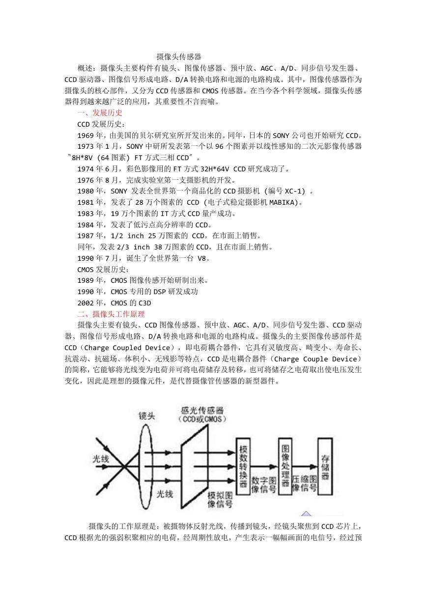 摄像头工作原理.doc
 VL53L0X简要说明(En.FLVL53L00216).pdf
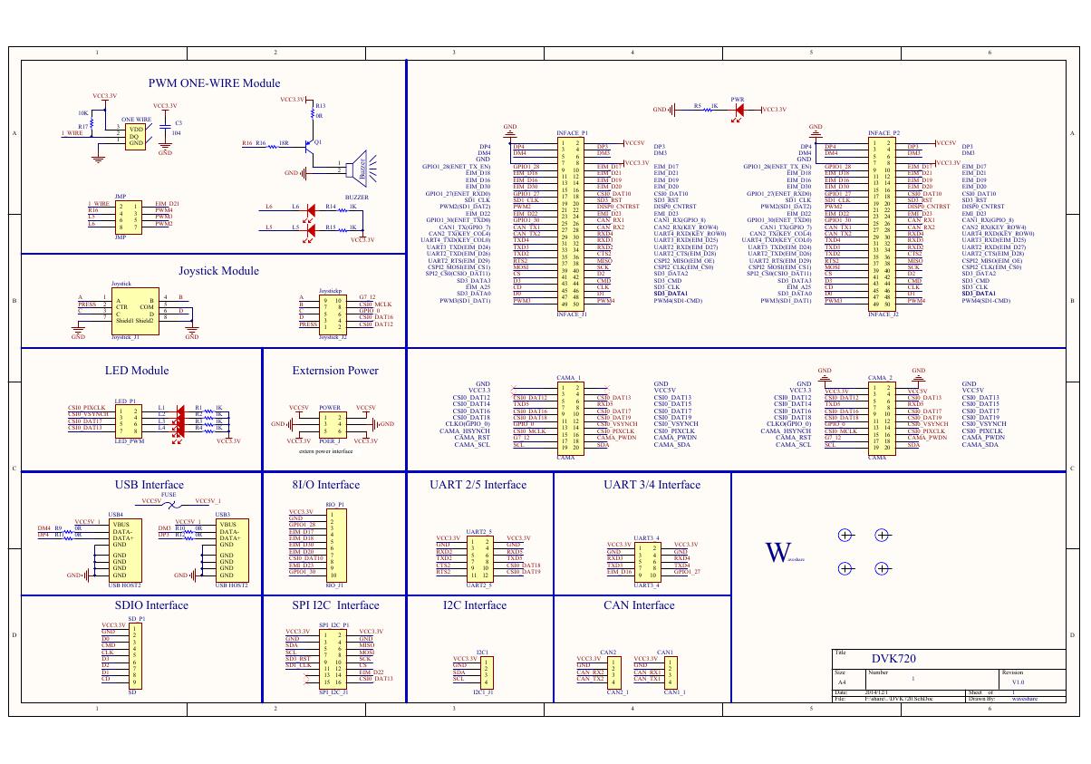 原理图(DVK720-Schematic).pdf
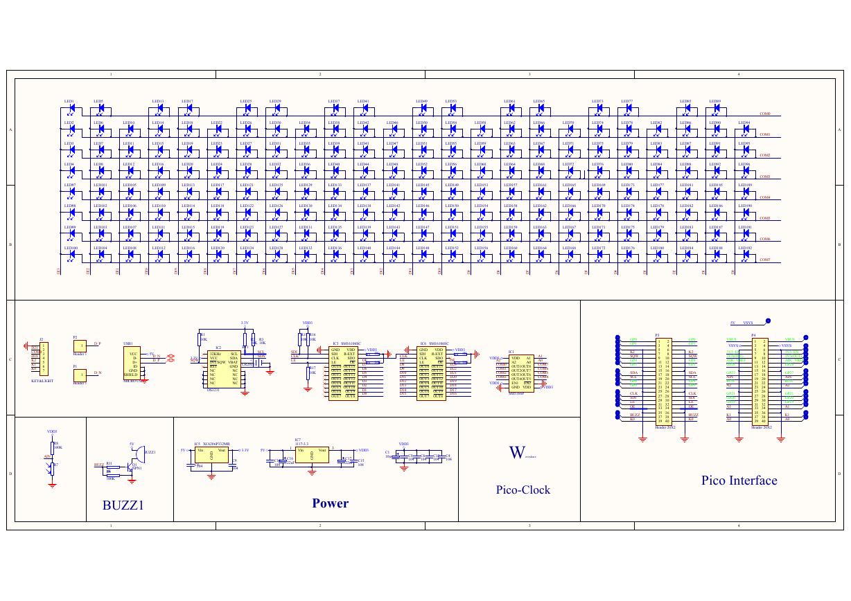 原理图(Pico-Clock-Green-Schdoc).pdf
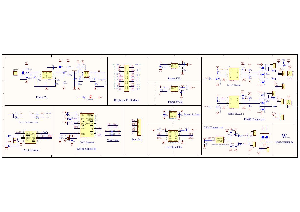 原理图(RS485-CAN-HAT-B-schematic).pdf
 File:SIM7500_SIM7600_SIM7800 Series_SSL_Application Note_V2.00.pdf
 ADS1263(Ads1262).pdf
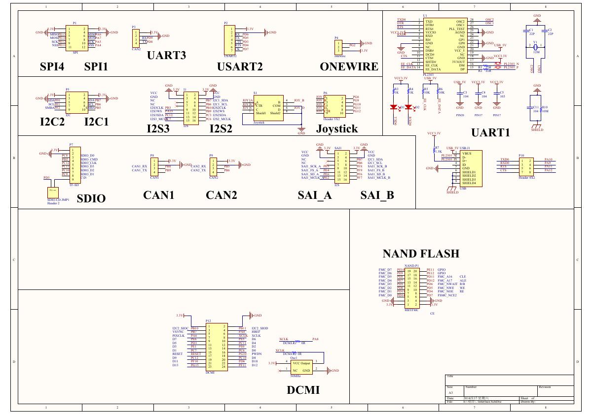 原理图(Open429Z-D-Schematic).pdf
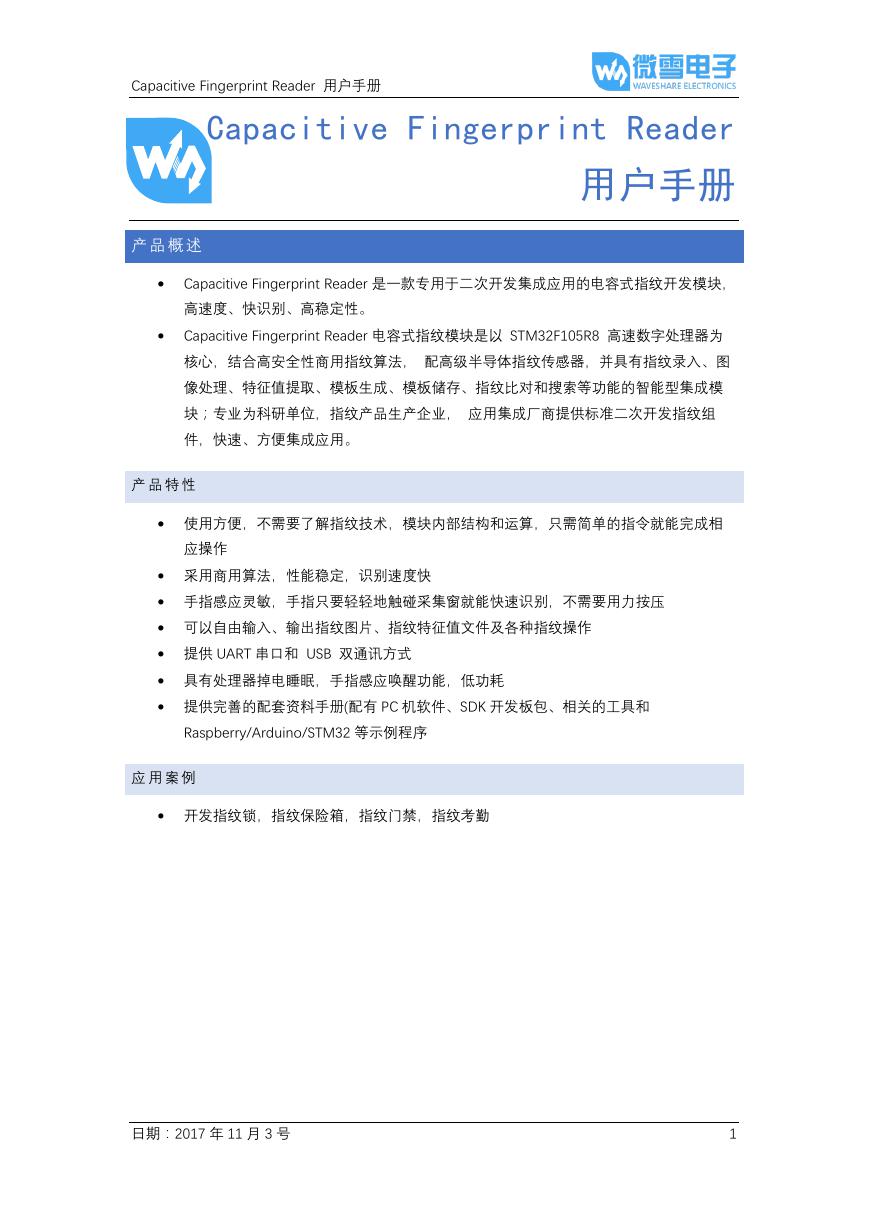 用户手册(Capacitive_Fingerprint_Reader_User_Manual_CN).pdf
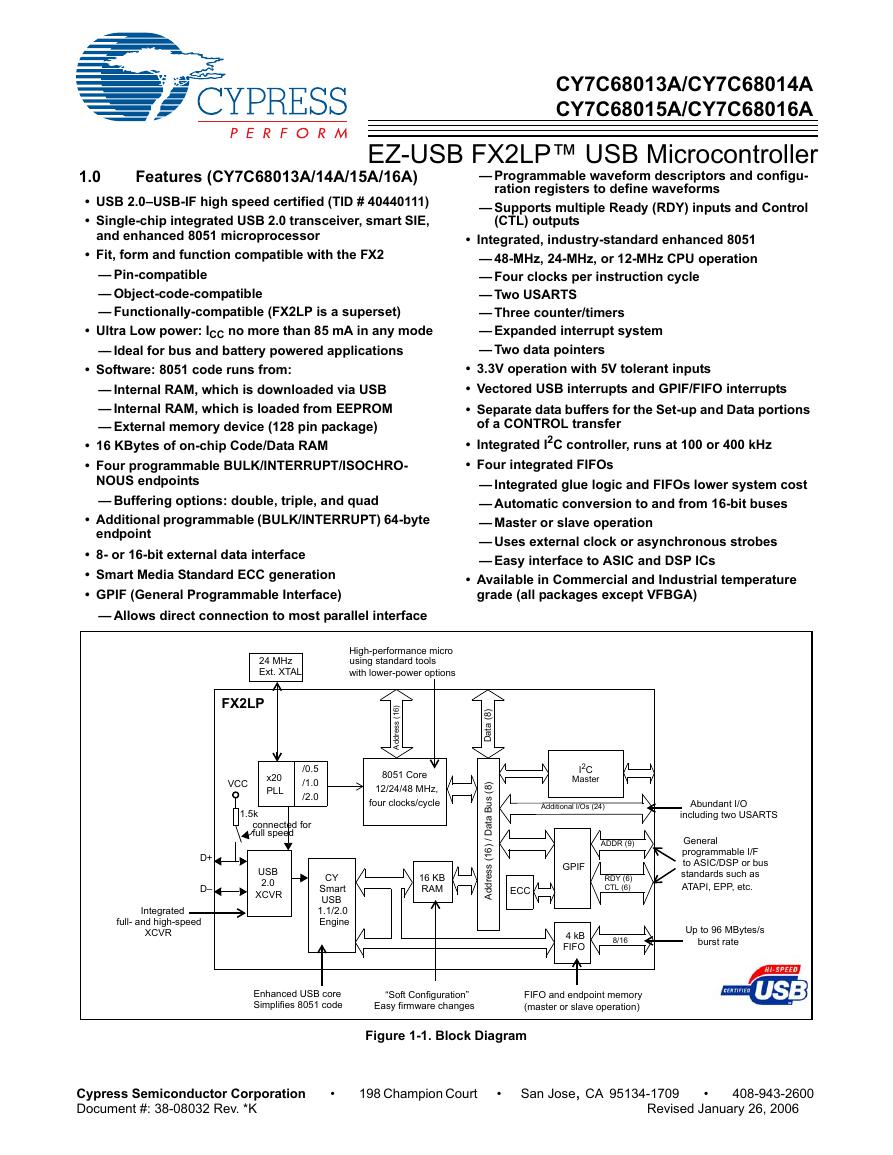 CY7C68013A(英文版)(CY7C68013A).pdf
 TechnicalReference_Dem.pdf