###E###
###E###
###E###
###E###
MC54/74HC595A
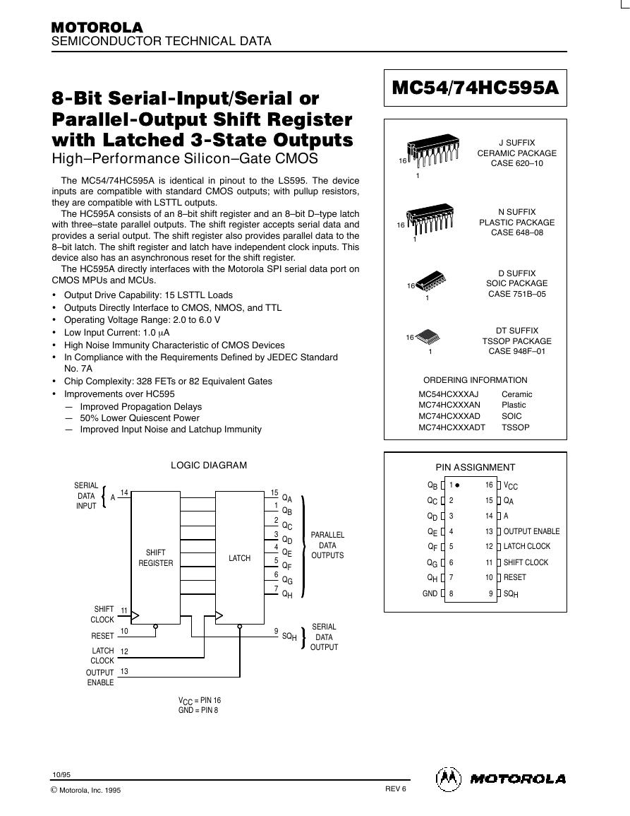
PIN DESCRIPTIONS
INPUTS
A (Pin 14)
Serial Data Input. The data on this pin is shifted into the
8–bit serial shift register.
CONTROL INPUTS
Shift Clock (Pin 11)
Shift Register Clock Input. A low– to–high transition on this
input causes the data at the Serial Input pin to be shifted into
the 8–bit shift register.
Reset (Pin 10)
Latch Clock (Pin 12)
Storage Latch Clock Input. A low–to–high transition on this
input latches the shift register data.
Output Enable (Pin 13)
Active–low Output Enable. A low on this input allows the
data from the latches to be presented at the outputs. A high
on this input forces the outputs (QA–QH) into the high–
impedance state. The serial output is not affected by this
control unit.
OUTPUTS
QA – QH (Pins 15, 1, 2, 3, 4, 5, 6, 7)
Noninverted, 3–state, latch outputs.
SQH (Pin 9)
Active–low, Asynchronous, Shift Register Reset Input. A
low on this pin resets the shift register portion of this device
only. The 8–bit latch is not affected.
Noninverted, Serial Data Output. This is the output of the
eighth stage of the 8–bit shift register. This output does not
have three–state capability.
High–Speed CMOS Logic Data
DL129 — Rev 6
5
MOTOROLA
�
MC54/74HC595A
tr
tf
SHIFT
CLOCK
OUTPUT
SQH
90%
50%
10%
90%
50%
10%
tw
1/fmax
tPLH
tPHL
tTLH
tTHL
Figure 1.
LATCH
CLOCK
50%
QA–QH
OUTPUTS
90%
50%
10%
SERIAL
INPUT A
LATCH
CLOCK
tPLH
tPHL
tTLH
tTHL
Figure 3.
50%
tsu
VALID
th
50%
Figure 5.
SWITCHING WAVEFORMS
VCC
GND
VCC
GND
VCC
GND
VCC
GND
RESET
OUTPUT
SQH
SHIFT
CLOCK
tw
50%
tPHL
50%
trec
50%
Figure 2.
OUTPUT
ENABLE
50%
tPZL
tPLZ
OUTPUT Q
50%
tPZH
tPHZ
OUTPUT Q
50%
SHIFT
CLOCK
LATCH
CLOCK
Figure 4.
50%
tsu
50%
tw
Figure 6.
VCC
GND
VCC
GND
VCC
GND
10%
90%
HIGH
IMPEDANCE
VOL
VOH
HIGH
IMPEDANCE
VCC
GND
VCC
GND
TEST CIRCUITS
TEST POINT
OUTPUT
CL*
DEVICE
UNDER
TEST
TEST POINT
OUTPUT
1 kW
CL*
DEVICE
UNDER
TEST
CONNECT TO VCC WHEN
TESTING tPLZ AND tPZL.
CONNECT TO GND WHEN
TESTING tPHZ AND tPZH.
* Includes all probe and jig capacitance
* Includes all probe and jig capacitance
Figure 7.
Figure 8.
MOTOROLA
6
High–Speed CMOS Logic Data
DL129 — Rev 6
�
13
12
14
OUTPUT
ENABLE
LATCH
CLOCK
SERIAL
DATA
INPUT A
SHIFT
CLOCK
RESET
11
10
EXPANDED LOGIC DIAGRAM
MC54/74HC595A
Q
Q
Q
Q
Q
Q
Q
Q
SRA
SRB
SRC
SRD
SRE
SRF
SRG
SRH
D
R
D
R
D
R
D
R
D
R
D
R
D
R
D
R
D
Q
LRA
D
Q
LRB
D
Q
LRC
D
Q
LRD
D
Q
LRE
D
Q
LRF
D
Q
LRG
D
Q
LRH
15
QA
1
2
3
4
5
6
7
9
PARALLEL
DATA
OUTPUTS
QB
QC
QD
QE
QF
QG
QH
SERIAL
DATA
OUTPUT SQH
High–Speed CMOS Logic Data
DL129 — Rev 6
7
MOTOROLA
�
MC54/74HC595A
TIMING DIAGRAM
SHIFT
CLOCK
SERIAL DATA
INPUT A
RESET
LATCH
CLOCK
OUTPUT
ENABLE
QA
QB
QC
QD
QE
QF
QG
QH
SERIAL DATA
OUTPUT SQH
NOTE:
implies that the output is in a high–impedance
state.
MOTOROLA
8
High–Speed CMOS Logic Data
DL129 — Rev 6
�


 V2版本原理图(Capacitive-Fingerprint-Reader-Schematic_V2).pdf
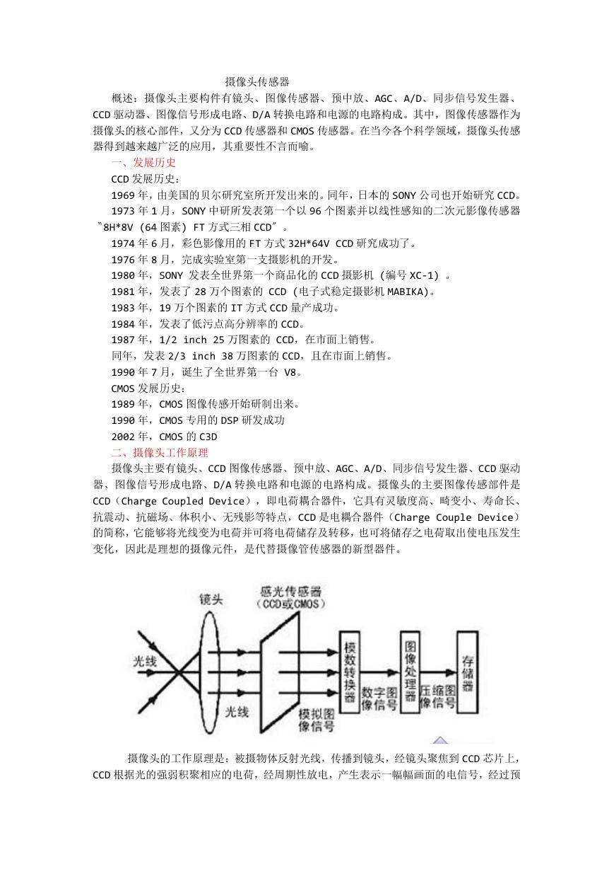 摄像头工作原理.doc
 VL53L0X简要说明(En.FLVL53L00216).pdf
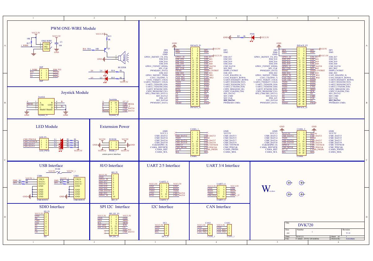 原理图(DVK720-Schematic).pdf
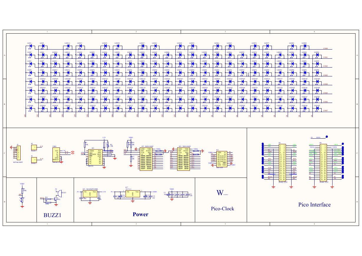 原理图(Pico-Clock-Green-Schdoc).pdf
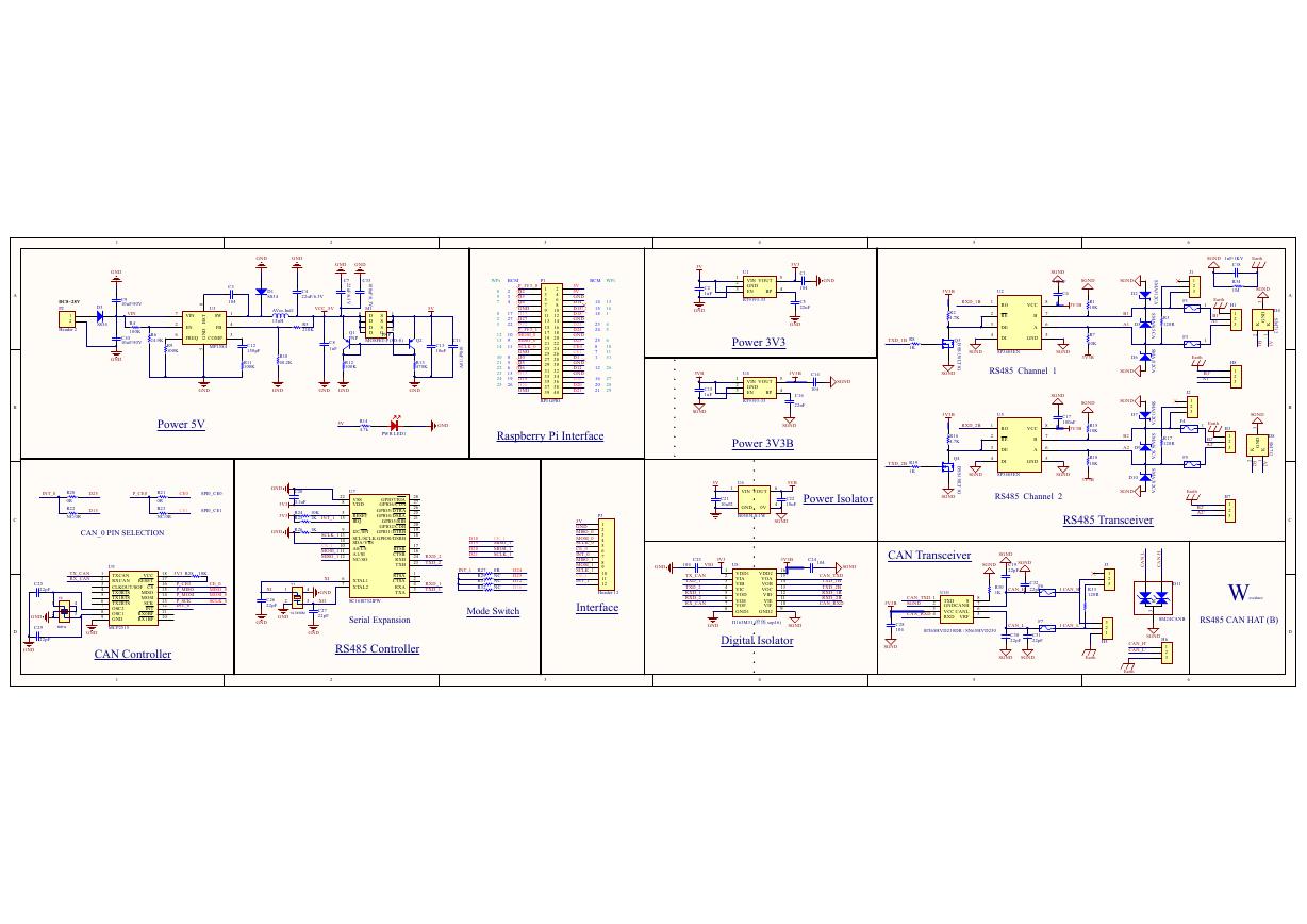 原理图(RS485-CAN-HAT-B-schematic).pdf
 File:SIM7500_SIM7600_SIM7800 Series_SSL_Application Note_V2.00.pdf
 ADS1263(Ads1262).pdf
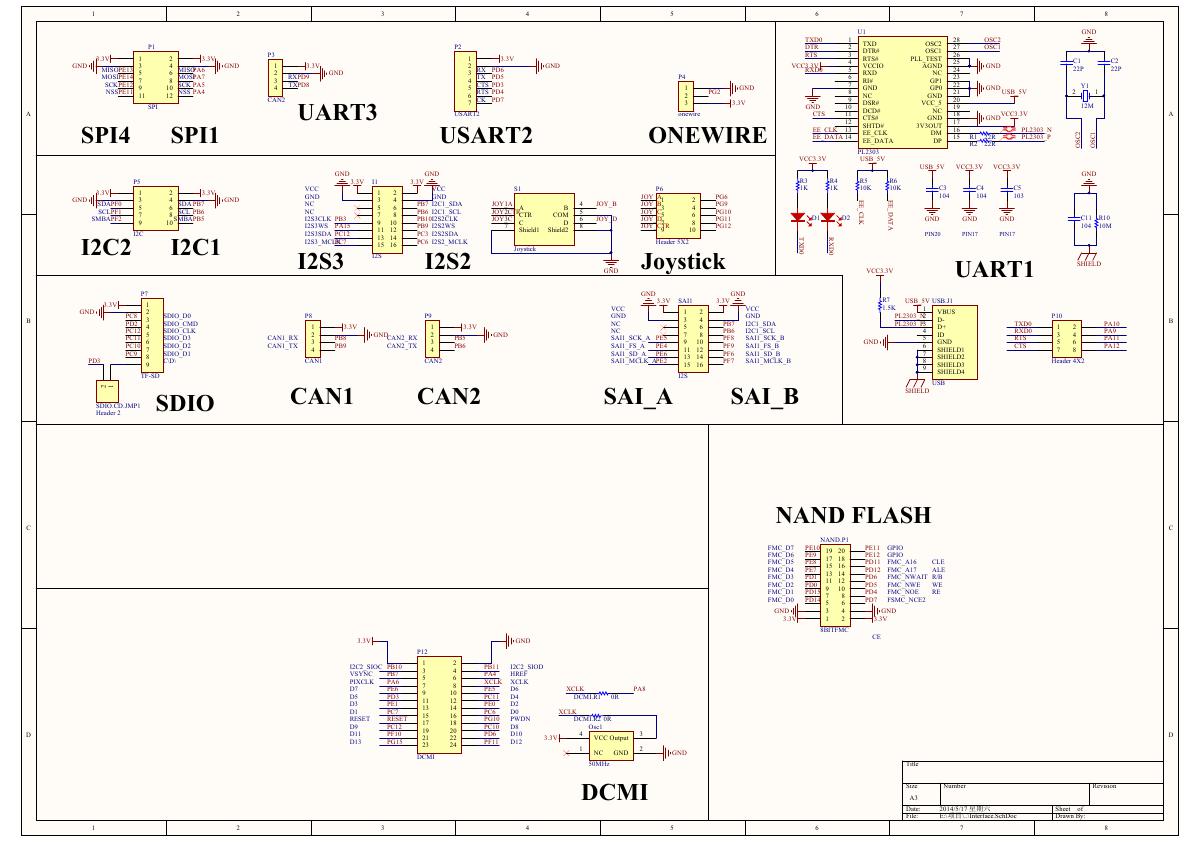 原理图(Open429Z-D-Schematic).pdf
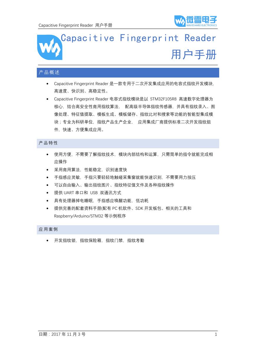 用户手册(Capacitive_Fingerprint_Reader_User_Manual_CN).pdf
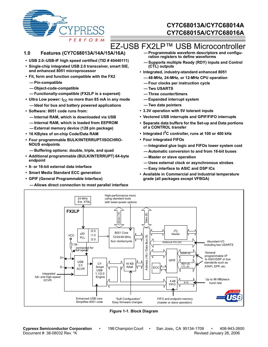 CY7C68013A(英文版)(CY7C68013A).pdf
 TechnicalReference_Dem.pdf