®
ISL83070E, ISL83071E, ISL83072E, ISL83073E,
ISL83075E, ISL83076E, ISL83077E, ISL83078E
FN6115.4
June 22, 2007
Data Sheet
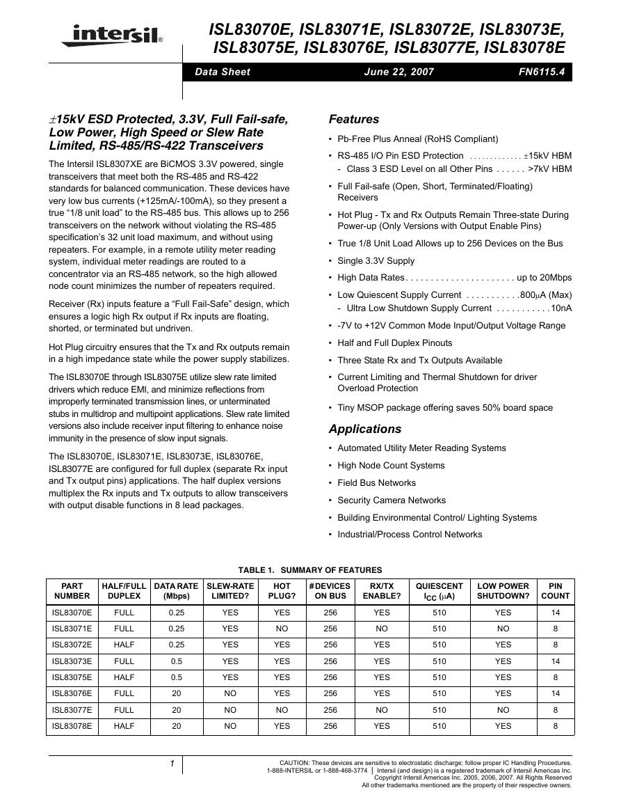
±15kV ESD Protected, 3.3V, Full Fail-safe,
Low Power, High Speed or Slew Rate
Limited, RS-485/RS-422 Transceivers
The Intersil ISL8307XE are BiCMOS 3.3V powered, single
transceivers that meet both the RS-485 and RS-422
standards for balanced communication. These devices have
very low bus currents (+125mA/-100mA), so they present a
true “1/8 unit load” to the RS-485 bus. This allows up to 256
transceivers on the network without violating the RS-485
specification’s 32 unit load maximum, and without using
repeaters. For example, in a remote utility meter reading
system, individual meter readings are routed to a
concentrator via an RS-485 network, so the high allowed
node count minimizes the number of repeaters required.
Receiver (Rx) inputs feature a “Full Fail-Safe” design, which
ensures a logic high Rx output if Rx inputs are floating,
shorted, or terminated but undriven.
Hot Plug circuitry ensures that the Tx and Rx outputs remain
in a high impedance state while the power supply stabilizes.
The ISL83070E through ISL83075E utilize slew rate limited
drivers which reduce EMI, and minimize reflections from
improperly terminated transmission lines, or unterminated
stubs in multidrop and multipoint applications. Slew rate limited
versions also include receiver input filtering to enhance noise
immunity in the presence of slow input signals.
The ISL83070E, ISL83071E, ISL83073E, ISL83076E,
ISL83077E are configured for full duplex (separate Rx input
and Tx output pins) applications. The half duplex versions
multiplex the Rx inputs and Tx outputs to allow transceivers
with output disable functions in 8 lead packages.
Features
• Pb-Free Plus Anneal (RoHS Compliant)
• RS-485 I/O Pin ESD Protection . . . . . . . . . . . . . ±15kV HBM
- Class 3 ESD Level on all Other Pins . . . . . . >7kV HBM
• Full Fail-safe (Open, Short, Terminated/Floating)
Receivers
• Hot Plug - Tx and Rx Outputs Remain Three-state During
Power-up (Only Versions with Output Enable Pins)
• True 1/8 Unit Load Allows up to 256 Devices on the Bus
• Single 3.3V Supply
• High Data Rates. . . . . . . . . . . . . . . . . . . . . . up to 20Mbps
• Low Quiescent Supply Current . . . . . . . . . . .800μA (Max)
- Ultra Low Shutdown Supply Current . . . . . . . . . . .10nA
• -7V to +12V Common Mode Input/Output Voltage Range
• Half and Full Duplex Pinouts
• Three State Rx and Tx Outputs Available
• Current Limiting and Thermal Shutdown for driver
Overload Protection
• Tiny MSOP package offering saves 50% board space
Applications
• Automated Utility Meter Reading Systems
• High Node Count Systems
• Field Bus Networks
• Security Camera Networks
• Building Environmental Control/ Lighting Systems
• Industrial/Process Control Networks
PART
NUMBER
ISL83070E
ISL83071E
ISL83072E
ISL83073E
ISL83075E
ISL83076E
ISL83077E
ISL83078E
HALF/FULL
DUPLEX
FULL
FULL
HALF
FULL
HALF
FULL
FULL
HALF
DATA RATE
(Mbps)
0.25
0.25
0.25
0.5
0.5
20
20
20
1
TABLE 1. SUMMARY OF FEATURES
SLEW-RATE
LIMITED?
HOT
PLUG?
# DEVICES
ON BUS
RX/TX
ENABLE?
QUIESCENT
ICC (μA)
LOW POWER
SHUTDOWN?
PIN
COUNT
YES
YES
YES
YES
YES
NO
NO
NO
YES
NO
YES
YES
YES
YES
NO
YES
256
256
256
256
256
256
256
256
YES
NO
YES
YES
YES
YES
NO
YES
510
510
510
510
510
510
510
510
YES
NO
YES
YES
YES
YES
NO
YES
14
8
8
14
8
14
8
8
CAUTION: These devices are sensitive to electrostatic discharge; follow proper IC Handling Procedures.
1-888-INTERSIL or 1-888-468-3774 | Intersil (and design) is a registered trademark of Intersil Americas Inc.
Copyright Intersil Americas Inc. 2005, 2006, 2007. All Rights Reserved
All other trademarks mentioned are the property of their respective owners.
�
ISL83070E, ISL83071E, ISL83072E, ISL83073E, ISL83075E, ISL83076E, ISL83077E, ISL83078E
Pinouts
ISL83072E, ISL83075E, ISL83078E
(8 LD MSOP, SOIC)
TOP VIEW
ISL83071E, ISL83077E
(8 LD SOIC)
TOP VIEW
ISL83070E, ISL83073E, ISL83076E
(14 LD SOIC)
TOP VIEW
RO
RE
DE
DI
1
2
3
4
R
D
8
7
6
5
VCC
B/Z
A/Y
GND
VCC
RO
DI
GND
1
2
3
4
R
D
8
7
6
5
A
B
Z
Y
NC
RO
RE
DE
DI
GND
GND
1
2
3
4
5
6
7
R
D
14
13
12
11
10
9
8
VCC
NC
A
B
Z
Y
NC
Ordering Information
PART NUMBER
(Notes 1, 2)
PART
MARKING
TEMP.
RANGE
(°C)
PACKAGE
(Pb-Free)
PKG.
DWG. #
ISL83070EIBZA 83070EIBZ -40 to 85 14 Ld SOIC M14.15
ISL83071EIBZA 83071 EIBZ -40 to 85 8 Ld SOIC M8.15
ISL83072EIBZA 83072 EIBZ -40 to 85 8 Ld SOIC M8.15
ISL83072EIUZA 3072Z
-40 to 85 8 Ld MSOP M8.118
ISL83073EIBZA 83073EIBZ -40 to 85 14 Ld SOIC M14.15
ISL83075EIBZA 83075 EIBZ -40 to 85 8 Ld SOIC M8.15
ISL83075EIUZA 3075Z
-40 to 85 8 Ld MSOP M8.118
ISL83076EIBZA 83076EIBZ -40 to 85 14 Ld SOIC M14.15
ISL83077EIBZA 83077 EIBZ -40 to 85 8 Ld SOIC M8.15
ISL83078EIBZA 83078 EIBZ -40 to 85 8 Ld SOIC M8.15
ISL83078EIUZA 3078Z
-40 to 85 8 Ld MSOP M8.118
NOTES:
1. Units also available in Tape and Reel; Add “-T” to suffix.
2. Intersil Pb-free plus anneal products employ special Pb-free
material sets; molding compounds/die attach materials and
100% matte tin plate termination finish, which are RoHS
compliant and compatible with both SnPb and Pb-free soldering
operations. Intersil Pb-free products are MSL classified at
Pb-free peak reflow temperatures that meet or exceed the
Pb-free requirements of IPC/JEDEC J STD-020.
Truth Tables
TRANSMITTING
INPUTS
DE
1
1
0
0
RE
X
X
0
1
DI
1
0
X
X
OUTPUTS
Z
0
1
Y
1
0
High-Z
High-Z*
High-Z
High-Z*
NOTE: *Shutdown Mode (See Note 9), except for ISL83071E/77E
RECEIVING
INPUTS
DE
DE
Half Duplex
Full Duplex
OUTPUT
RO
A-B
0
0
0
0
1
X
X
X
0
1
≥ -0.05V
≤ -0.2V
Inputs
Open/Shorted
1
0
1
X
X
High-Z*
High-Z
RE
0
0
0
1
1
NOTE: *Shutdown Mode (See Note 9), except for ISL83071E/77E
2
FN6115.4
June 22, 2007
�
ISL83070E, ISL83071E, ISL83072E, ISL83073E, ISL83075E, ISL83076E, ISL83077E, ISL83078E
Pin Descriptions
PIN
RO
RE
DE
DI
GND
A/Y
B/Z
A
B
Y
Z
VCC
NC
FUNCTION
Receiver output: If A - B ≥ -50mV, RO is high; If A - B ≤ -200mV, RO is low; RO = High if A and B are unconnected (floating) or shorted.
Receiver output enable. RO is enabled when RE is low; RO is high impedance when RE is high. If the Rx enable function isn’t
required, connect RE directly to GND or through a 1kΩ to 3kΩ resistor to GND.
Driver output enable. The driver outputs, Y and Z, are enabled by bringing DE high, and are high impedance when DE is low. If the
Tx enable function isn’t required, connect DE to VCC through a 1kΩ to 3kΩ resistor.
Driver input. A low on DI forces output Y low and output Z high. Similarly, a high on DI forces output Y high and output Z low.
Ground connection.
±15kV HBM ESD Protected RS-485/RS-422 level, noninverting receiver input and noninverting driver output. Pin is an input if DE =
0; pin is an output if DE = 1.
±15kV HBM ESD Protected RS-485/RS-422 level, Inverting receiver input and inverting driver output. Pin is an input if DE = 0; pin is
an output if DE = 1.
±15kV HBM ESD Protected RS-485/RS-422 level, noninverting receiver input.
±15kV HBM ESD Protected RS-485/RS-422 level, inverting receiver input.
±15kV HBM ESD Protected RS-485/RS-422 level, noninverting driver output.
±15kV HBM ESD Protected RS-485/RS-422 level, inverting driver output.
System power supply input (3.0V to 3.6V).
No Connection.
3
FN6115.4
June 22, 2007
�
ISL83070E, ISL83071E, ISL83072E, ISL83073E, ISL83075E, ISL83076E, ISL83077E, ISL83078E
Typical Operating Circuits
+3.3V
8
VCC
+
0.1μF
B/Z
A/Y
7
6
RT
GND
5
1
2
3
4
RO
RE
DE
DI
R
D
+
0.1μF
RT
+3.3V
1
VCC
A
B
Z
Y
8
7
6
5
GND
4
2
RO
R
3
DI
D
2
3
4
5
RO
RE
DE
DI
D
+3.3V
+
0.1μF
RT
14
R
VCC
A
B
12
11
Z
Y
10
9
GND
6, 7
4
ISL83072E, ISL83075E, ISL83078E
ISL83071E, ISL83077E
+
0.1μF
+3.3V
8
VCC
RT
7
6
B/Z
A/Y
GND
5
DI
DE
RE
RO
4
3
2
1
D
R
+
0.1μF
RT
+3.3V
1
VCC
5
6
7
8
Y
Z
B
A
GND
4
DI
3
D
RO
2
R
+
0.1μF
RT
+3.3V
14
VCC
D
R
9
10
11
12
Y
Z
B
A
GND
6, 7
DI
DE
RE
RO
5
4
3
2
ISL83070E, ISL83073E, ISL83076E
FN6115.4
June 22, 2007
�
ISL83070E, ISL83071E, ISL83072E, ISL83073E, ISL83075E, ISL83076E, ISL83077E, ISL83078E
Absolute Maximum Ratings
VCC to Ground. . . . . . . . . . . . . . . . . . . . . . . . . . . . . . . . . . . . . . . 7V
Input Voltages
DI, DE, RE . . . . . . . . . . . . . . . . . . . . . . . . . . . . . . . . . -0.3V to 7V
Input/Output Voltages
A, B, Y, Z . . . . . . . . . . . . . . . . . . . . . . . . . . . . . . . . . . -9V to +13V
RO . . . . . . . . . . . . . . . . . . . . . . . . . . . . . . . . -0.3V to (VCC +0.3V)
Short Circuit Duration
Y, Z . . . . . . . . . . . . . . . . . . . . . . . . . . . . . . . . . . . . . . . Continuous
ESD Rating . . . . . . . . . . . . . . . . . . . . . . . . . See Specification Table
Thermal Information
Thermal Resistance (Typical, Note 3)
θJA (°C/W)
8 Ld SOIC Package . . . . . . . . . . . . . . . . . . . . . . . . .
8 Ld MSOP Package . . . . . . . . . . . . . . . . . . . . . . . .
14 Ld SOIC Package . . . . . . . . . . . . . . . . . . . . . . . .
105
140
128
Maximum Junction Temperature (Plastic Package) . . . . . . +150°C
Maximum Storage Temperature Range. . . . . . . . . .-65°C to +150°C
Pb-free reflow profile . . . . . . . . . . . . . . . . . . . . . . . . . .see link below
http://www.intersil.com/pbfree/Pb-FreeReflow.asp
Operating Conditions
Temperature Range . . . . . . . . . . . . . . . . . . . . . . . . . .-40°C to +85°C
CAUTION: Do not operate at or near the maximum ratings listed for extended periods of time. Exposure to such conditions may adversely impact product reliability and
result in failures not covered by warranty.
NOTE:
3. θJA is measured with the component mounted on a high effective thermal conductivity test board in free air. See Tech Brief TB379 for details.
Electrical Specifications
Test Conditions: VCC = 3.0V to 3.6V; Unless Otherwise Specified.
Typicals are at VCC = 3.3V, TA = +25°C (Note 4).
PARAMETER
DC CHARACTERISTICS
Driver Differential VOUT
Change in Magnitude of Driver
Differential VOUT for
Complementary Output States
Driver Common-Mode VOUT
Change in Magnitude of Driver
Common-Mode VOUT for
Complementary Output States
Logic Input High Voltage
Logic Input Low Voltage
Logic Input Hysteresis
Logic Input Current
Input Current (A, B, A/Y, B/Z)
Output Leakage Current (Y, Z) (Full
Duplex Versions Only, Note 12)
Output Leakage Current (Y, Z)
in Shutdown Mode (Full Duplex,
Note 12)
Driver Short-Circuit Current,
VO = High or Low
Receiver Differential Threshold
Voltage
Receiver Input Hysteresis
Receiver Output High Voltage
5
SYMBOL
TEST CONDITIONS
TEMP
(°C)
MIN
(Note 18) TYP
MAX
(Note 18) UNITS
VOD
ΔVOD
RL = 100Ω (RS-422) (Figure 1A, Note 15)
RL = 54Ω (RS-485) (Figure 1A)
No Load
RL = 60Ω, -7V ≤ VCM ≤ 12V (Figure 1B)
RL = 54Ω or 100Ω (Figure 1A)
VOC
ΔVOC
RL = 54Ω or 100Ω (Figure 1A)
RL = 54Ω or 100Ω (Figure 1A)
VIH
VIL
VHYS
IIN1
IIN2
IIN3
IIN4
DI, DE, RE
DI, DE, RE
DE, RE, (Note 14)
DI = DE = RE = 0V or VCC, (Note 17)
VIN = 12V
DE = 0V, VCC = 0V or
3.6V
VIN = -7V
VIN = 12V
VIN = -7V
VIN = 12V
VIN = -7V
RE = VCC, DE = 0V,
VCC = 0V or 3.6V
RE = 0V, DE = 0V,
VCC = 0V or 3.6V
IOSD1
DE = VCC, -7V ≤ VY or VZ ≤ 12V (Note 6)
VTH
-7V ≤ VCM ≤ 12V
ΔVTH
VOH
VCM = 0V
IO = -4mA, VID = -50mV
Full
Full
Full
Full
Full
Full
Full
Full
25
Full
Full
Full
Full
Full
Full
Full
Full
Full
25
Full
2
1.5
-
1.5
-
-
-
2
-
-
-2
-
-100
-
-40
-
-40
-
2.3
2
-
2.2
0.01
2
0.01
-
-
100
-
80
-50
10
-10
10
-10
-
-
VCC
VCC
-
0.2
3
0.2
-
0.8
-
2
125
-
40
-
40
-
±250
-200
-125
-50
-
VCC - 0.6
15
-
-
-
V
V
V
V
V
V
V
V
mV
μA
μA
μA
μA
μA
μA
μA
mA
mV
mV
V
FN6115.4
June 22, 2007
�
ISL83070E, ISL83071E, ISL83072E, ISL83073E, ISL83075E, ISL83076E, ISL83077E, ISL83078E
Electrical Specifications
Test Conditions: VCC = 3.0V to 3.6V; Unless Otherwise Specified.
Typicals are at VCC = 3.3V, TA = +25°C (Note 4).
PARAMETER
SYMBOL
TEST CONDITIONS
Receiver Output Low Voltage
Three-State (high impedance)
Receiver Output Current (Note 12)
Receiver Input Resistance
Receiver Short-Circuit Current
Thermal Shutdown Threshold
SUPPLY CURRENT
No-Load Supply Current (Note 5)
IO = -4mA, VID = -200mV
0.4V ≤ VO ≤ 2.4V
-7V ≤ VCM ≤ 12V
0V ≤ VO ≤ VCC
VOL
IOZR
RIN
IOSR
TSD
ICC
DI = 0V or VCC
DE = VCC,
RE = 0V or VCC
DE = 0V, RE = 0V
ISHDN
DE = 0V, RE = VCC, DI = 0V or VCC
Shutdown Supply Current
(Note 12)
ESD PERFORMANCE
RS-485 Pins (A, Y, B, Z)
All Other Pins
DRIVER SWITCHING CHARACTERISTICS (ISL83070E, ISL83071E, ISL83072E, 250kbps)
Maximum Data Rate
Driver Differential Output Delay
Driver Differential Output Skew
Driver Differential Rise or Fall Time
Driver Enable to Output High
Human Body Model (HBM), Pin to GND
HBM, per MIL-STD-883 Method 3015
fMAX
tDD
tSKEW
tR, tF
tZH
VOD = ±1.5V, CD = 820pF (Figure 4, Note 16)
RDIFF = 54Ω, CD = 50pF (Figure 2)
RDIFF = 54Ω, CD = 50pF (Figure 2)
RDIFF = 54Ω, CD = 50pF (Figure 2)
RL = 500Ω, CL = 50pF, SW = GND (Figure 3),
(Notes 7, 12)
RL = 500Ω, CL = 50pF, SW = VCC (Figure 3),
(Notes 7, 12)
RL = 500Ω, CL = 50pF, SW = GND (Figure 3),
(Note 12)
RL = 500Ω, CL = 50pF, SW = VCC (Figure 3),
(Note 12)
(Notes 9, 12)
Driver Enable to Output Low
Driver Disable from Output High
Driver Disable from Output Low
tZL
tHZ
tLZ
tZH(SHDN) RL = 500Ω, CL = 50pF, SW = GND (Figure 3),
tZL(SHDN) RL = 500Ω, CL = 50pF, SW = VCC (Figure 3),
tSHDN
(Notes 9, 10, 12)
Time to Shutdown
Driver Enable from Shutdown to
Output High
Driver Enable from Shutdown to
Output Low
DRIVER SWITCHING CHARACTERISTICS (ISL83073E, ISL83075E, 500kbps)
Maximum Data Rate
Driver Differential Output Delay
Driver Differential Output Skew
Driver Differential Rise or Fall Time
Driver Enable to Output High
fMAX
tDD
tSKEW
tR, tF
tZH
(Notes 9, 10, 12)
VOD = ±1.5V, CD = 820pF (Figure 4, Note 16)
RDIFF = 54Ω, CD = 50pF (Figure 2)
RDIFF = 54Ω, CD = 50pF (Figure 2)
RDIFF = 54Ω, CD = 50pF (Figure 2)
RL = 500Ω, CL = 50pF, SW = GND (Figure 3),
(Notes 7, 12)
RL = 500Ω, CL = 50pF, SW = VCC (Figure 3),
(Notes 7, 12)
RL = 500Ω, CL = 50pF, SW = GND (Figure 3),
(Note 12)
TEMP
(°C)
Full
Full
Full
Full
Full
Full
Full
Full
25
25
Full
Full
Full
Full
Full
Full
Full
Full
Full
Full
Full
Full
Full
Full
Full
Full
Full
Full
MIN
(Note 18) TYP
0.17
0.015
-
-1
96
±7
-
-
-
-
-
−
250
250
-
350
-
-
-
-
50
-
-
500
180
-
200
-
-
-
150
30
150
510
480
0.01
±15
>±7
800
1100
6
960
26
200
28
30
200
180
100
1600
350
1
380
26
100
28
MAX
(Note 18) UNITS
0.4
1
-
±60
-
800
700
1
-
-
-
1500
100
1600
600
600
55
55
600
700
700
-
800
30
800
350
350
55
V
μA
kΩ
mA
°C
μA
μA
μA
kV
kV
kbps
ns
ns
ns
ns
ns
ns
ns
ns
ns
ns
kbps
ns
ns
ns
ns
ns
ns
Driver Enable to Output Low
Driver Disable from Output High
tZL
tHZ
6
FN6115.4
June 22, 2007
�
ISL83070E, ISL83071E, ISL83072E, ISL83073E, ISL83075E, ISL83076E, ISL83077E, ISL83078E
Electrical Specifications
Test Conditions: VCC = 3.0V to 3.6V; Unless Otherwise Specified.
Typicals are at VCC = 3.3V, TA = +25°C (Note 4).
PARAMETER
Driver Disable from Output Low
SYMBOL
tLZ
TEST CONDITIONS
RL = 500Ω, CL = 50pF, SW = VCC (Figure 3),
(Note 12)
(Notes 9, 12)
tSHDN
(Notes 9, 10, 12)
tZH(SHDN) RL = 500Ω, CL = 50pF, SW = GND (Figure 3),
tZL(SHDN) RL = 500Ω, CL = 50pF, SW = VCC (Figure 3),
Time to Shutdown
Driver Enable from Shutdown to
Output High
Driver Enable from Shutdown to
Output Low
DRIVER SWITCHING CHARACTERISTICS (ISL83076E, ISL83077E, ISL83078E, 20Mbps)
Maximum Data Rate
Driver Differential Output Delay
Driver Differential Output Skew
Driver Output Skew, Part-to-Part
Driver Differential Rise or Fall Time
Driver Enable to Output High
fMAX
tDD
tSKEW
ΔtDSKEW RDIFF = 54Ω, CD = 50pF (Figure 2, Note 13)
VOD = ±1.5V, CD = 350pF (Figure 4, Note 16)
RDIFF = 54Ω, CD = 50pF (Figure 2)
RDIFF = 54Ω, CD = 50pF (Figure 2)
(Notes 9, 10, 12)
tR, tF
tZH
Driver Enable to Output Low
Driver Disable from Output High
Driver Disable from Output Low
tZL
tHZ
tLZ
RDIFF = 54Ω, CD = 50pF (Figure 2)
RL = 500Ω, CL = 50pF, SW = GND (Figure 3),
(Notes 7, 12)
RL = 500Ω, CL = 50pF, SW = VCC (Figure 3),
(Notes 7, 12)
RL = 500Ω, CL = 50pF, SW = GND (Figure 3),
(Note 12)
RL = 500Ω, CL = 50pF, SW = VCC (Figure 3),
(Note 12)
(Notes 9, 12)
tSHDN
Time to Shutdown
Driver Enable from Shutdown to
Output High
Driver Enable from Shutdown to
Output Low
RECEIVER SWITCHING CHARACTERISTICS (All Versions)
Maximum Data Rate
fMAX
(Notes 9, 10, 12)
(Notes 9, 10, 12)
VID = ±1.5V (Note 16)
tZH(SHDN) RL = 500Ω, CL = 50pF, SW = GND (Figure 3),
tZL(SHDN) RL = 500Ω, CL = 50pF, SW = VCC (Figure 3),
Receiver Input to Output Delay
tPLH, tPHL (Figure 5)
Receiver Skew | tPLH - tPHL |
Receiver Skew, Part-to-Part
Receiver Enable to Output High
Receiver Enable to Output Low
Receiver Disable from Output High
Receiver Disable from Output Low
tSKD
(Figure 5)
ΔtRSKEW (Figure 5, Note 13)
tZH
tZL
tHZ
tLZ
RL = 1kΩ, CL = 15pF,
SW = GND (Figure 6),
(Notes 8, 12)
RL = 1kΩ, CL = 15pF,
SW = VCC (Figure 6),
(Notes 8, 12)
RL = 1kΩ, CL = 15pF,
SW = GND (Figure 6),
(Note 12)
RL = 1kΩ, CL = 15pF,
SW = VCC (Figure 6),
(Note 12)
(Notes 9, 12)
Time to Shutdown
tSHDN
7
ISL83070E-75E
ISL83076E-78E
ISL83070E-75E
ISL83076E-78E
ISL83070E-75E
ISL83076E-78E
ISL83070E-75E
ISL83076E-78E
ISL83070E-75E
ISL83076E-78E
ISL83070E-75E
ISL83076E-78E
MIN
(Note 18) TYP
30
-
50
-
-
20
-
-
-
-
-
-
-
-
50
-
-
12
20
25
25
-
-
5
5
5
5
5
4
5
4
200
180
100
28
27
1
-
9
17
16
25
28
200
180
90
20
35
70
33
1.5
-
15
11
15
11
12
7
13
7
TEMP
(°C)
Full
Full
Full
Full
Full
Full
Full
Full
Full
Full
Full
Full
Full
Full
Full
Full
Full
Full
Full
Full
Full
Full
Full
Full
Full
Full
Full
Full
Full
Full
Full
MAX
(Note 18) UNITS
55
600
700
700
-
40
3
11
15
50
40
40
50
600
700
700
-
-
120
60
4
15
20
17
20
17
20
15
20
15
ns
ns
ns
ns
Mbps
ns
ns
ns
ns
ns
ns
ns
ns
ns
ns
ns
Mbps
Mbps
ns
ns
ns
ns
ns
ns
ns
ns
ns
ns
ns
ns
ns
FN6115.4
June 22, 2007
50
180
600
�
ISL83070E, ISL83071E, ISL83072E, ISL83073E, ISL83075E, ISL83076E, ISL83077E, ISL83078E
Electrical Specifications
Test Conditions: VCC = 3.0V to 3.6V; Unless Otherwise Specified.
Typicals are at VCC = 3.3V, TA = +25°C (Note 4).
PARAMETER
SYMBOL
tZH(SHDN) RL = 1kΩ, CL = 15pF, SW = GND (Figure 6),
TEST CONDITIONS
Receiver Enable from Shutdown to
Output High
Receiver Enable from Shutdown to
Output Low
NOTES:
4. All currents into device pins are positive; all currents out of device pins are negative. All voltages are referenced to device ground unless otherwise
tZL(SHDN) RL = 1kΩ, CL = 15pF, SW = VCC (Figure 6),
(Notes 9, 11, 12)
(Notes 9, 11, 12)
500
ns
ns
Full
-
240
500
TEMP
(°C)
Full
MIN
(Note 18) TYP
240
-
MAX
(Note 18) UNITS
specified.
5. Supply current specification is valid for loaded drivers when DE = 0V.
6. Applies to peak current. See “Typical Performance Curves” for more information.
7. When testing devices with the shutdown feature, keep RE = 0 to prevent the device from entering SHDN.
8. When testing devices with the shutdown feature, the RE signal high time must be short enough (typically <100ns) to prevent the device from
entering SHDN.
9. Versions with a shutdown feature are put into shutdown by bringing RE high and DE low. If the inputs are in this state for less than 50ns, the parts
are guaranteed not to enter shutdown. If the inputs are in this state for at least 600ns, the parts are guaranteed to have entered shutdown. See
“Low Power Shutdown Mode” on page 11.
10. Keep RE = VCC, and set the DE signal low time >600ns to ensure that the device enters SHDN.
11. Set the RE signal high time >600ns to ensure that the device enters SHDN.
12. Does not apply to the ISL83071E and ISL83077E.
13. ΔtSKEW is the magnitude of the difference in propagation delays of the specified terminals of two units tested with identical test conditions (VCC,
temperature, etc.). Only applies to the ISL83076E - 78E.
14. ISL83070E - ISL83075E only.
15. VCC ≥ 3.15V
16. Limits established by characterization and are not production tested.
17. If the Tx or Rx enable function isn’t needed, connect the enable pin to the appropriate supply (see “Pin Descriptions” table) through a 1kΩ to 3kΩ
resistor.
18. Parts are 100% tested at +25°C. Full temperature limits are guaranteed by bench and tester characterization.
Test Circuits and Waveforms
VCC
DE
DI
D
Z
Y
VOD
RL/2
RL/2
VOC
VCC
DE
DI
D
Z
Y
VOD
RL = 60Ω
375Ω
VCM
-7V TO +12V
375Ω
FIGURE 1A. VOD AND VOC
FIGURE 1B. VOD WITH COMMON MODE LOAD
FIGURE 1. DC DRIVER TEST CIRCUITS
8
FN6115.4
June 22, 2007
�


 V2版本原理图(Capacitive-Fingerprint-Reader-Schematic_V2).pdf
 摄像头工作原理.doc
 VL53L0X简要说明(En.FLVL53L00216).pdf
 原理图(DVK720-Schematic).pdf
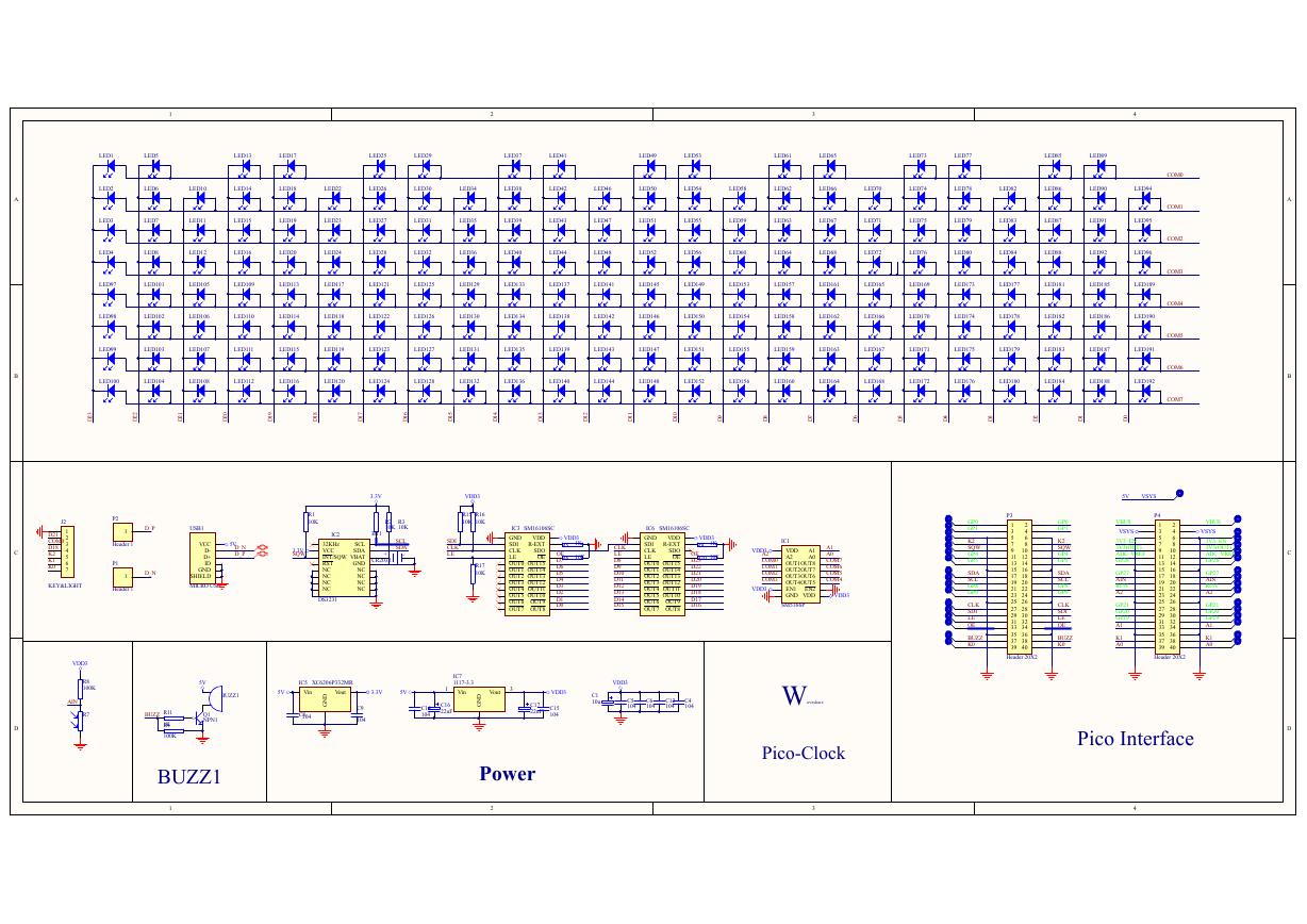 原理图(Pico-Clock-Green-Schdoc).pdf
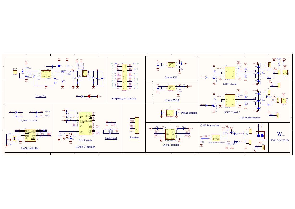 原理图(RS485-CAN-HAT-B-schematic).pdf
 File:SIM7500_SIM7600_SIM7800 Series_SSL_Application Note_V2.00.pdf
 ADS1263(Ads1262).pdf
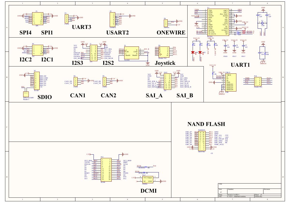 原理图(Open429Z-D-Schematic).pdf
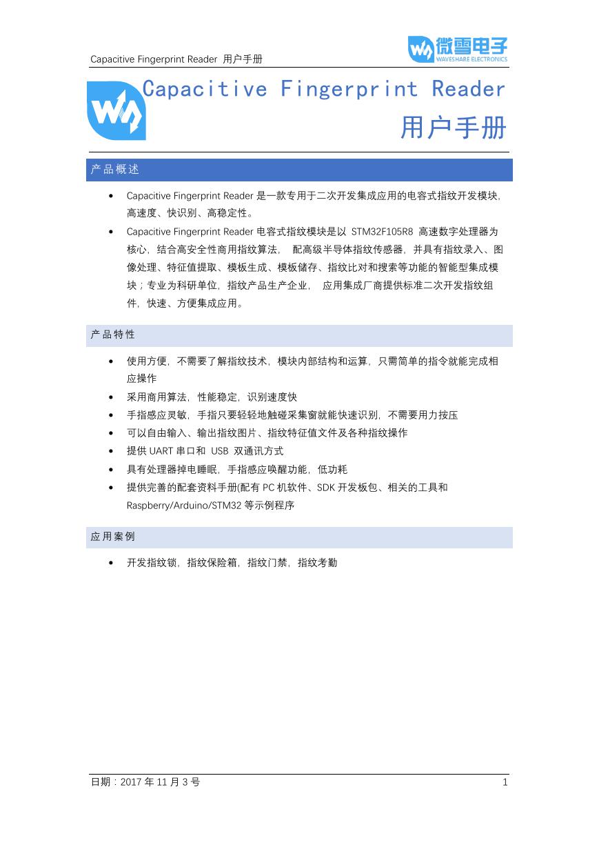 用户手册(Capacitive_Fingerprint_Reader_User_Manual_CN).pdf
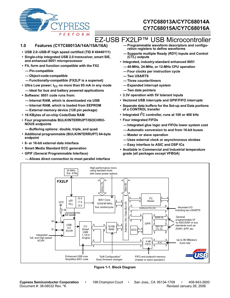 CY7C68013A(英文版)(CY7C68013A).pdf
 TechnicalReference_Dem.pdf