V0.1
Data Sheet
RTC6603SP
Oct 2013
RTC6603SP : 0.1 GHz – 3.0 GHz SPDT Switch
Description
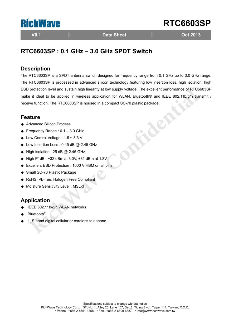
The RTC6603SP is a SPDT antenna switch designed for frequency range from 0.1 GHz up to 3.0 GHz range.
The RTC6603SP is processed in advanced silicon technology featuring low insertion loss, high isolation, high
ESD protection level and sustain high linearity at low supply voltage. The excellent performance of RTC6603SP
make it ideal to be applied in wireless application for WLAN, Bluetooth® and IEEE 802.11b/g/n transmit /
receive function. The RTC6603SP is housed in a compact SC-70 plastic package.
Feature
◆ Advanced Silicon Process
◆ Frequency Range : 0.1 – 3.0 GHz
◆ Low Control Voltage : 1.6 ~ 3.3 V
◆ Low Insertion Loss : 0.45 dB @ 2.45 GHz
◆ High Isolation : 25 dB @ 2.45 GHz
◆ High P1dB : +32 dBm at 3.0V, +31 dBm at 1.8V
◆ Excellent ESD Protection : 1000 V HBM on all pins
◆ Small SC-70 Plastic Package
◆ RoHS, Pb-free, Halogen Free Compliant
◆ Moisture Sensitivity Level : MSL-3
Application
IEEE 802.11b/g/n WLAN networks
◆
◆ Bluetooth®
◆ L, S band digital cellular or cordless telephone
Specifications subject to change without notice
1
RichWave Technology Corp. 3F, No. 1, Alley 20, Lane 407, Sec.2, Tiding Blvd., Taipei 114, Taiwan, R.O.C.
• Phone : +886-2-8751-1358 • Fax : +886-2-6600-6887 • Info@www.richwave.com.tw
RichWave Confidential�
V0.1
Data Sheet
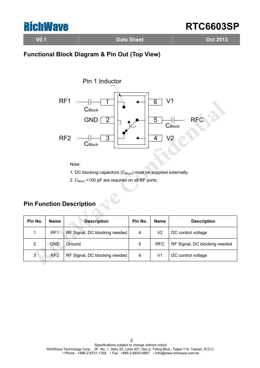
Functional Block Diagram & Pin Out (Top View)
Pin 1 Inductor
RTC6603SP
Oct 2013
RF1
RF2
1
2
3
CBlock
GND
CBlock
6
5
4
V1
CBlock
V2
RFC
Note:
1. DC blocking capacitors (CBlock) must be supplied externally.
2. CBlock =100 pF are required on all RF ports.
Pin Function Description
Pin No. Name
Description
Pin No.
Name
Description
1
2
3
RF1 RF Signal, DC blocking needed
GND Ground
RF2 RF Signal, DC blocking needed
4
5
6
V2
DC control voltage
RFC RF Signal, DC blocking needed
V1
DC control voltage
Specifications subject to change without notice
2
RichWave Technology Corp. 3F, No. 1, Alley 20, Lane 407, Sec.2, Tiding Blvd., Taipei 114, Taiwan, R.O.C.
• Phone : +886-2-8751-1358 • Fax : +886-2-6600-6887 • Info@www.richwave.com.tw
RichWave Confidential�
V0.1
Data Sheet
RTC6603SP
Oct 2013
Recommended Operation Range
Parameter
Symbol
Operation Frequency
f1
Control Voltage High (H)
V1, V2
V1, V2
Control Voltage Low (L)
Absolute Maximum Rating
Parameter
Control voltage
Input power
Operating temperature
Storage temperature
ESD (HBM, JESD22-A114, All pin)
ESD (CDM, JESD22-C101, All pin)
Maximum junction temperature
Min
0.1
1.6
0
Symbol
V1, V2
PIN
TA
TST
ESDHBM
ESDCDM
TJ
Typ
–
3.0
0
Max
3.0
3.3
0.4
Rating
+4.0
+30
-30 ~ +85
-30 ~ +125
1000
1000
125
Unit
GHz
V
V
Unit
V
dBm
℃
℃
V
V
℃
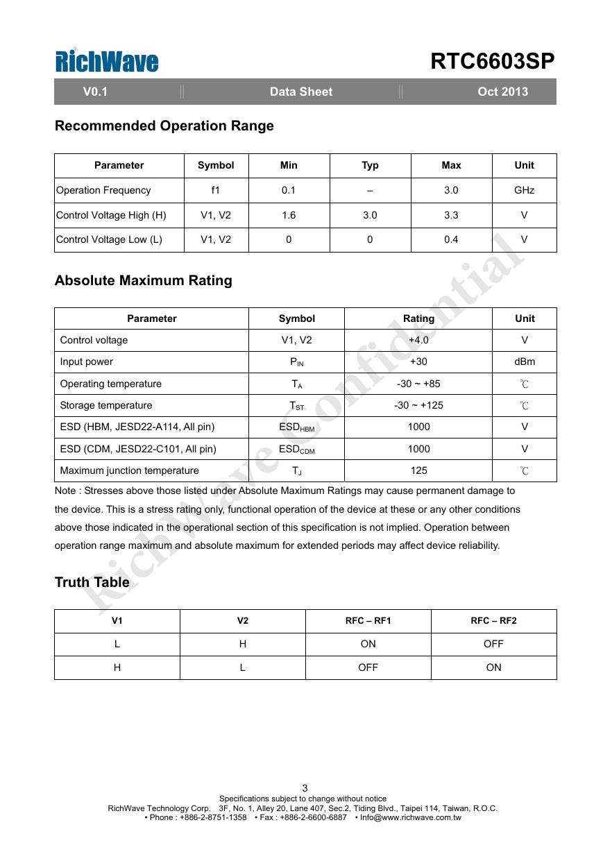
Note : Stresses above those listed under Absolute Maximum Ratings may cause permanent damage to
the device. This is a stress rating only, functional operation of the device at these or any other conditions
above those indicated in the operational section of this specification is not implied. Operation between
operation range maximum and absolute maximum for extended periods may affect device reliability.
Truth Table
V1
L
H
V2
H
L
RFC – RF1
RFC – RF2
ON
OFF
OFF
ON
Specifications subject to change without notice
3
RichWave Technology Corp. 3F, No. 1, Alley 20, Lane 407, Sec.2, Tiding Blvd., Taipei 114, Taiwan, R.O.C.
• Phone : +886-2-8751-1358 • Fax : +886-2-6600-6887 • Info@www.richwave.com.tw
RichWave Confidential�
V0.1
Data Sheet
RTC6603SP
Oct 2013
Electrical Specifications
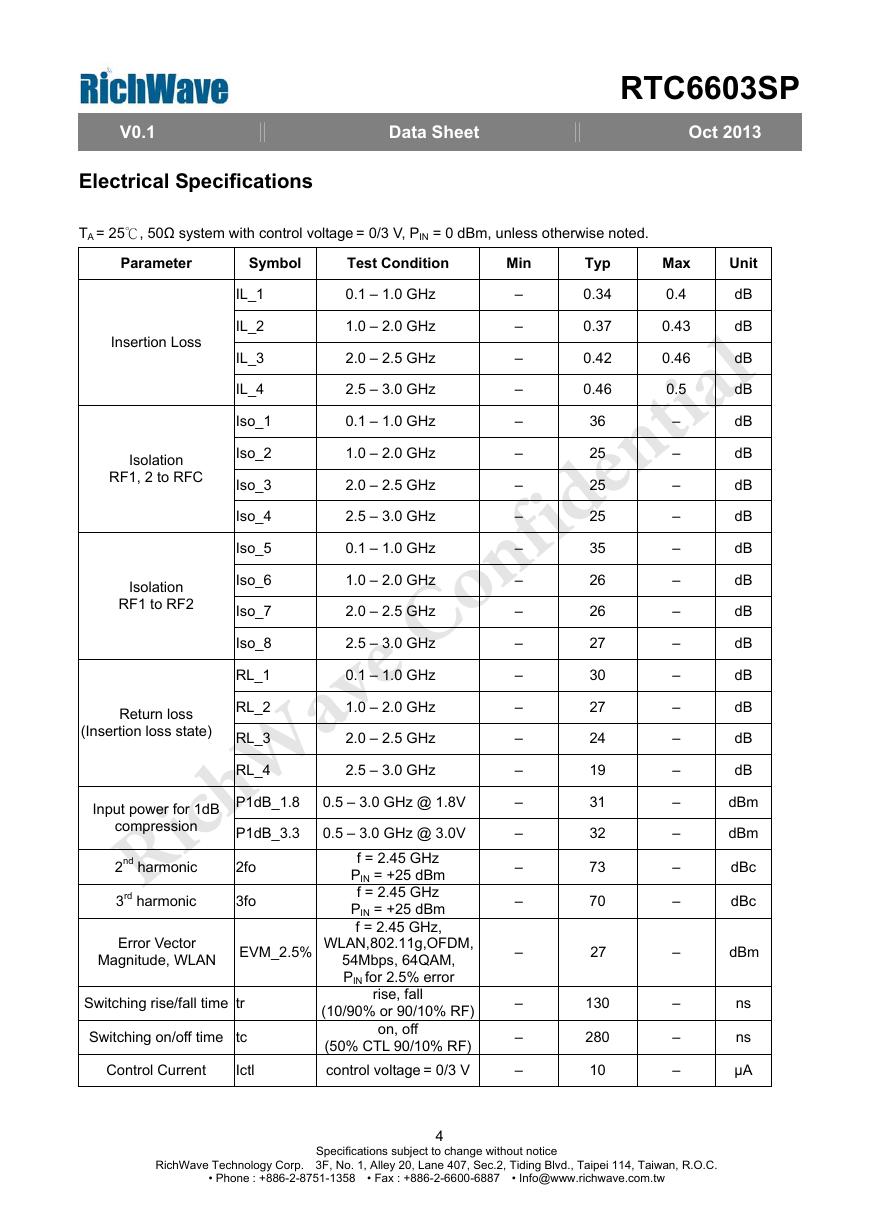
TA = 25℃, 50Ω system with control voltage = 0/3 V, PIN = 0 dBm, unless otherwise noted.
Parameter
Symbol
Test Condition
Min
Insertion Loss
Isolation
RF1, 2 to RFC
Isolation
RF1 to RF2
Return loss
(Insertion loss state)
IL_1
IL_2
IL_3
IL_4
Iso_1
Iso_2
Iso_3
Iso_4
Iso_5
Iso_6
Iso_7
Iso_8
RL_1
RL_2
RL_3
RL_4
0.1 – 1.0 GHz
1.0 – 2.0 GHz
2.0 – 2.5 GHz
2.5 – 3.0 GHz
0.1 – 1.0 GHz
1.0 – 2.0 GHz
2.0 – 2.5 GHz
2.5 – 3.0 GHz
0.1 – 1.0 GHz
1.0 – 2.0 GHz
2.0 – 2.5 GHz
2.5 – 3.0 GHz
0.1 – 1.0 GHz
1.0 – 2.0 GHz
2.0 – 2.5 GHz
2.5 – 3.0 GHz
Input power for 1dB
compression
P1dB_1.8
0.5 – 3.0 GHz @ 1.8V
P1dB_3.3
0.5 – 3.0 GHz @ 3.0V
2nd harmonic
3rd harmonic
2fo
3fo
Error Vector
Magnitude, WLAN EVM_2.5%
Switching rise/fall time tr
Switching on/off time
tc
Control Current
Ictl
f = 2.45 GHz
PIN = +25 dBm
f = 2.45 GHz
PIN = +25 dBm
f = 2.45 GHz,
WLAN,802.11g,OFDM,
54Mbps, 64QAM,
PIN for 2.5% error
rise, fall
(10/90% or 90/10% RF)
on, off
(50% CTL 90/10% RF)
control voltage = 0/3 V
–
–
–
–
–
–
–
–
–
–
–
–
–
–
–
–
–
–
–
–
–
–
–
–
Typ
0.34
0.37
0.42
0.46
36
25
25
25
35
26
26
27
30
27
24
19
31
32
73
70
27
130
280
10
Max
0.4
0.43
0.46
0.5
–
–
–
–
–
–
–
–
–
–
–
–
–
–
–
–
–
–
–
–
RichWave Technology Corp. 3F, No. 1, Alley 20, Lane 407, Sec.2, Tiding Blvd., Taipei 114, Taiwan, R.O.C.
• Phone : +886-2-8751-1358 • Fax : +886-2-6600-6887 • Info@www.richwave.com.tw
Specifications subject to change without notice
4
Unit
dB
dB
dB
dB
dB
dB
dB
dB
dB
dB
dB
dB
dB
dB
dB
dB
dBm
dBm
dBc
dBc
dBm
ns
ns
μA
RichWave Confidential�
V0.1
Data Sheet
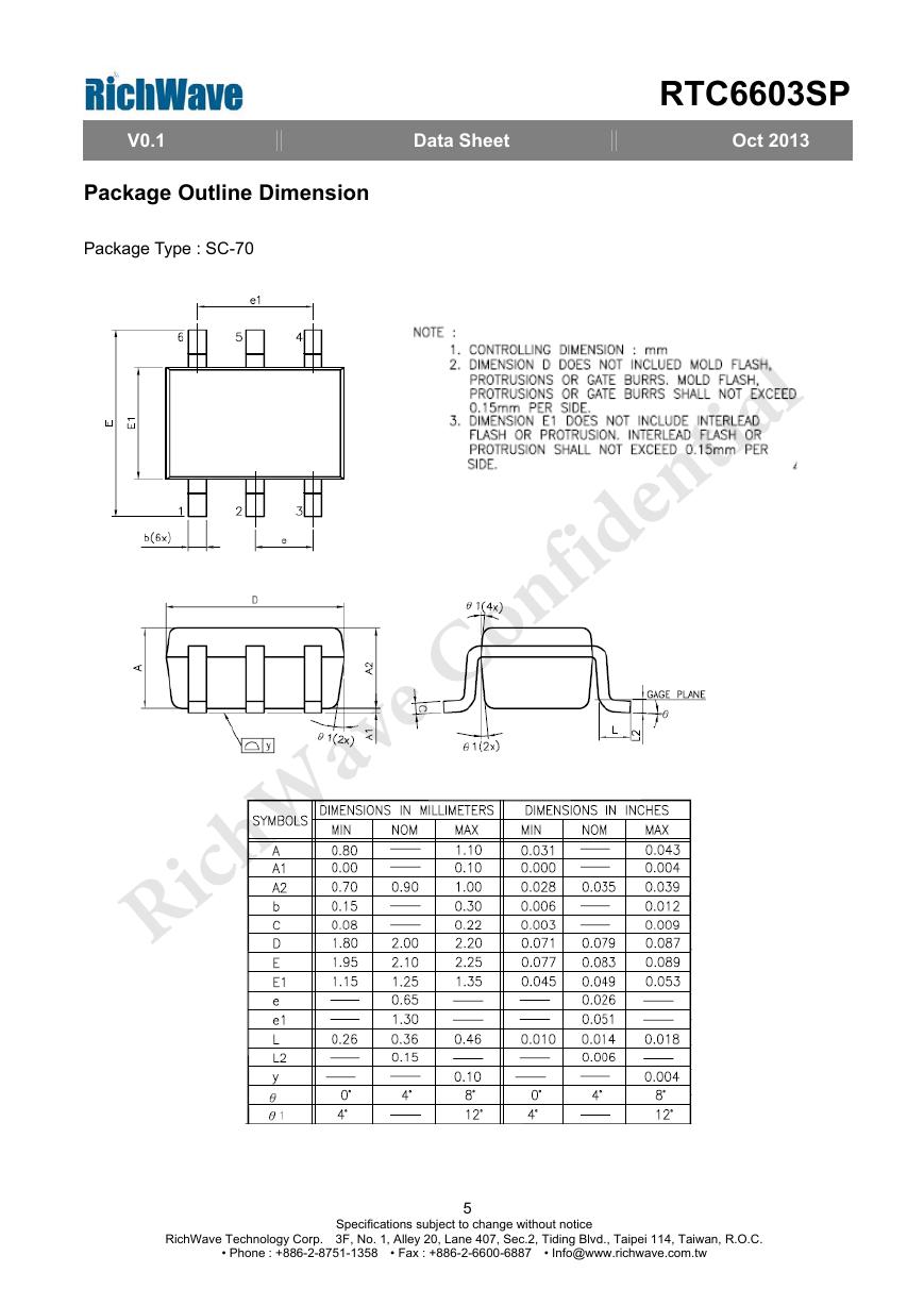
Package Outline Dimension
Package Type : SC-70
RTC6603SP
Oct 2013
Specifications subject to change without notice
5
RichWave Technology Corp. 3F, No. 1, Alley 20, Lane 407, Sec.2, Tiding Blvd., Taipei 114, Taiwan, R.O.C.
• Phone : +886-2-8751-1358 • Fax : +886-2-6600-6887 • Info@www.richwave.com.tw
RichWave Confidential�
RTC6603SP
Oct 2013
V0.1
Data Sheet
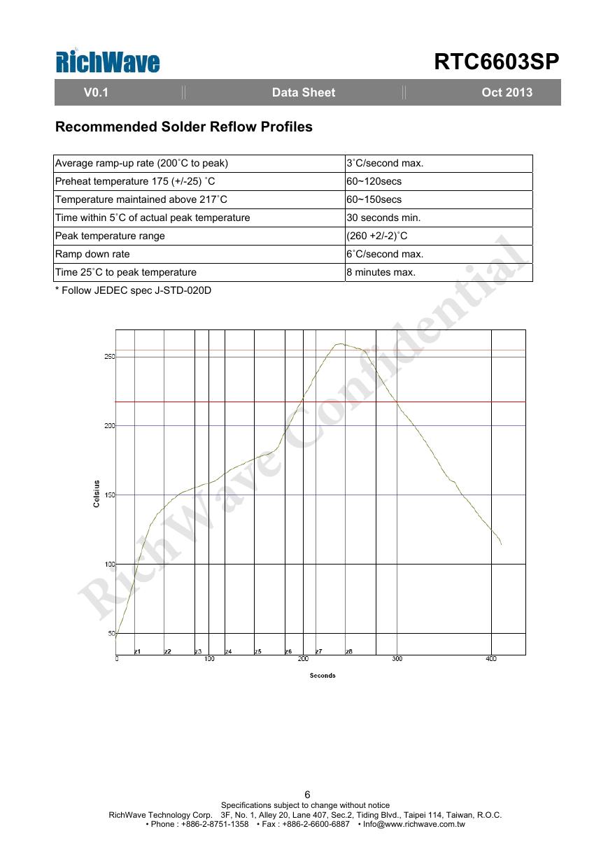
Recommended Solder Reflow Profiles
Average ramp-up rate (200˚C to peak)
Preheat temperature 175 (+/-25) ˚C
Temperature maintained above 217˚C
Time within 5˚C of actual peak temperature
Peak temperature range
Ramp down rate
Time 25˚C to peak temperature
* Follow JEDEC spec J-STD-020D
3˚C/second max.
60~120secs
60~150secs
30 seconds min.
(260 +2/-2)˚C
6˚C/second max.
8 minutes max.
Specifications subject to change without notice
6
RichWave Technology Corp. 3F, No. 1, Alley 20, Lane 407, Sec.2, Tiding Blvd., Taipei 114, Taiwan, R.O.C.
• Phone : +886-2-8751-1358 • Fax : +886-2-6600-6887 • Info@www.richwave.com.tw
RichWave Confidential�


 V2版本原理图(Capacitive-Fingerprint-Reader-Schematic_V2).pdf
 摄像头工作原理.doc
 VL53L0X简要说明(En.FLVL53L00216).pdf
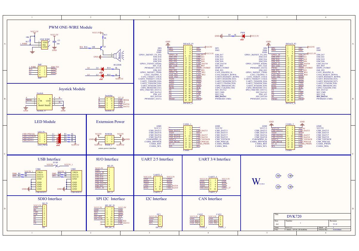 原理图(DVK720-Schematic).pdf
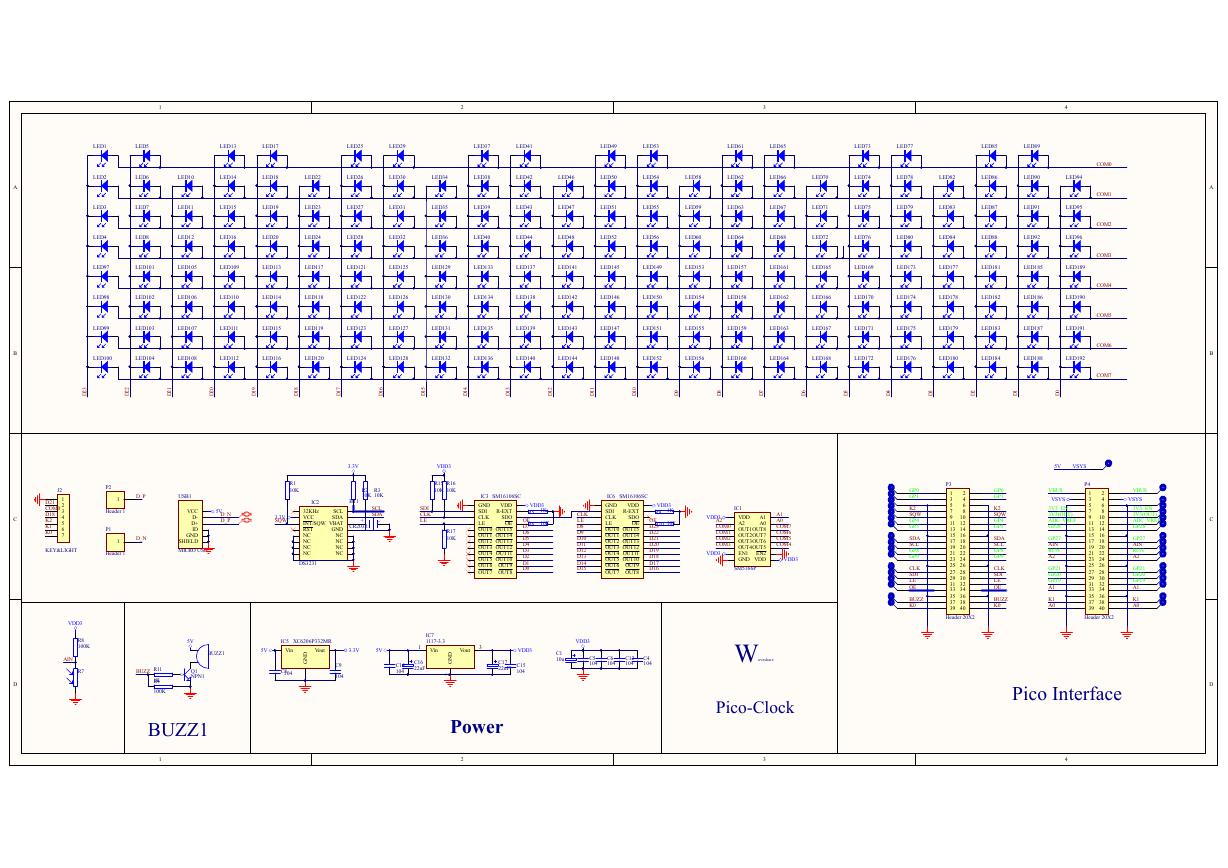 原理图(Pico-Clock-Green-Schdoc).pdf
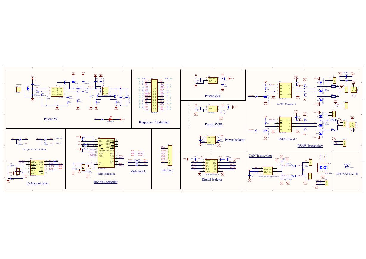 原理图(RS485-CAN-HAT-B-schematic).pdf
 File:SIM7500_SIM7600_SIM7800 Series_SSL_Application Note_V2.00.pdf
 ADS1263(Ads1262).pdf
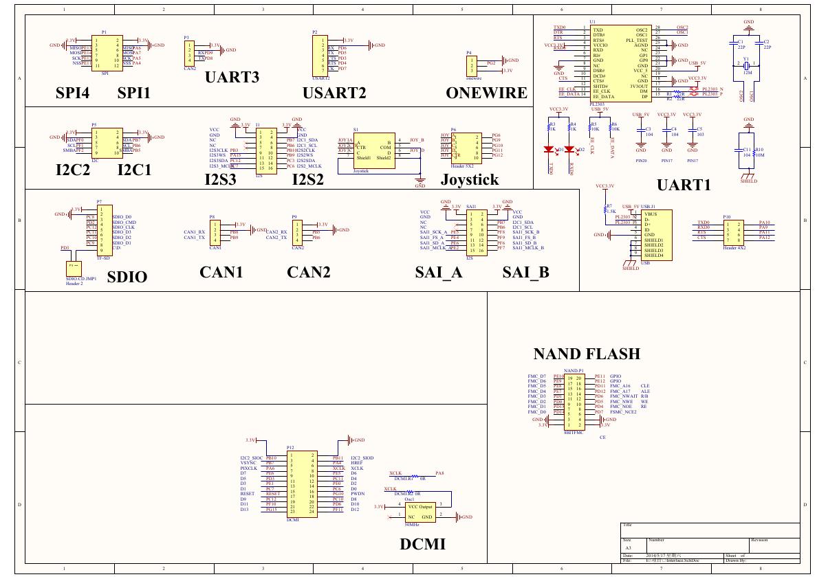 原理图(Open429Z-D-Schematic).pdf
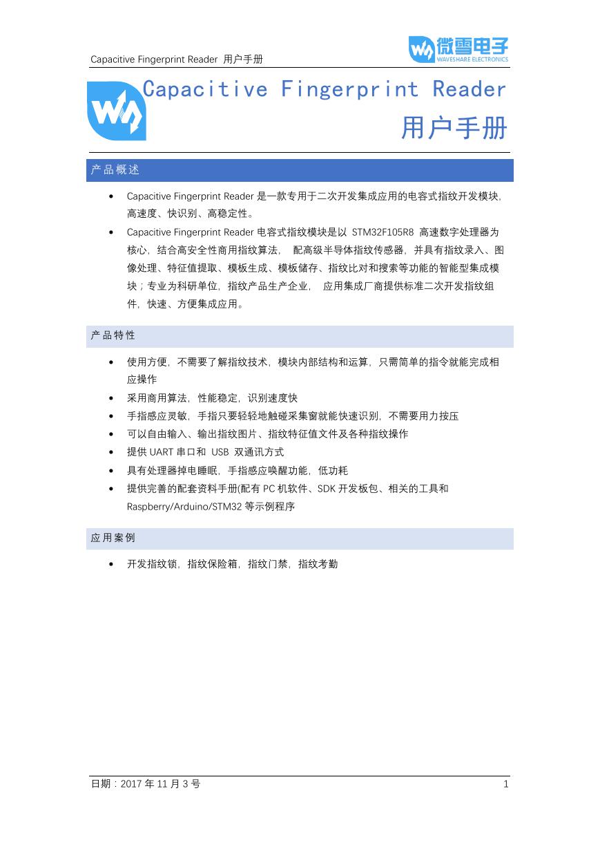 用户手册(Capacitive_Fingerprint_Reader_User_Manual_CN).pdf
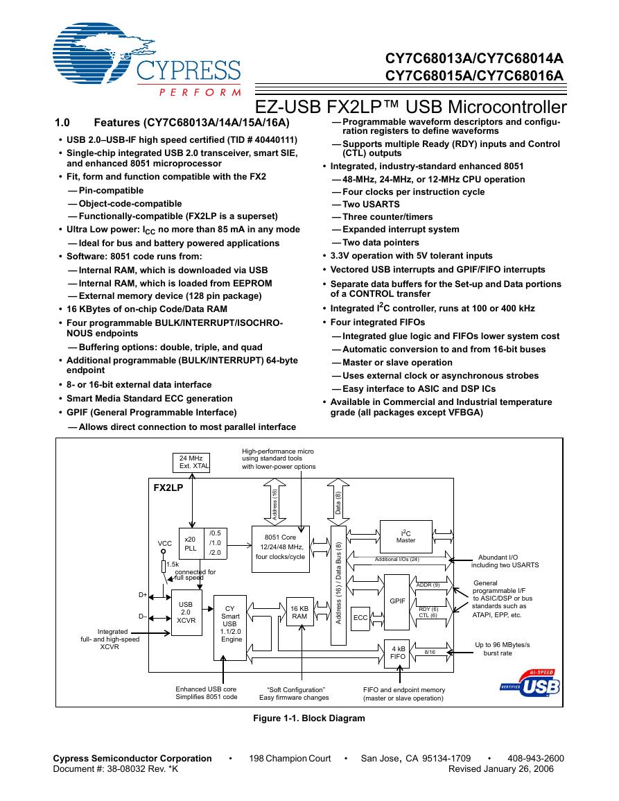 CY7C68013A(英文版)(CY7C68013A).pdf
 TechnicalReference_Dem.pdf