Freescale Semiconductor
Advance Information
3-Axis, Digital Magnetometer
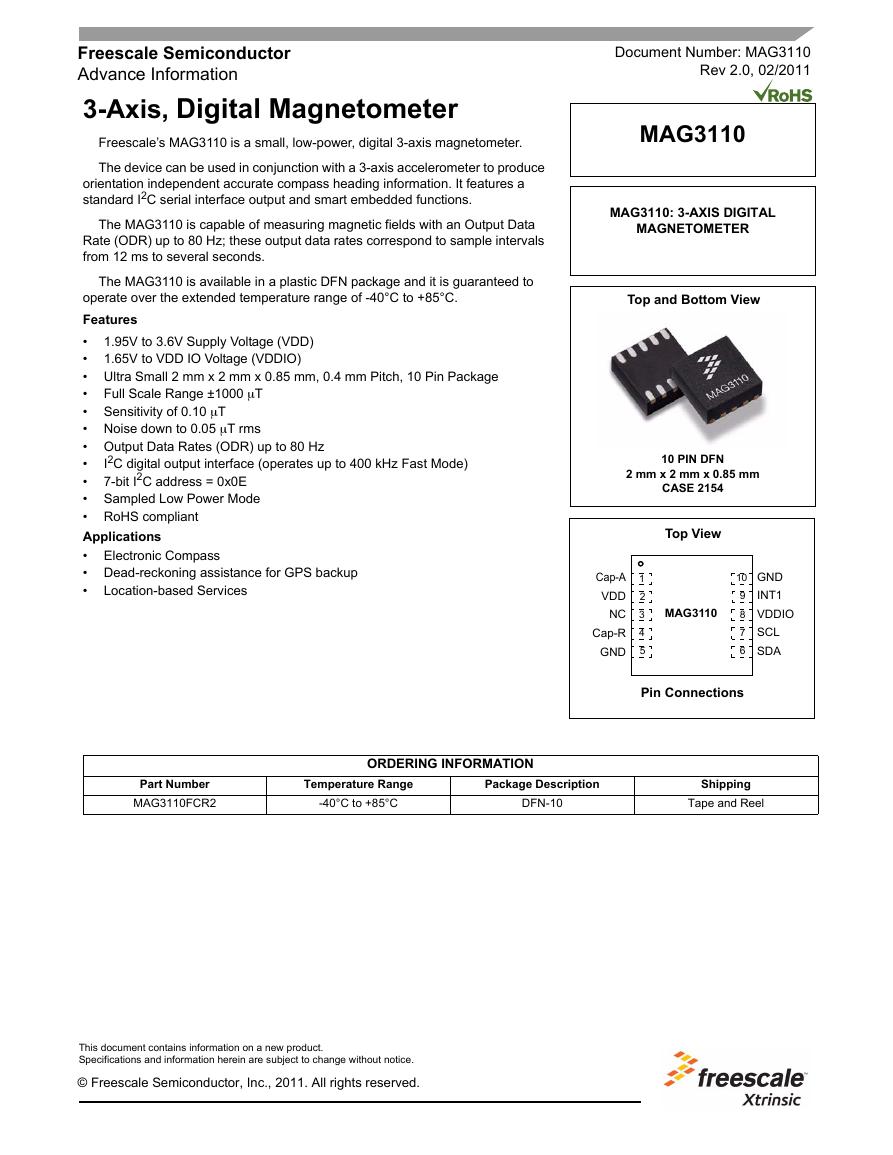
Freescale’s MAG3110 is a small, low-power, digital 3-axis magnetometer.
The device can be used in conjunction with a 3-axis accelerometer to produce
orientation independent accurate compass heading information. It features a
standard I2C serial interface output and smart embedded functions.
The MAG3110 is capable of measuring magnetic fields with an Output Data
Rate (ODR) up to 80 Hz; these output data rates correspond to sample intervals
from 12 ms to several seconds.
The MAG3110 is available in a plastic DFN package and it is guaranteed to
Full Scale Range ±1000 μT
1.95V to 3.6V Supply Voltage (VDD)
1.65V to VDD IO Voltage (VDDIO)
operate over the extended temperature range of -40°C to +85°C.
Features
•
•
• Ultra Small 2 mm x 2 mm x 0.85 mm, 0.4 mm Pitch, 10 Pin Package
•
• Sensitivity of 0.10 μT
• Noise down to 0.05 μT rms
• Output Data Rates (ODR) up to 80 Hz
•
•
• Sampled Low Power Mode
• RoHS compliant
Applications
• Electronic Compass
• Dead-reckoning assistance for GPS backup
•
I2C digital output interface (operates up to 400 kHz Fast Mode)
7-bit I2C address = 0x0E
Document Number: MAG3110
Rev 2.0, 02/2011
MAG3110
MAG3110: 3-AXIS DIGITAL
MAGNETOMETER
Top and Bottom View
2 mm x 2 mm x 0.85 mm
10 PIN DFN
CASE 2154
Top View
MAG3110
10
9
8
7
6
GND
INT1
VDDIO
SCL
SDA
Cap-A
VDD
NC
Cap-R
GND
1
2
3
4
5
Pin Connections
Location-based Services
Part Number
MAG3110FCR2
Temperature Range
-40°C to +85°C
Package Description
DFN-10
Shipping
Tape and Reel
ORDERING INFORMATION
This document contains information on a new product.
Specifications and information herein are subject to change without notice.
© Freescale Semiconductor, Inc., 2011. All rights reserved.
�
Application Notes for Reference
The following is a list of Freescale Application Notes written for the MAG3110:
• AN4246, Calibrating for Soft Iron and Hard Iron Distortions
• AN4247, PCB Layout Guidelines and Recommendations
• AN4248, Using the MAG3110 Magnetometer for an eCompass Application
• AN4249, Using the MAG3110 Magnetometer to Implement a 3-D Pointer
1
1.1
Block Diagram and Pin Description
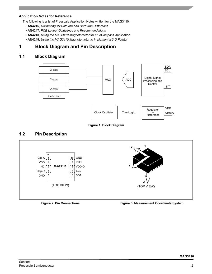
Block Diagram
X-axis
Y-axis
Z-axis
Self-Test
MUX
ADC
Digital Signal
Processing and
Control
SDA
SCL
INT1
Clock Oscillator
Trim Logic
Regulator
Reference
+
VDD
VDDIO
Figure 1. Block Diagram
1.2
Pin Description
Cap-A
VDD
NC
Cap-R
GND
1
2
3
4
5
MAG3110
(TOP VIEW)
10
9
8
7
6
GND
INT1
VDDIO
SCL
SDA
X
1
Y
Z
(TOP VIEW)
Figure 2. Pin Connections
Figure 3. Measurement Coordinate System
Sensors
Freescale Semiconductor
MAG3110
2
�
Table 1. Pin Description
Pin
1
2
3
4
5
6
7
8
9
10
Name
Cap-A
VDD
NC
Bypass Cap for Internal Regulator
Power Supply, 1.95V – 3.6V
No Connect – do not connect
Function
Cap-R
Cap for Reset Pulse
GND
SDA
SCL
GND
I2C Serial Data (Write = 0x1C; Read = 0x1D)
I2C Serial Clock
VDDIO
Power for I/O Buffers, 1.65V - VDD
INT1
GND
Interrupt - Active High Output
GND
1.3
Application Circuit
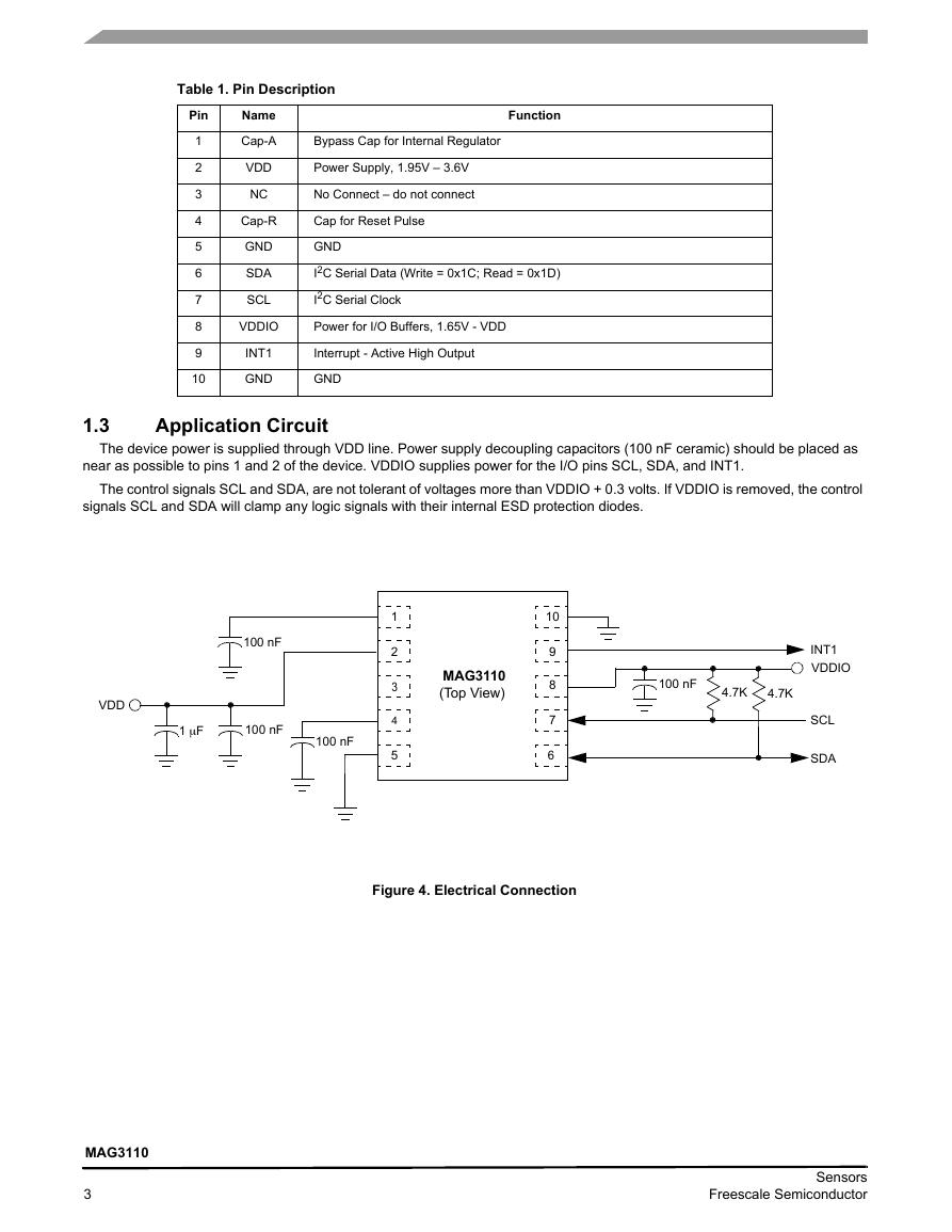
The device power is supplied through VDD line. Power supply decoupling capacitors (100 nF ceramic) should be placed as
near as possible to pins 1 and 2 of the device. VDDIO supplies power for the I/O pins SCL, SDA, and INT1.
The control signals SCL and SDA, are not tolerant of voltages more than VDDIO + 0.3 volts. If VDDIO is removed, the control
signals SCL and SDA will clamp any logic signals with their internal ESD protection diodes.
100 nF
VDD
1 μF
100 nF
100 nF
1
2
3
4
5
MAG3110
(Top View)
10
9
8
7
6
100 nF
4.7K
4.7K
INT1
VDDIO
SCL
SDA
Figure 4. Electrical Connection
MAG3110
3
Sensors
Freescale Semiconductor
�
Operating and Electrical Specifications
Operating Characteristics
2
2.1
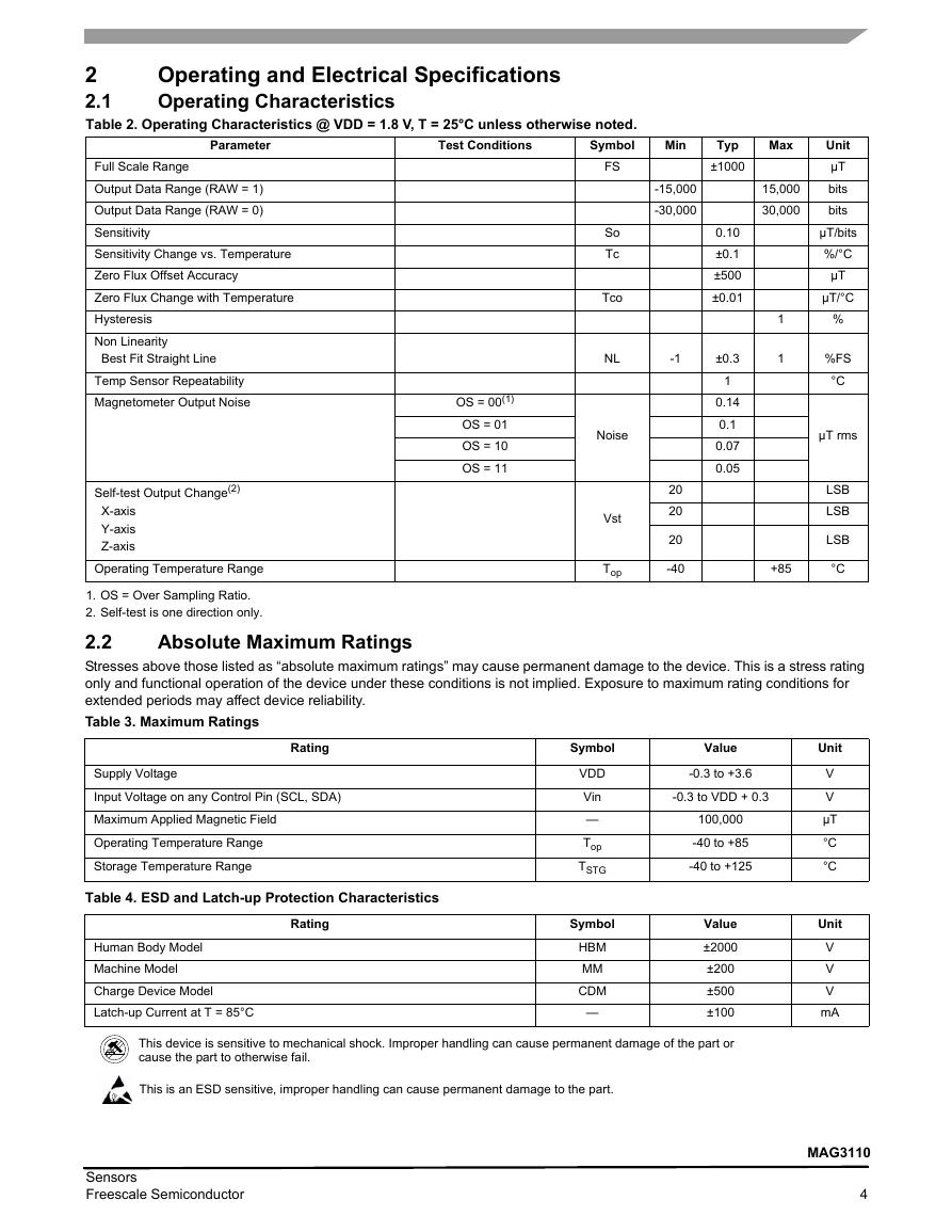
Table 2. Operating Characteristics @ VDD = 1.8 V, T = 25°C unless otherwise noted.
Symbol
Parameter
Test Conditions
Full Scale Range
Output Data Range (RAW = 1)
Output Data Range (RAW = 0)
Sensitivity
Sensitivity Change vs. Temperature
Zero Flux Offset Accuracy
Zero Flux Change with Temperature
Hysteresis
Non Linearity
Best Fit Straight Line
Temp Sensor Repeatability
Magnetometer Output Noise
Self-test Output Change(2)
X-axis
Y-axis
Z-axis
Operating Temperature Range
Min
Typ
±1000
-15,000
-30,000
Max
15,000
30,000
FS
So
Tc
Tco
OS = 00(1)
OS = 01
OS = 10
OS = 11
NL
-1
Noise
Vst
Top
20
20
20
-40
Unit
µT
bits
bits
µT/bits
%/°C
µT
µT/°C
%
%FS
°C
µT rms
LSB
LSB
LSB
°C
0.10
±0.1
±500
±0.01
±0.3
1
0.14
0.1
0.07
0.05
1
1
+85
Absolute Maximum Ratings
1. OS = Over Sampling Ratio.
2. Self-test is one direction only.
2.2
Stresses above those listed as “absolute maximum ratings” may cause permanent damage to the device. This is a stress rating
only and functional operation of the device under these conditions is not implied. Exposure to maximum rating conditions for
extended periods may affect device reliability.
Table 3. Maximum Ratings
Rating
Supply Voltage
Input Voltage on any Control Pin (SCL, SDA)
Maximum Applied Magnetic Field
Operating Temperature Range
Storage Temperature Range
Table 4. ESD and Latch-up Protection Characteristics
Rating
Human Body Model
Machine Model
Charge Device Model
Latch-up Current at T = 85°C
Symbol
VDD
Vin
—
Top
TSTG
Symbol
HBM
MM
CDM
—
Value
-0.3 to +3.6
-0.3 to VDD + 0.3
100,000
-40 to +85
-40 to +125
Value
±2000
±200
±500
±100
Unit
V
V
µT
°C
°C
Unit
V
V
V
mA
This device is sensitive to mechanical shock. Improper handling can cause permanent damage of the part or
cause the part to otherwise fail.
This is an ESD sensitive, improper handling can cause permanent damage to the part.
Sensors
Freescale Semiconductor
MAG3110
4
�
2.3
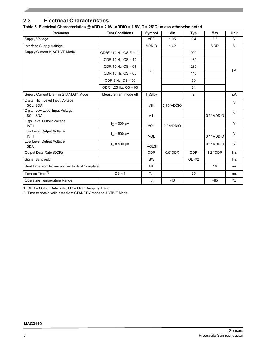
Table 5. Electrical Characteristics @ VDD = 2.0V, VDDIO = 1.8V, T = 25°C unless otherwise noted
Electrical Characteristics
Parameter
Test Conditions
Supply Voltage
Interface Supply Voltage
Supply Current in ACTIVE Mode
Supply Current Drain in STANDBY Mode
Digital High Level Input Voltage
SCL, SDA
Digital Low Level Input Voltage
SCL, SDA
High Level Output Voltage
INT1
Low Level Output Voltage
INT1
Low Level Output Voltage
SDA
Output Data Rate (ODR)
Signal Bandwidth
Boot Time from Power applied to Boot Complete
Turn-on Time(2)
Operating Temperature Range
ODR(1) 10 Hz, OS(1) = 11
ODR 10 Hz, OS = 10
ODR 10 Hz, OS = 01
ODR 10 Hz, OS = 00
ODR 5 Hz, OS = 00
ODR 1.25 Hz, OS = 00
Measurement mode off
IO = 500 µA
IO = 500 µA
IO = 500 µA
OS = 1
1. ODR = Output Data Rate; OS = Over Sampling Ratio.
2. Time to obtain valid data from STANDBY mode to ACTIVE Mode.
Typ
2.4
900
480
280
140
70
24
2
Symbol
VDD
VDDIO
Min
1.95
1.62
Idd
IddStby
VIH
VIL
0.75*VDDIO
VOH
0.9*VDDIO
VOL
VOLS
ODR
BW
BT
Ton
Top
0.8*ODR
-40
ODR
ODR/2
25
Max
3.6
VDD
Unit
V
V
µA
µA
V
V
V
V
V
Hz
Hz
ms
ms
°C
0.3* VDDIO
0.1* VDDIO
0.1* VDDIO
1.2 *ODR
10
+85
MAG3110
5
Sensors
Freescale Semiconductor
�
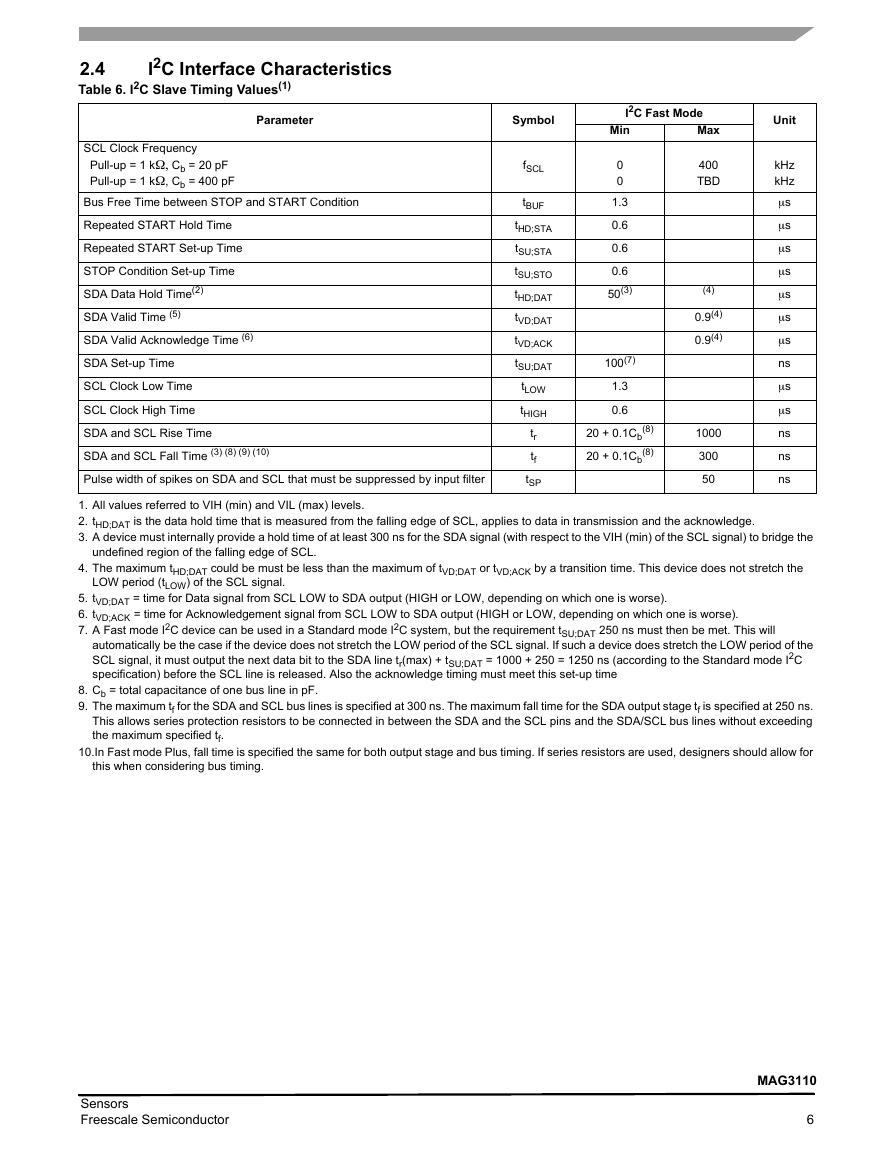
2.4
Table 6. I2C Slave Timing Values(1)
I2C Interface Characteristics
Parameter
SCL Clock Frequency
Pull-up = 1 kΩ, Cb = 20 pF
Pull-up = 1 kΩ, Cb = 400 pF
Bus Free Time between STOP and START Condition
Repeated START Hold Time
Repeated START Set-up Time
STOP Condition Set-up Time
SDA Data Hold Time(2)
SDA Valid Time (5)
SDA Valid Acknowledge Time (6)
SDA Set-up Time
SCL Clock Low Time
SCL Clock High Time
SDA and SCL Rise Time
SDA and SCL Fall Time (3) (8) (9) (10)
Pulse width of spikes on SDA and SCL that must be suppressed by input filter
Symbol
fSCL
tBUF
tHD;STA
tSU;STA
tSU;STO
tHD;DAT
tVD;DAT
tVD;ACK
tSU;DAT
tLOW
tHIGH
tr
tf
tSP
I2C Fast Mode
Min
0
0
1.3
0.6
0.6
0.6
50(3)
100(7)
1.3
0.6
20 + 0.1Cb
20 + 0.1Cb
(8)
(8)
Max
400
TBD
(4)
0.9(4)
0.9(4)
1000
300
50
Unit
kHz
kHz
μs
μs
μs
μs
μs
μs
μs
ns
μs
μs
ns
ns
ns
1. All values referred to VIH (min) and VIL (max) levels.
2. tHD;DAT is the data hold time that is measured from the falling edge of SCL, applies to data in transmission and the acknowledge.
3. A device must internally provide a hold time of at least 300 ns for the SDA signal (with respect to the VIH (min) of the SCL signal) to bridge the
undefined region of the falling edge of SCL.
4. The maximum tHD;DAT could be must be less than the maximum of tVD;DAT or tVD;ACK by a transition time. This device does not stretch the
LOW period (tLOW) of the SCL signal.
5. tVD;DAT = time for Data signal from SCL LOW to SDA output (HIGH or LOW, depending on which one is worse).
6. tVD;ACK = time for Acknowledgement signal from SCL LOW to SDA output (HIGH or LOW, depending on which one is worse).
7. A Fast mode I2C device can be used in a Standard mode I2C system, but the requirement tSU;DAT 250 ns must then be met. This will
automatically be the case if the device does not stretch the LOW period of the SCL signal. If such a device does stretch the LOW period of the
SCL signal, it must output the next data bit to the SDA line tr(max) + tSU;DAT = 1000 + 250 = 1250 ns (according to the Standard mode I2C
specification) before the SCL line is released. Also the acknowledge timing must meet this set-up time
8. Cb = total capacitance of one bus line in pF.
9. The maximum tf for the SDA and SCL bus lines is specified at 300 ns. The maximum fall time for the SDA output stage tf is specified at 250 ns.
This allows series protection resistors to be connected in between the SDA and the SCL pins and the SDA/SCL bus lines without exceeding
the maximum specified tf.
10.In Fast mode Plus, fall time is specified the same for both output stage and bus timing. If series resistors are used, designers should allow for
this when considering bus timing.
Sensors
Freescale Semiconductor
MAG3110
6
�
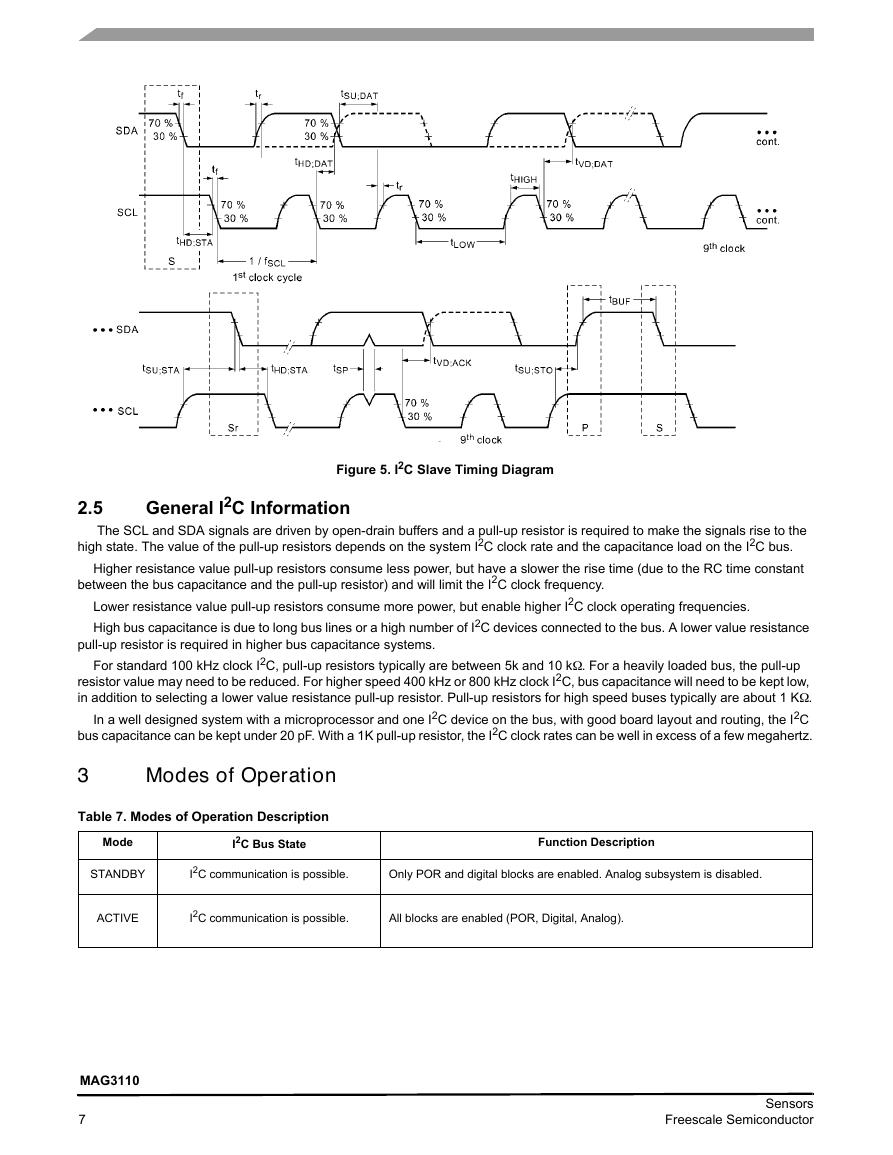
Figure 5. I2C Slave Timing Diagram
2.5
General I2C Information
The SCL and SDA signals are driven by open-drain buffers and a pull-up resistor is required to make the signals rise to the
high state. The value of the pull-up resistors depends on the system I2C clock rate and the capacitance load on the I2C bus.
Higher resistance value pull-up resistors consume less power, but have a slower the rise time (due to the RC time constant
between the bus capacitance and the pull-up resistor) and will limit the I2C clock frequency.
Lower resistance value pull-up resistors consume more power, but enable higher I2C clock operating frequencies.
High bus capacitance is due to long bus lines or a high number of I2C devices connected to the bus. A lower value resistance
pull-up resistor is required in higher bus capacitance systems.
For standard 100 kHz clock I2C, pull-up resistors typically are between 5k and 10 kΩ. For a heavily loaded bus, the pull-up
resistor value may need to be reduced. For higher speed 400 kHz or 800 kHz clock I2C, bus capacitance will need to be kept low,
in addition to selecting a lower value resistance pull-up resistor. Pull-up resistors for high speed buses typically are about 1 KΩ.
In a well designed system with a microprocessor and one I2C device on the bus, with good board layout and routing, the I2C
bus capacitance can be kept under 20 pF. With a 1K pull-up resistor, the I2C clock rates can be well in excess of a few megahertz.
3
Modes of Operation
Table 7. Modes of Operation Description
Mode
I2C Bus State
Function Description
STANDBY
I2C communication is possible.
Only POR and digital blocks are enabled. Analog subsystem is disabled.
ACTIVE
I2C communication is possible.
All blocks are enabled (POR, Digital, Analog).
MAG3110
7
Sensors
Freescale Semiconductor
�
4
Functionality
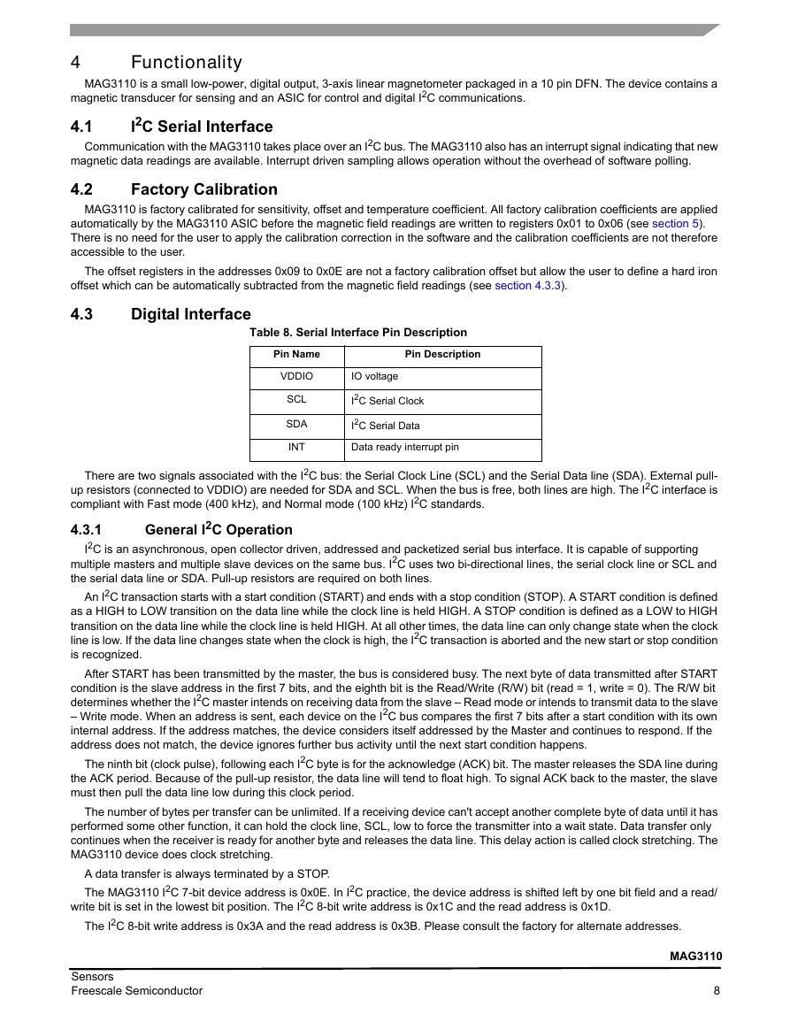
MAG3110 is a small low-power, digital output, 3-axis linear magnetometer packaged in a 10 pin DFN. The device contains a
magnetic transducer for sensing and an ASIC for control and digital I2C communications.
4.1
I2C Serial Interface
Communication with the MAG3110 takes place over an I2C bus. The MAG3110 also has an interrupt signal indicating that new
magnetic data readings are available. Interrupt driven sampling allows operation without the overhead of software polling.
4.2
Factory Calibration
MAG3110 is factory calibrated for sensitivity, offset and temperature coefficient. All factory calibration coefficients are applied
automatically by the MAG3110 ASIC before the magnetic field readings are written to registers 0x01 to 0x06 (see section 5).
There is no need for the user to apply the calibration correction in the software and the calibration coefficients are not therefore
accessible to the user.
The offset registers in the addresses 0x09 to 0x0E are not a factory calibration offset but allow the user to define a hard iron
offset which can be automatically subtracted from the magnetic field readings (see section 4.3.3).
4.3
Digital Interface
Table 8. Serial Interface Pin Description
Pin Name
Pin Description
VDDIO
IO voltage
SCL
SDA
INT
I2C Serial Clock
I2C Serial Data
Data ready interrupt pin
There are two signals associated with the I2C bus: the Serial Clock Line (SCL) and the Serial Data line (SDA). External pull-
up resistors (connected to VDDIO) are needed for SDA and SCL. When the bus is free, both lines are high. The I2C interface is
compliant with Fast mode (400 kHz), and Normal mode (100 kHz) I2C standards.
4.3.1
General I2C Operation
I2C is an asynchronous, open collector driven, addressed and packetized serial bus interface. It is capable of supporting
multiple masters and multiple slave devices on the same bus. I2C uses two bi-directional lines, the serial clock line or SCL and
the serial data line or SDA. Pull-up resistors are required on both lines.
An I2C transaction starts with a start condition (START) and ends with a stop condition (STOP). A START condition is defined
as a HIGH to LOW transition on the data line while the clock line is held HIGH. A STOP condition is defined as a LOW to HIGH
transition on the data line while the clock line is held HIGH. At all other times, the data line can only change state when the clock
line is low. If the data line changes state when the clock is high, the I2C transaction is aborted and the new start or stop condition
is recognized.
After START has been transmitted by the master, the bus is considered busy. The next byte of data transmitted after START
condition is the slave address in the first 7 bits, and the eighth bit is the Read/Write (R/W) bit (read = 1, write = 0). The R/W bit
determines whether the I2C master intends on receiving data from the slave – Read mode or intends to transmit data to the slave
– Write mode. When an address is sent, each device on the I2C bus compares the first 7 bits after a start condition with its own
internal address. If the address matches, the device considers itself addressed by the Master and continues to respond. If the
address does not match, the device ignores further bus activity until the next start condition happens.
The ninth bit (clock pulse), following each I2C byte is for the acknowledge (ACK) bit. The master releases the SDA line during
the ACK period. Because of the pull-up resistor, the data line will tend to float high. To signal ACK back to the master, the slave
must then pull the data line low during this clock period.
The number of bytes per transfer can be unlimited. If a receiving device can't accept another complete byte of data until it has
performed some other function, it can hold the clock line, SCL, low to force the transmitter into a wait state. Data transfer only
continues when the receiver is ready for another byte and releases the data line. This delay action is called clock stretching. The
MAG3110 device does clock stretching.
A data transfer is always terminated by a STOP.
The MAG3110 I2C 7-bit device address is 0x0E. In I2C practice, the device address is shifted left by one bit field and a read/
write bit is set in the lowest bit position. The I2C 8-bit write address is 0x1C and the read address is 0x1D.
The I2C 8-bit write address is 0x3A and the read address is 0x3B. Please consult the factory for alternate addresses.
Sensors
Freescale Semiconductor
MAG3110
8
�


 V2版本原理图(Capacitive-Fingerprint-Reader-Schematic_V2).pdf
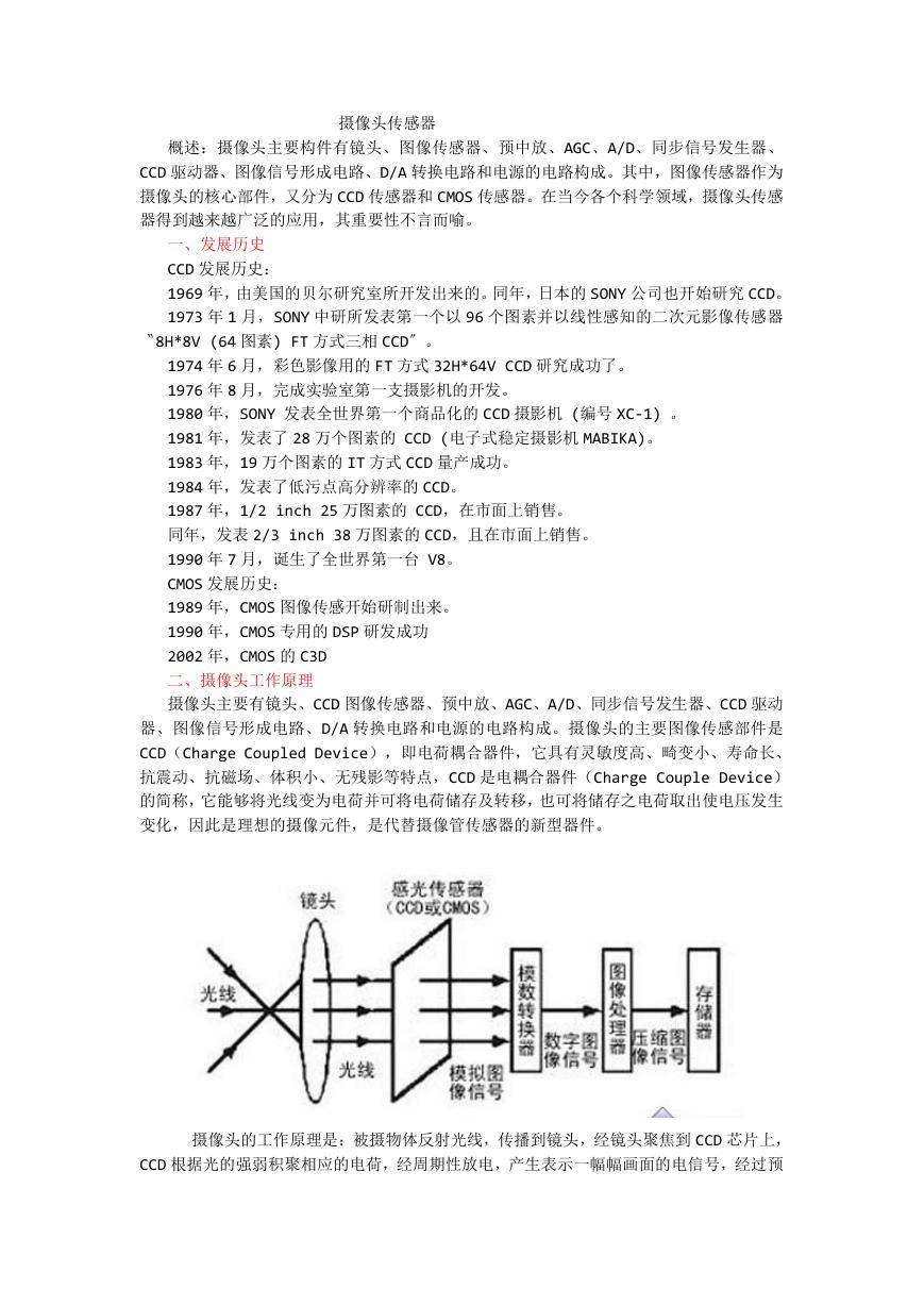 摄像头工作原理.doc
 VL53L0X简要说明(En.FLVL53L00216).pdf
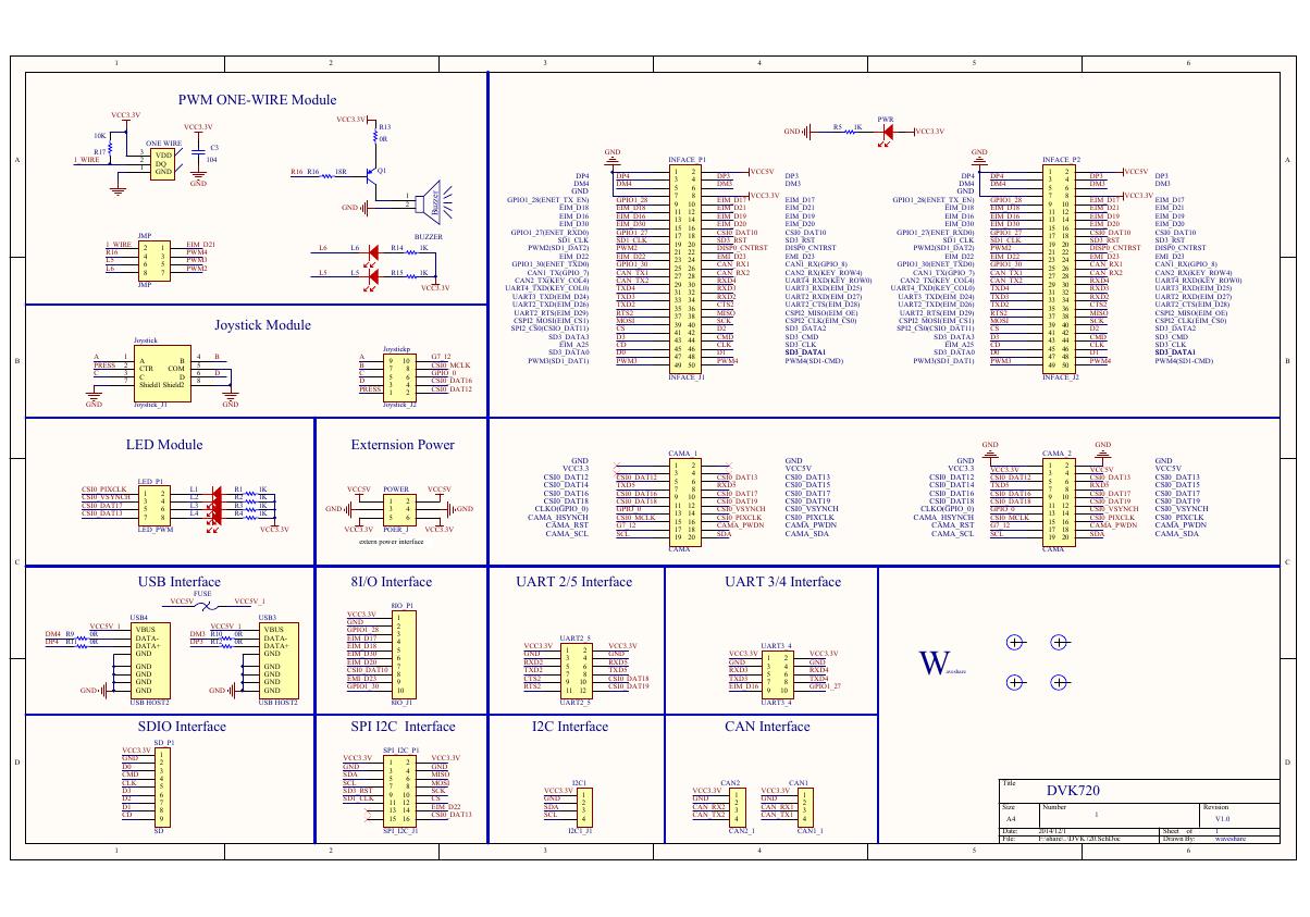 原理图(DVK720-Schematic).pdf
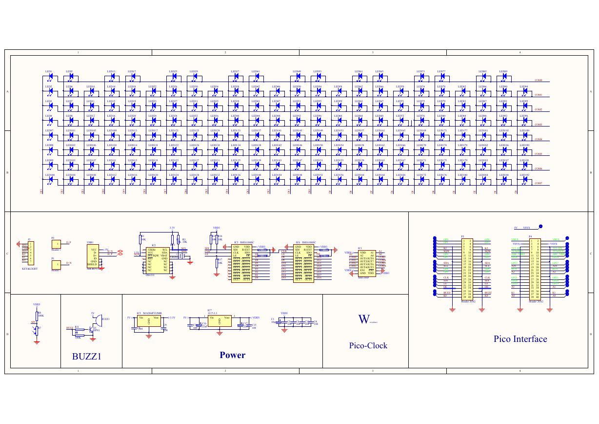 原理图(Pico-Clock-Green-Schdoc).pdf
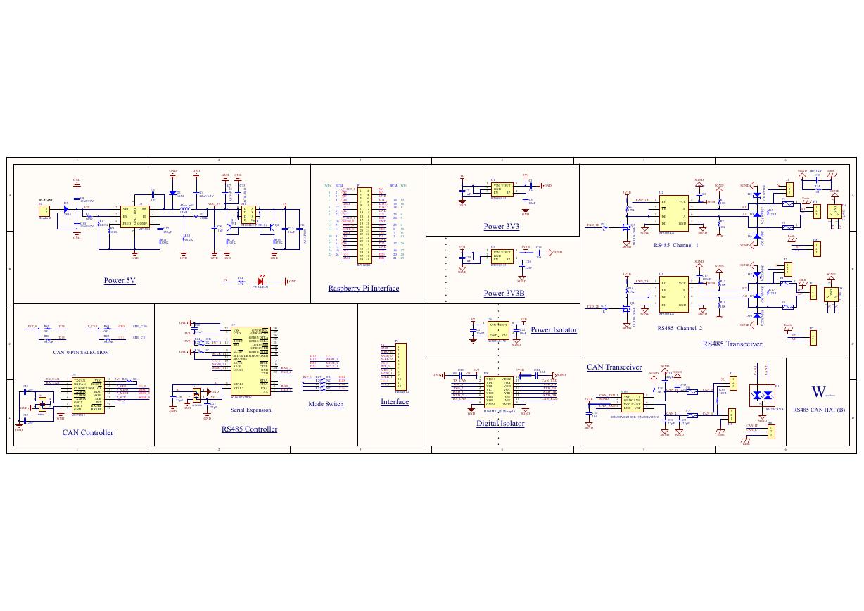 原理图(RS485-CAN-HAT-B-schematic).pdf
 File:SIM7500_SIM7600_SIM7800 Series_SSL_Application Note_V2.00.pdf
 ADS1263(Ads1262).pdf
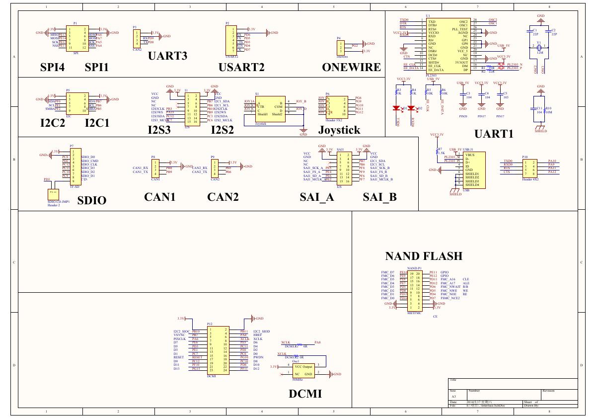 原理图(Open429Z-D-Schematic).pdf
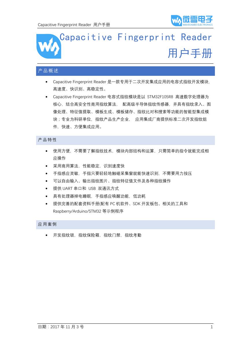 用户手册(Capacitive_Fingerprint_Reader_User_Manual_CN).pdf
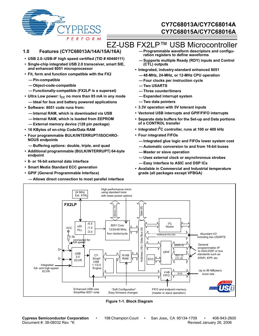 CY7C68013A(英文版)(CY7C68013A).pdf
 TechnicalReference_Dem.pdf