®
SP3222E/3232E
True +3.0V to +5.5V RS-232 Transceivers
FEATURES
■ Meets true EIA/TIA-232-F Standards
from a +3.0V to +5.5V power supply
■ Minimum 120Kbps Data Rate Under Full
Load
■ 1µA Low-Power Shutdown with Receivers
Active (SP3222E)
■ Interoperable with RS-232 down to +2.7V
power source
■ Enhanced ESD Specifications:
±15kV Human Body Model
±15kV IEC1000-4-2 Air Discharge
±8kV IEC1000-4-2 Contact Discharge
EN
C1+
V+
C1-
C2+
C2-
V-
T2OUT
R2IN
1
2
3
4
5
6
7
8
9
18
17
16
15
14
13
12
11
10
SHDN
VCC
GND
T1OUT
R1IN
R1OUT
T1IN
T2IN
R2OUT
SP3222E
DIP/SO
Now Available in Lead Free Packaging
Note: See page 6 for other pinouts
DESCRIPTION
The SP3222E/3232E series is an RS-232 transceiver solution intended for portable or hand-
held applications such as notebook or palmtop computers. The SP3222E/3232E series has
a high-efficiency, charge-pump power supply that requires only 0.1µF capacitors in 3.3V
operation. This charge pump allows the SP3222E/3232E series to deliver true RS-232
performance from a single power supply ranging from +3.3V to +5.0V. The SP3222E/3232E
are 2-driver/2-receiver devices. This series is ideal for portable or hand-held applications such
as notebook or palmtop computers. The ESD tolerance of the SP3222E/3232E devices are
over ±15kV for both Human Body Model and IEC1000-4-2 Air discharge test methods. The
SP3222E device has a low-power shutdown mode where the devices' driver outputs and
charge pumps are disabled. During shutdown, the supply current falls to less than 1µA.
SELECTION TABLE
LEDOM
seilppuSrewoP
232-SR
srevirD
srevirD
srevirD
srevirD
srevirD
232-SR
lanretxE
srevieceR
srevieceR
srevieceR
srevieceR
srevieceR
stnenopmoC
stnenopmoC
stnenopmoC
stnenopmoC
stnenopmoC
nwodtuhS
2223PS
V5.5+otV0.3+
2323PS
V5.5+otV0.3+
2
2
2
2
4
4
seY
oN
LTT
etatS-3
etatS-3
etatS-3
etatS-3
etatS-3
seY
oN
fo.oN
sniP sniP sniP sniP sniP
02,81
61
Date: 02/24/05 SP3222E, SP3232E True +3.0 to +5.0V RS-232 Transceivers
© Copyright 2005 Sipex Corporation
1
�
ABSOLUTE MAXIMUM RATINGS
These are stress ratings only and functional operation of the
device at these ratings or any other above those indicated in
the operation sections of the specifications below is not
implied. Exposure to absolute maximum rating conditions
for extended periods of time may affect reliability and cause
permanent damage to the device.
VCC................................................................-0.3V to +6.0V
V+ (NOTE 1)................................................-0.3V to +7.0V
V- (NOTE 1)................................................+0.3V to -7.0V
V+ + |V-| (NOTE 1)....................................................+13V
ICC (DC VCC or GND current).................................±100mA
Input Voltages
TxIN, EN ................................................... -0.3V to +6.0V
RxIN .......................................................................... ±15V
Output Voltages
TxOUT ...................................................................... ±15V
RxOUT ........................................... -0.3V to (VCC + 0.3V)
Short-Circuit Duration
TxOUT ............................................................ Continuous
Storage Temperature .............................. -65°C to +150°C
Power Dissipation Per Package
20-pin SSOP (derate 9.25mW/oC above +70oC) ..... 750mW
18-pin PDIP (derate 15.2mW/oC above +70oC) .... 1220mW
18-pin SOIC (derate 15.7mW/oC above +70oC) ... 1260mW
20-pin TSSOP (derate 11.1mW/oC above +70oC) .. 890mW
16-pin SSOP (derate 9.69mW/oC above +70oC) ..... 775mW
16-pin PDIP (derate 14.3mW/oC above +70oC) .... 1150mW
16-pin Wide SOIC (derate 11.2mW/oC above +70oC) 900mW
16-pin TSSOP (derate 10.5mW/oC above +70oC) .. 850mW
16-pin nSOIC (derate 13.57mW/°C above +70°C) .. 1086mW
NOTE 1: V+ and V- can have maximum magnitudes of 7V, but their absolute difference cannot exceed 13V.
Unless otherwise noted, the following specifications apply for VCC = +3.0V to +5.0V with TAMB = TMIN to TMAX
RETEMARAP
.NIM
.PYT
.XAM
STINU
SNOITIDNOC
ELECTRICAL CHARACTERISTICS
SCITSIRETCARAHCCD
tnerruCylppuS
tnerruCylppuSnwodtuhS
3.0
0.1
STUPTUOREVIECERDNASTUPNICIGOL
WOLdlohserhTcigoLtupnI
HGIHdlohserhTcigoLtupnI
0.2
4.2
tnerruCegakaeLtupnI
tnerruCegakaeLtuptuO
WOLegatloVtuptuO
HGIHegatloVtuptuO
STUPTUOREVIRD
10.0±
50.0±
V CC
6.0-
V CC
1.0-
gniwSegatloVtuptuO
0.5±
4.5±
0.1
01
8.0
0.1±
01±
4.0
ecnatsiseRtuptuO
003
tnerruCtiucriC-trohStuptuO
tnerruCegakaeLtuptuO
53±
07±
06±
001±
52±
Am
µA
V
V
µA
µA
V
V
V
Ω
Am
Am
µA
T,daolon
BMA
52+=
o V,C
V3.3=
CC
52+=
,DNG=NDHS
T BMA
o V,C
CC
V3.3+=
2etoN,NDHS,NE,NIxT
2etoN,V3.3=
2etoN,V0.5=
V CC
V CC
,NDHS,NE,NIxT
delbasidsreviecer
I
TUO
I
TUO
Am6.1=
Am0.1-=
T BMA
52+=
oC
k3 Ω
T BMA
,stuptuorevirdllatadnuorgotdaol
52+=
oC
T,V0=-V=+V=
TUO = + V2
V0=
V CC
V TUO
V TUO = + V51
V TUO = +
V,V21
delbasidsrevird,V5.5otV0=
CC
Date: 02/24/05 SP3222E, SP3232E True +3.0 to +5.0V RS-232 Transceivers
© Copyright 2005 Sipex Corporation
2
�
Unless otherwise noted, the following specifications apply for VCC = +3.0V to +5.0V with TAMB = TMIN to TMAX.
Typical Values apply at VCC = +3.3V or +5.0V and TAMB = 25oC.
RETEMARAP
.NIM
.PYT
.XAM
STINU
SNOITIDNOC
ELECTRICAL CHARACTERISTICS
STUPNIREVIECER
egnaRegatloVtupnI
WOLdlohserhTtupnI
HGIHdlohserhTtupnI
siseretsyHtupnI
ecnatsiseRtupnI
51-
6.0
8.0
3
2.1
5.1
5.1
8.1
3.0
5
51+
4.2
4.2
7
SCITSIRETCARAHCGNIMIT
etaRataDmumixaM
021
532
yaleDnoitagaporPrevirD
yaleDnoitagaporPrevieceR
emiTelbanEtuptuOrevieceR
emiTelbasiDtuptuOrevieceR
wekSrevirD
wekSrevieceR
etaRwelSnoigeR-noitisnarT
0.1
0.1
3.0
3.0
002
002
001
002
005
0001
03
V
V
V
V
kΩ
spbk
µs
µs
µs
sn
sn
sn
sn
/V µs
NOTE 2: Driver input hysteresis is typically 250mV.
V CC
V CC
V3.3=
V0.5=
V CC
V CC
V3.3=
V0.5=
k3= Ω C,
gnihctiwsrevirdeno,Fp0001=
L
RL
t
LHP R,
t HLP R,
L
L
K3= Ω C,
K3= Ω C,
L
L
Fp0001=
Fp0001=
LHP
t
t HLP
C,TUOxRotNIxR,
L
C,TUOxRotNIxR,
L
Fp051=
Fp051=
t|
t|
t-
HLP
T,|
BMA
52=
oC
LHP
t-
HLP
|
LHP
K3= Ω T,
L
R,V3.3=
V CC
V0.3+otV0.3-morfnekatstnemerusaem
V0.3-otV0.3+ro
52=
o
,C
BMA
Date: 02/24/05 SP3222E, SP3232E True +3.0 to +5.0V RS-232 Transceivers
© Copyright 2005 Sipex Corporation
3
�
Unless otherwise noted, the following performance characteristics apply for VCC = +3.3V, 120kbps data rates, all drivers
loaded with 3kΩ, 0.1µF charge pump capacitors, and TAMB = +25°C.
TYPICAL PERFORMANCE CHARACTERISTICS
]
V
[
e
g
a
t
l
o
V
t
u
p
t
u
O
r
e
t
t
i
m
s
n
a
r
T
6
4
2
0
-2
-4
-6
0
500
1000
1500
2000
Vout+
Vout-
Load Capacitance [pF]
]
s
µ
V
/
[
e
t
a
R
w
e
S
l
14
12
10
8
6
4
2
0
+Slew
-Slew
0
500
1000
1500
2000
2330
Load Capacitance [pF]
Figure 1. Transmitter Output Voltage VS. Load
Capacitance for the SP3222 and the SP3232
Figure 2. Slew Rate VS. Load Capacitance for the
SP3222 and the SP3232
118KHz
60KHz
10KHz
50
45
40
35
30
25
20
15
10
5
0
]
A
m
[
t
n
e
r
r
u
C
y
l
p
p
u
S
0
500
1000
1500
2000
2330
Load Capacitance [pF]
Figure 3. Supply Current VS. Load Capacitance when
Transmitting Data for the SP3222 and the SP3232
Date: 02/24/05 SP3222E, SP3232E True +3.0 to +5.0V RS-232 Transceivers
© Copyright 2005 Sipex Corporation
4
�
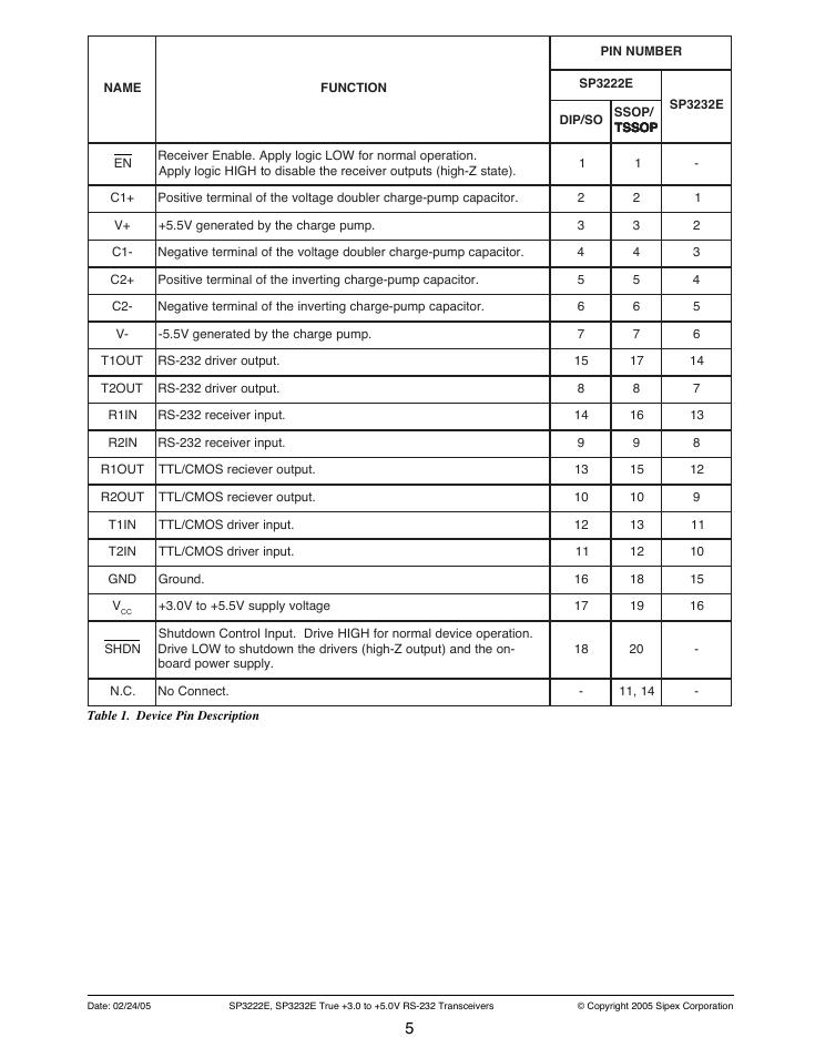
EMAN
NOITCNUF
NE
.noitarepolamronrofWOLcigolylppA.elbanErevieceR
.)etatsZ-hgih(stuptuoreviecerehtelbasidotHGIHcigolylppA
+1C
.roticapacpmup-egrahcrelbuodegatlovehtfolanimretevitisoP
+V
-1C
+2C
-2C
.pmupegrahcehtybdetarenegV5.5+
.roticapacpmup-egrahcrelbuodegatlovehtfolanimretevitageN
.roticapacpmup-egrahcgnitrevniehtfolanimretevitisoP
.roticapacpmup-egrahcgnitrevniehtfolanimretevitageN
-V
.pmupegrahcehtybdetarenegV5.5-
TUO1T
.tuptuorevird232-SR
TUO2T
.tuptuorevird232-SR
NI1R
.tupnireviecer232-SR
NI2R
.tupnireviecer232-SR
TUO1R
.tuptuoreveicerSOMC/LTT
TUO2R
.tuptuoreveicerSOMC/LTT
NI1T
.tupnirevirdSOMC/LTT
NI2T
.tupnirevirdSOMC/LTT
DNG
.dnuorG
V CC
egatlovylppusV5.5+otV0.3+
NDHS
.noitarepoecivedlamronrofHGIHevirD.tupnIlortnoCnwodtuhS
-noehtdna)tuptuoZ-hgih(srevirdehtnwodtuhsotWOLevirD
.ylppusrewopdraob
.C.N
.tcennoCoN
Table 1. Device Pin Description
-
41,11
REBMUNNIP
E2223PS
OS/PID
-/POSS
POSST
POSST
POSST
POSST
POSST
E2323PS
1
2
3
4
5
6
7
51
8
41
9
31
01
21
11
61
71
81
1
2
3
4
5
6
7
71
8
61
9
51
01
31
21
81
91
02
-
1
2
3
4
5
6
41
7
31
8
21
9
11
01
51
61
-
-
Date: 02/24/05 SP3222E, SP3232E True +3.0 to +5.0V RS-232 Transceivers
© Copyright 2005 Sipex Corporation
5
�
SP3222E
EN
C1+
V+
C1-
C2+
C2-
V-
T2OUT
R2IN
1
2
3
4
5
6
7
8
9
R2OUT
10
20
19
18
17
16
15
14
13
12
11
SHDN
VCC
GND
T1OUT
R1IN
R1OUT
N.C.
T1IN
T2IN
N.C.
EN
C1+
V+
C1-
C2+
C2-
V-
T2OUT
R2IN
1
2
3
4
5
6
7
8
9
18
17
16
15
14
13
12
11
10
SHDN
VCC
GND
T1OUT
R1IN
R1OUT
T1IN
T2IN
R2OUT
SP3222E
DIP/SO
SSOP/TSSOP
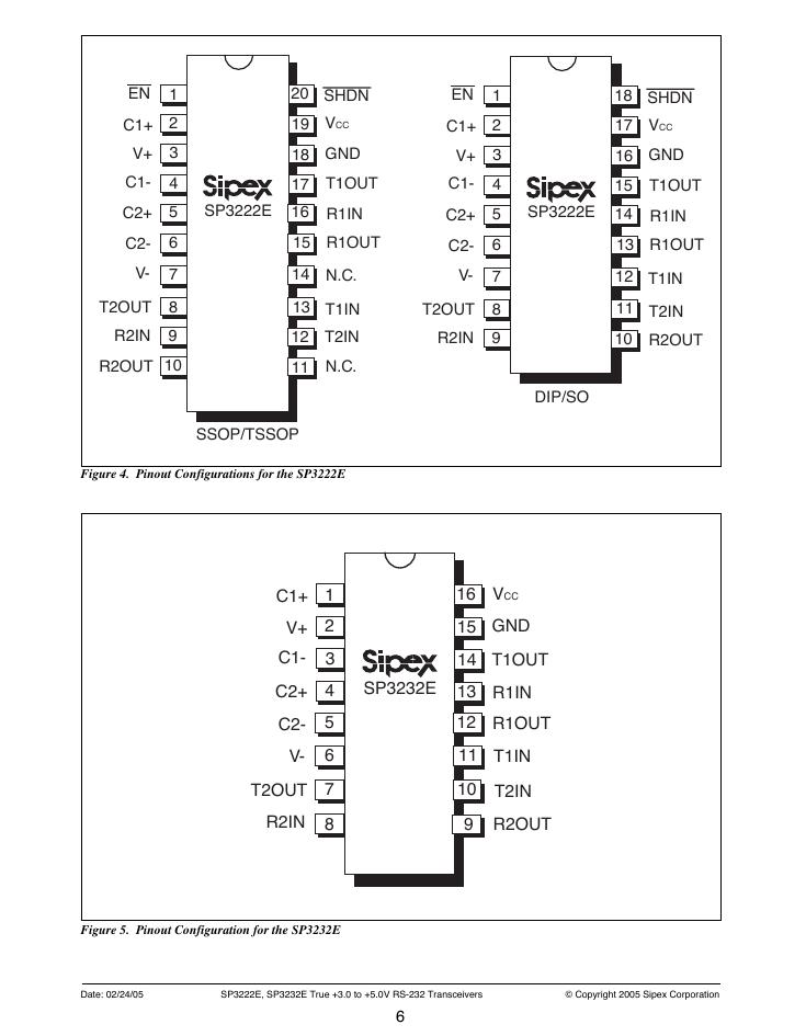
Figure 4. Pinout Configurations for the SP3222E
C1+
V+
C1-
C2+
C2-
V-
T2OUT
R2IN
1
2
3
4
5
6
7
8
SP3232E
16
15
14
13
12
11
10
VCC
GND
T1OUT
R1IN
R1OUT
T1IN
T2IN
9
R2OUT
Figure 5. Pinout Configuration for the SP3232E
Date: 02/24/05 SP3222E, SP3232E True +3.0 to +5.0V RS-232 Transceivers
© Copyright 2005 Sipex Corporation
6
�
C5
C1
C2
+
+
+
0.1µF
0.1µF
0.1µF
LOGIC
INPUTS
LOGIC
OUTPUTS
VCC
19
VCC
SP3222E
SSOP
TSSOP
2
C1+
4
5
C1-
C2+
6
C2-
13
T1IN
12
T2IN
3
V+
7
V-
+
0.1µF
*C3
C4
0.1µF
+
C5
C1
C2
+
+
+
0.1µF
0.1µF
0.1µF
T1OUT
17
T2OUT
8
RS-232
OUTPUTS
LOGIC
INPUTS
VCC
17
VCC
SP3222E
DIP/SO
2
C1+
4
5
C1-
C2+
6
C2-
12
T1IN
11
T2IN
3
V+
7
V-
+
0.1µF
*C3
C4
0.1µF
+
T1OUT
T2OUT
15
8
RS-232
OUTPUTS
15
R1OUT
R1IN
16
13
R1OUT
R1IN
14
10
R2OUT
1
EN
5kΩ
5kΩ
R2IN
9
SHDN
20
RS-232
INPUTS
LOGIC
OUTPUTS
GND
18
*can be returned to
either VCC or GND
10
R2OUT
1
EN
RS-232
INPUTS
5kΩ
5kΩ
R2IN
9
SHDN
18
GND
16
*can be returned to
either VCC or GND
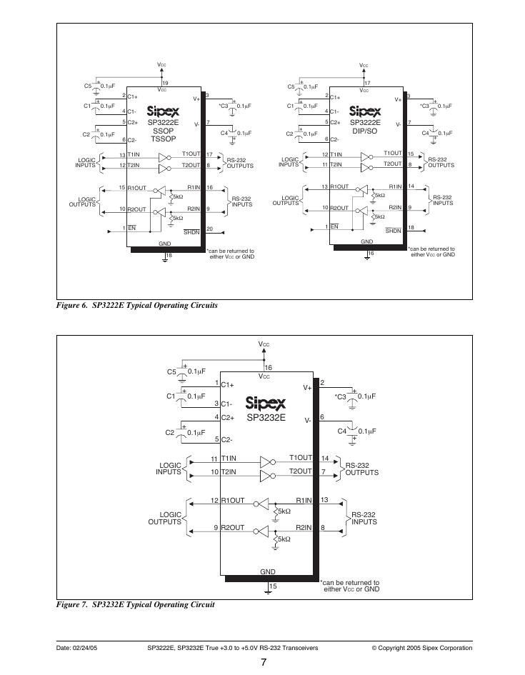
Figure 6. SP3222E Typical Operating Circuits
C5
C1
C2
+
+
+
0.1µF
0.1µF
0.1µF
LOGIC
INPUTS
LOGIC
OUTPUTS
VCC
16
VCC
SP3232E
1
C1+
3
4
C1-
C2+
5
C2-
11
T1IN
10
T2IN
2
6
V+
V-
+
0.1µF
*C3
C4
0.1µF
+
T1OUT
T2OUT
14
7
RS-232
OUTPUTS
12
R1OUT
R1IN
13
9
R2OUT
5kΩ
5kΩ
R2IN
8
RS-232
INPUTS
GND
15
*can be returned to
either VCC or GND
Figure 7. SP3232E Typical Operating Circuit
Date: 02/24/05 SP3222E, SP3232E True +3.0 to +5.0V RS-232 Transceivers
© Copyright 2005 Sipex Corporation
7
�
DESCRIPTION
The SP3222E/3232E transceivers meet the EIA/
TIA-232 and V.28/V.24 communication proto-
cols and can be implemented in battery-pow-
ered, portable, or hand-held applications such as
notebook or palmtop computers. The SP3222E/
3232E devices all feature Sipex's proprietary
on-board charge pump circuitry that generates 2
x VCC for RS-232 voltage levels from a single
+3.0V to +5.5V power supply. This series is
ideal for +3.3V-only systems, mixed +3.3V to
+5.5V systems, or +5.0V-only systems that re-
quire true RS-232 performance. The SP3222E/
3232E series have drivers that operate at a typi-
cal data rate of 235Kbps fully loaded.
The SP3222E and SP3232E are 2-driver/2-re-
ceiver devices ideal for portable or hand-held
applications. The SP3222E features a 1µA
shutdown mode that reduces power consump-
tion and extends battery life in portable systems.
Its receivers remain active in shutdown mode,
allowing external devices such as modems to be
monitored using only 1µA supply current.
THEORY OF OPERATION
The SP3222E/3232E series are made up of three
basic circuit blocks: 1. Drivers, 2. Receivers,
and 3. the Sipex proprietary charge pump.
Drivers
The drivers are inverting level transmitters that
convert TTL or CMOS logic levels to ±5.0V
EIA/TIA-232 levels inverted relative to the in-
put logic levels. Typically, the RS-232 output
voltage swing is ±5.5V with no load and at least
±5V minimum fully loaded. The driver outputs
are protected against infinite short-circuits to
ground without degradation in reliability. Driver
outputs will meet EIA/TIA-562 levels of ±3.7V
with supply voltages as low as 2.7V.
The drivers typically can operate at a data rate
of 235Kbps. The drivers can guarantee a data
rate of 120Kbps fully loaded with 3KΩ in
parallel with 1000pF, ensuring compatibility
with PC-to-PC communication software.
The slew rate of the driver output is internally
limited to a maximum of 30V/µs in order to meet
the EIA standards (EIA RS-232D 2.1.7, Para-
graph 5). The transition of the loaded output
from HIGH to LOW also meets the monotonic-
ity requirements of the standard.
The SP3222E/3232E drivers can maintain high
data rates up to 235Kbps fully loaded. Figure 8
shows a loopback test circuit used to test the
RS-232 drivers. Figure 9 shows the test results
of the loopback circuit with all drivers active at
120Kbps with RS-232 loads in parallel with
1000pF capacitors. Figure 10 shows the test
results where one driver was active at 235Kbps
and all drivers loaded with an RS-232 receiver
in parallel with a 1000pF capacitor. A solid
RS-232 data transmission rate of 120Kbps
provides compatibility with many designs
in personal computer peripherals and LAN
applications.
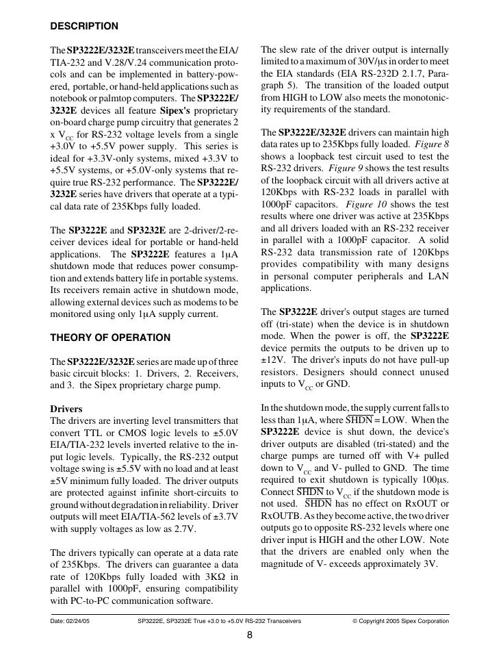
The SP3222E driver's output stages are turned
off (tri-state) when the device is in shutdown
mode. When the power is off, the SP3222E
device permits the outputs to be driven up to
±12V. The driver's inputs do not have pull-up
resistors. Designers should connect unused
inputs to VCC or GND.
In the shutdown mode, the supply current falls to
less than 1µA, where SHDN = LOW. When the
SP3222E device is shut down, the device's
driver outputs are disabled (tri-stated) and the
charge pumps are turned off with V+ pulled
down to VCC and V- pulled to GND. The time
required to exit shutdown is typically 100µs.
Connect SHDN to VCC if the shutdown mode is
not used. SHDN has no effect on RxOUT or
RxOUTB. As they become active, the two driver
outputs go to opposite RS-232 levels where one
driver input is HIGH and the other LOW. Note
that the drivers are enabled only when the
magnitude of V- exceeds approximately 3V.
Date: 02/24/05 SP3222E, SP3232E True +3.0 to +5.0V RS-232 Transceivers
© Copyright 2005 Sipex Corporation
8
�


 V2版本原理图(Capacitive-Fingerprint-Reader-Schematic_V2).pdf
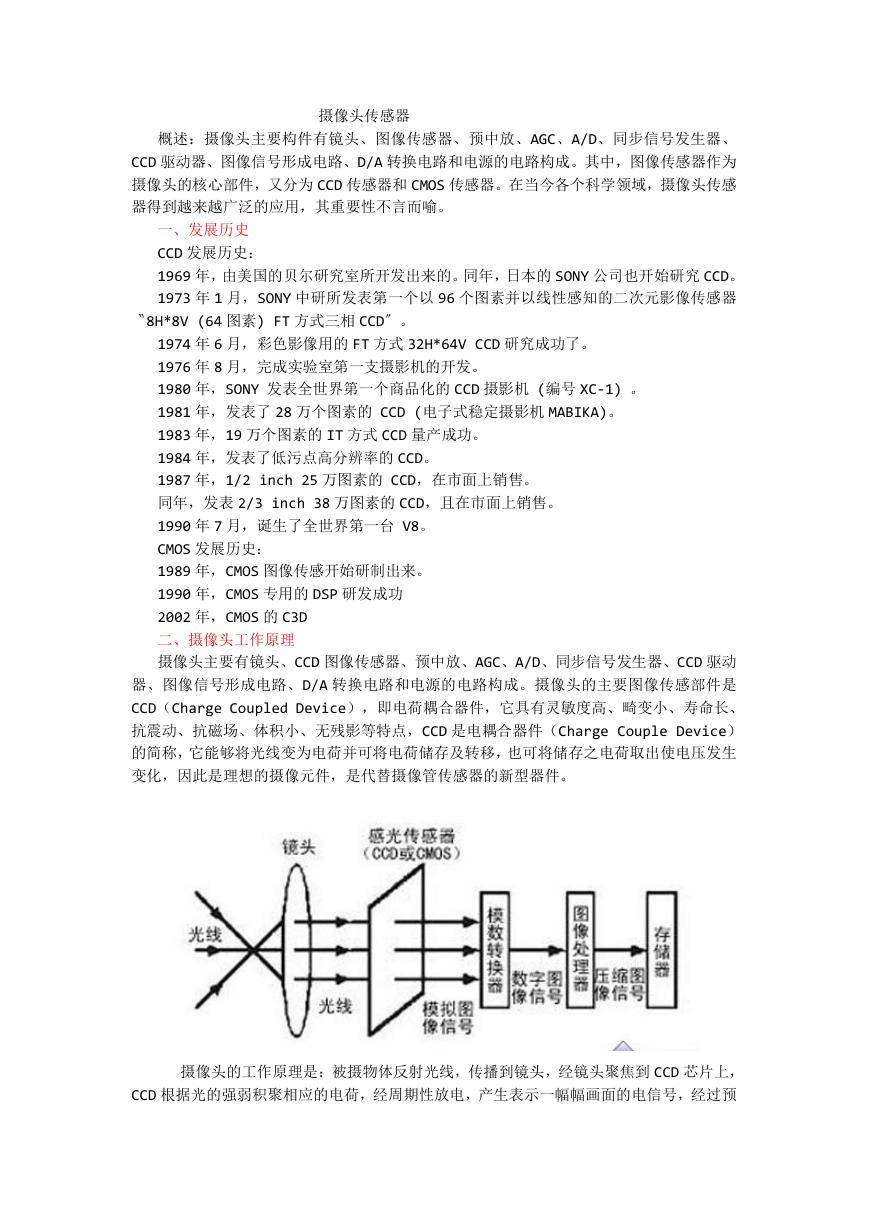 摄像头工作原理.doc
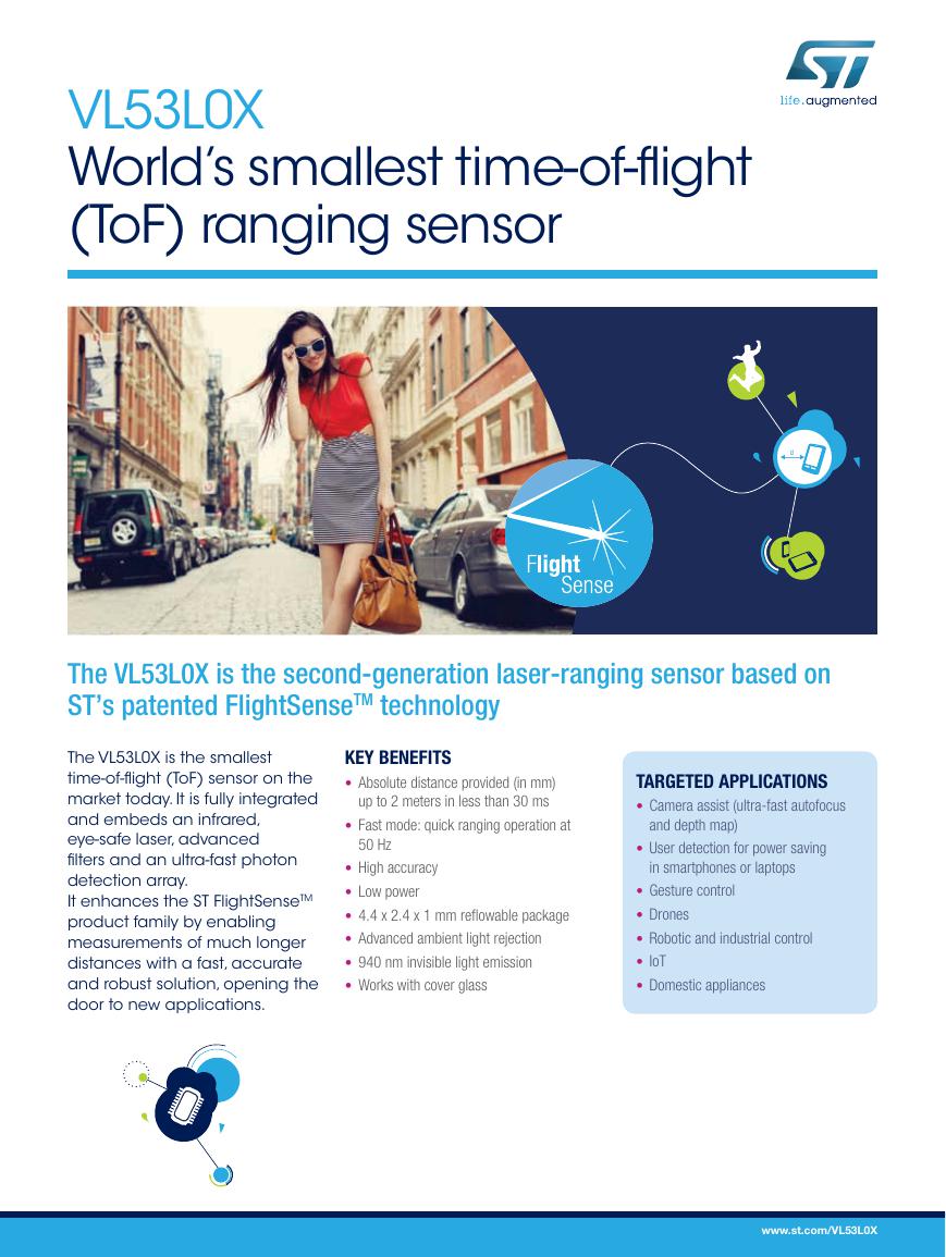 VL53L0X简要说明(En.FLVL53L00216).pdf
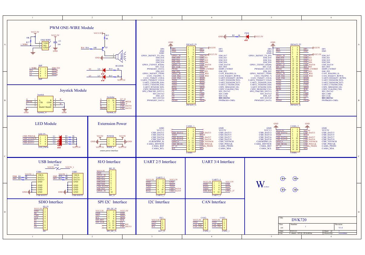 原理图(DVK720-Schematic).pdf
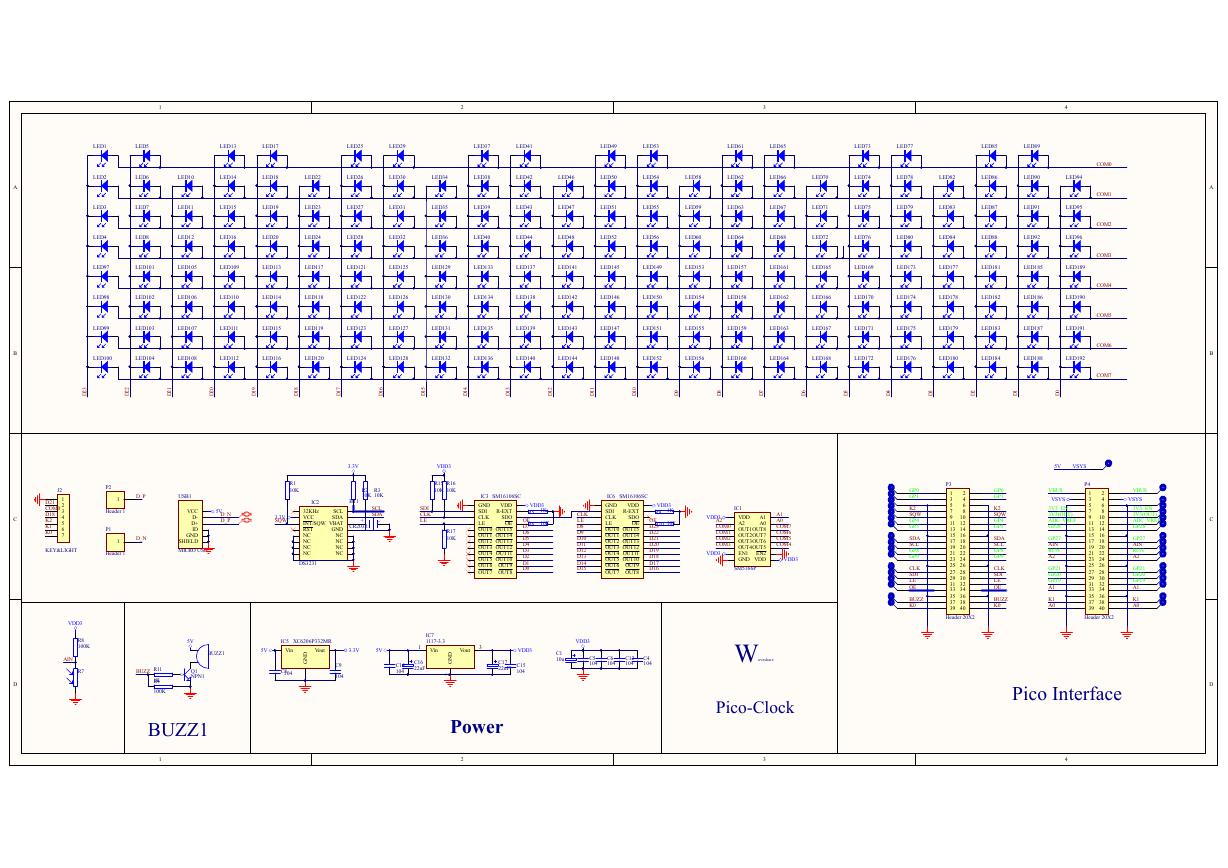 原理图(Pico-Clock-Green-Schdoc).pdf
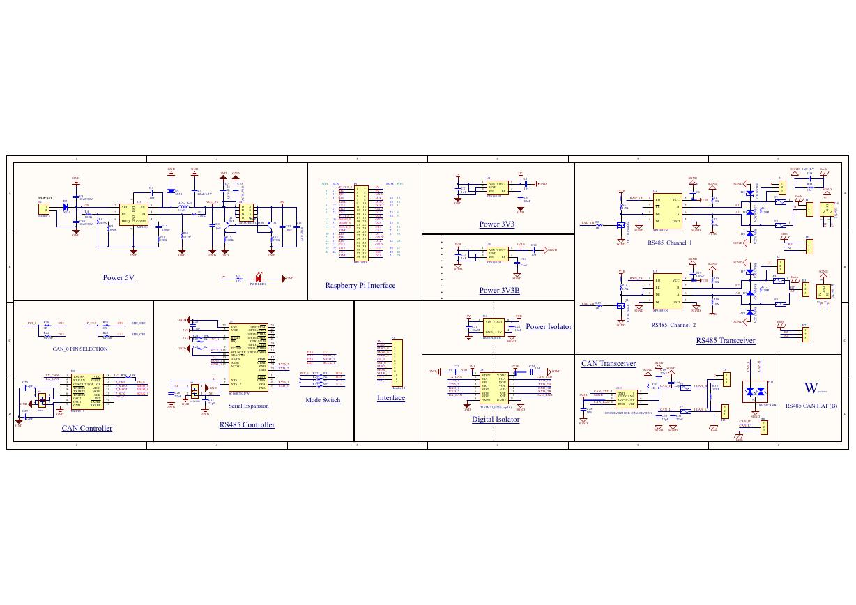 原理图(RS485-CAN-HAT-B-schematic).pdf
 File:SIM7500_SIM7600_SIM7800 Series_SSL_Application Note_V2.00.pdf
 ADS1263(Ads1262).pdf
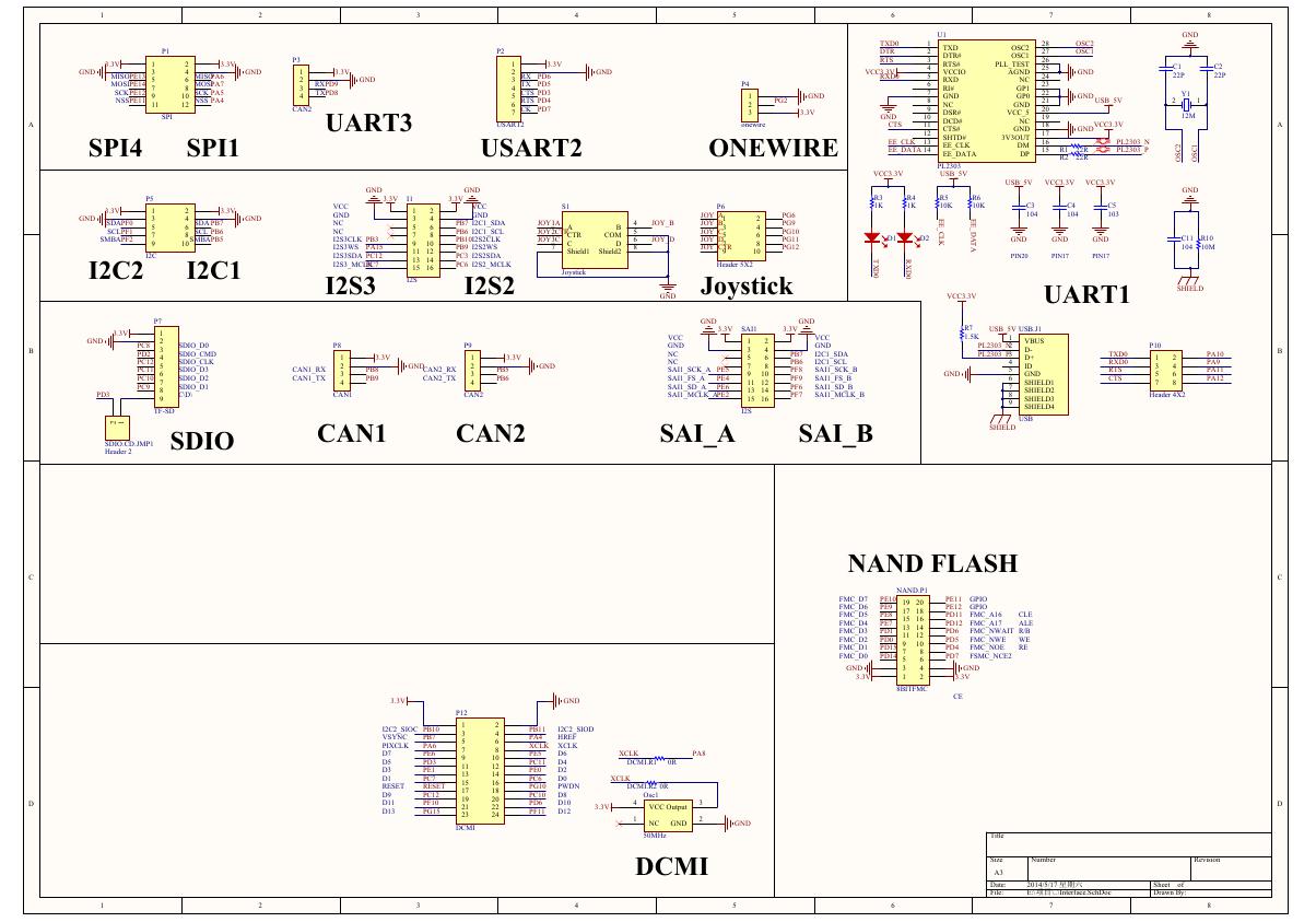 原理图(Open429Z-D-Schematic).pdf
 用户手册(Capacitive_Fingerprint_Reader_User_Manual_CN).pdf
 CY7C68013A(英文版)(CY7C68013A).pdf
 TechnicalReference_Dem.pdf