The Future of Analog IC Technology
DESCRIPTION
The MP3202 is a step-up converter designed for
driving up to 39 white LEDs (13 strings of 3 LEDs
each) from a 5V system rail. The MP3202 uses a
current mode, fixed frequency architecture to
regulate the LED current, which is measured
through an external current sense resistor. Its low
104mV feedback voltage reduces power loss and
improves efficiency. The OV pin monitors the
output voltage and turns off the converter if an
over-voltage condition is present due to an open
circuit condition.
The MP3202 includes under-voltage lockout,
current limiting and thermal overload protection
preventing damage in the event of an output
overload.
The MP3202 is available in small 6-pin TSOT23
or 8-pin QFN (2mm x 2mm) packages.
MP3202
1.3A Fixed Frequency
White LED Driver
FEATURES
• 2.5V to 6V Input Voltage Range
• On Board Power MOSFET
• Drives up to 39 White LEDs at 5V Input
• Up to 92% Efficiency
• Over 1MHz Fixed Switching Frequency
• Open Load Shutdown
• Low 104mV Feedback Voltage
• Soft-Start/PWM Dimming
• UVLO, Thermal Shutdown
•
Internal 1.3A Current Limit
• Available in TSOT23-6 and QFN8 Packages
APPLICATIONS
• Cell Phones
• Handheld Computers and PDAs
• Digital Still Cameras
• Small LCD Displays
“MPS” and “The Future of Analog IC Technology” are Registered Trademarks of
Monolithic Power Systems, Inc.
TYPICAL APPLICATION
VIN
4.5V - 6V
EN
IN
EN
MP3202
GND
SW
OV
FB
Efficiency vs
Input Voltage
IOUT=100mA
IOUT=180mA
100
90
80
70
60
13 Strings
)
%
(
I
Y
C
N
E
C
F
F
E
I
50
4.0
4.5
5.5
INPUT VOLTAGE (V)
5.0
6.0
MP3202 Rev. 0.9
9/13/2006
MPS Proprietary Information. Unauthorized Photocopy and Duplication Prohibited.
www.MonolithicPower.com
© 2006 MPS. All Rights Reserved.
1
�
MP3202 – 1.3A FIXED FREQUENCY WHITE LED DRIVER
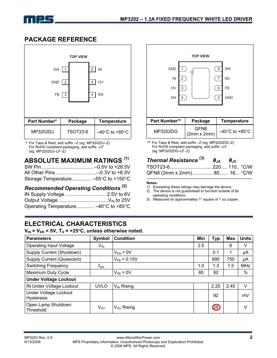
PACKAGE REFERENCE
TOP VIEW
SW
GND
FB
1
2
3
6
5
4
IN
OV
EN
TOP VIEW
GND
IN
OV
EN
1
2
3
4
8
7
6
5
SW
NC
FB
GND
Part Number*
Package
Temperature
Part Number**
MP3202DJ
TSOT23-6
–40°C to +85°C
MP3202DG
Package
QFN8
Temperature
(2mm x 2mm) –40°C to +85°C
* For Tape & Reel, add suffix –Z (eg. MP3202DJ–Z)
For RoHS compliant packaging, add suffix –LF
(eg. MP3202DJ–LF–Z)
ABSOLUTE MAXIMUM RATINGS (1)
SW Pin......................................–0.5V to +28.5V
All Other Pins..............................–0.3V to +6.5V
Storage Temperature.............. –55°C to +150°C
Recommended Operating Conditions (2)
IN Supply Voltage ..............................2.5V to 6V
Output Voltage....................................VIN to 25V
Operating Temperature............. –40°C to +85°C
** For Tape & Reel, add suffix –Z (eg. MP3202DG–Z)
For RoHS compliant packaging, add suffix –LF
(eg. MP3202DG–LF–Z)
Thermal Resistance (3)
TSOT23-6.............................. 220.... 110.. °C/W
QFN8 (2mm x 2mm)............... 80...... 16... °C/W
θJC
θJA
Notes:
1) Exceeding these ratings may damage the device.
2) The device is not guaranteed to function outside of its
operating conditions.
3) Measured on approximately 1” square of 1 oz copper.
Symbol Condition
ELECTRICAL CHARACTERISTICS
VIN = VEN = 5V, TA = +25°C, unless otherwise noted.
Parameters
Operating Input Voltage
Supply Current (Shutdown)
Supply Current (Quiescent)
Switching Frequency
Maximum Duty Cycle
Under Voltage Lockout
IN Under Voltage Lockout
Under Voltage Lockout
Hysteresis
Open Lamp Shutdown
Threshold
VEN = 0V
VFB = 0.15V
VFB = 0V
UVLO VIN Rising
VIN
fSW
VOV
VOV Rising
Min
2.5
1.0
85
Typ Max Units
V
6
µA
1
µA
750
1.5 MHz
%
0.1
690
1.3
92
2.25 2.45
V
92
28
mV
V
MP3202 Rev. 0.9
9/13/2006
MPS Proprietary Information. Unauthorized Photocopy and Duplication Prohibited.
www.MonolithicPower.com
© 2006 MPS. All Rights Reserved.
2
�
MP3202 – 1.3A FIXED FREQUENCY WHITE LED DRIVER
Symbol Condition
ELECTRICAL CHARACTERISTICS (continued)
VIN = VEN = 5V, TA = +25°C, unless otherwise noted.
Parameters
Enable
EN Threshold
EN Threshold
EN Hysteresis
EN Input Bias Current
Feedback
FB Voltage
FB Input Bias Current
Output Switch
SW On-Resistance (4)
SW Current Limit (4)
Thermal Shutdown (4)
Notes:
4) Guaranteed by design.
Duty Cycle = 60%
VEN Rising, VIN = 5V
VEN Rising, VIN = 2.5V
VEN = 0V, 5V
VFB = 0.1V
RON
Min
Typ Max Units
1.0
0.8
1.35
1.6
90
1
V
V
mV
µA
104
94
–600 –300
114 mV
nA
0.5
1.33
160
Ω
A
°C
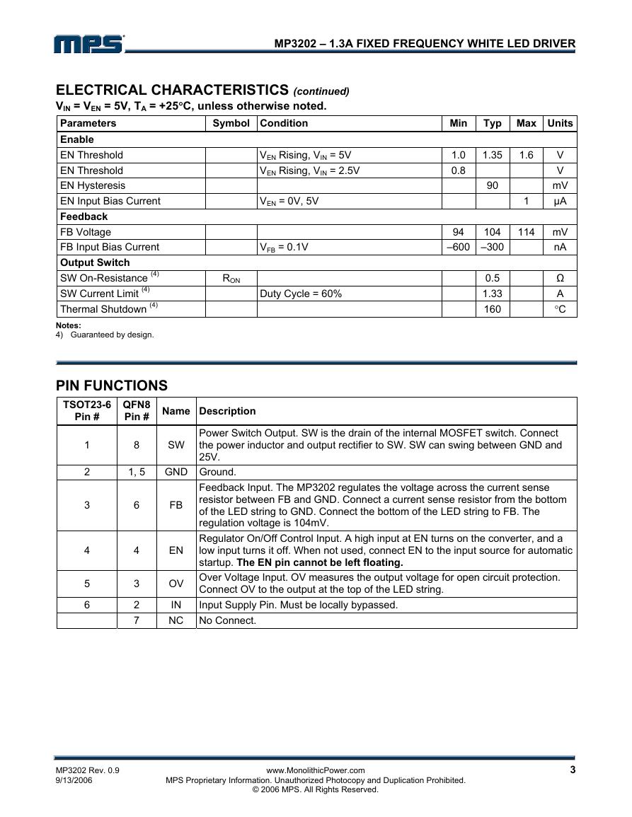
PIN FUNCTIONS
TSOT23-6
Pin #
QFN8
Pin # Name Description
1
2
3
4
5
6
8
SW
Power Switch Output. SW is the drain of the internal MOSFET switch. Connect
the power inductor and output rectifier to SW. SW can swing between GND and
25V.
1, 5
GND Ground.
FB
EN
Feedback Input. The MP3202 regulates the voltage across the current sense
resistor between FB and GND. Connect a current sense resistor from the bottom
of the LED string to GND. Connect the bottom of the LED string to FB. The
regulation voltage is 104mV.
Regulator On/Off Control Input. A high input at EN turns on the converter, and a
low input turns it off. When not used, connect EN to the input source for automatic
startup. The EN pin cannot be left floating.
OV Over Voltage Input. OV measures the output voltage for open circuit protection.
IN
NC No Connect.
Connect OV to the output at the top of the LED string.
Input Supply Pin. Must be locally bypassed.
6
4
3
2
7
MP3202 Rev. 0.9
9/13/2006
MPS Proprietary Information. Unauthorized Photocopy and Duplication Prohibited.
www.MonolithicPower.com
© 2006 MPS. All Rights Reserved.
3
�
MP3202 – 1.3A FIXED FREQUENCY WHITE LED DRIVER
OPERATION
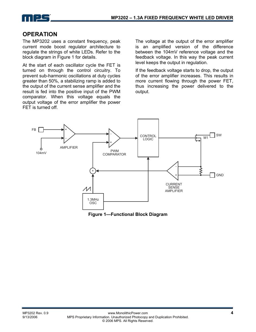
The MP3202 uses a constant frequency, peak
current mode boost regulator architecture to
regulate the strings of white LEDs. Refer to the
block diagram in Figure 1 for details.
At the start of each oscillator cycle the FET is
turned on through the control circuitry. To
prevent sub-harmonic oscillations at duty cycles
greater than 50%, a stabilizing ramp is added to
the output of the current sense amplifier and the
result is fed into the positive input of the PWM
comparator. When
the
output voltage of the error amplifier the power
FET is turned off.
this voltage equals
FB
+
-
AMPLIFIER
104mV
-
+
PWM
COMPARATOR
The voltage at the output of the error amplifier
is an amplified version of
the difference
between the 104mV reference voltage and the
feedback voltage. In this way the peak current
level keeps the output in regulation.
If the feedback voltage starts to drop, the output
of the error amplifier increases. This results in
more current flowing through the power FET,
thus increasing the power delivered to the
output.
CONTROL
LOGIC
SW
M1
+
1.3MHz
OSC
-
+
CURRENT
SENSE
AMPLIFIER
Figure 1—Functional Block Diagram
MP3202 Rev. 0.9
9/13/2006
MPS Proprietary Information. Unauthorized Photocopy and Duplication Prohibited.
www.MonolithicPower.com
© 2006 MPS. All Rights Reserved.
GND
4
�
MP3202 – 1.3A FIXED FREQUENCY WHITE LED DRIVER
APPLICATION INFORMATION
VIN
4V to 6V
OFF ON
MBR0520
9 Strings
Total
IN
EN
GND
MP3202
SW
OV
FB
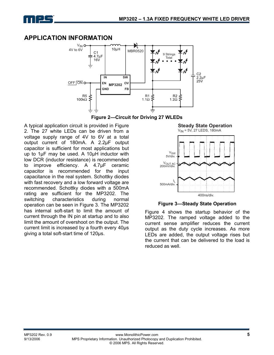
Figure 2—Circuit for Driving 27 WLEDs
is
recommended
for
A typical application circuit is provided in Figure
2. The 27 white LEDs can be driven from a
voltage supply range of 4V to 6V at a total
output current of 180mA. A 2.2µF output
capacitor is sufficient for most applications but
up to 1µF may be used. A 10µH inductor with
low DCR (inductor resistance) is recommended
to
improve efficiency. A 4.7µF ceramic
capacitor
input
capacitance in the real system. Schottky diodes
with fast recovery and a low forward voltage are
recommended. Schottky diodes with a 500mA
rating are sufficient
the MP3202. The
switching
normal
operation can be seen in Figure 3. The MP3202
has internal soft-start to limit the amount of
current through the IN pin at startup and to also
limit the amount of overshoot on the output. The
current limit is increased by a fourth every 40µs
giving a total soft-start time of 120µs.
for
characteristics
during
the
Steady State Operation
VIN = 5V, 27 LEDS, 180mA
VSW
5V/div.
VOUT AC
200mV/div.
IL
500mA/div.
Figure 3—Steady State Operation
400ns/div.
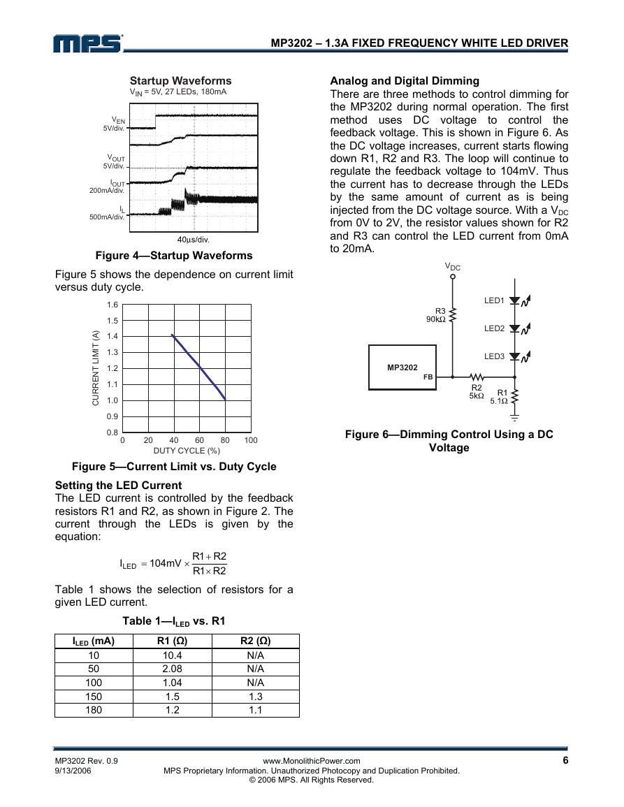
Figure 4 shows the startup behavior of the
MP3202. The ramped voltage added to the
current sense amplifier reduces the current
output as the duty cycle increases. As more
LEDs are added, the output voltage rises but
the current that can be delivered to the load is
reduced as well.
MP3202 Rev. 0.9
9/13/2006
MPS Proprietary Information. Unauthorized Photocopy and Duplication Prohibited.
www.MonolithicPower.com
© 2006 MPS. All Rights Reserved.
5
�
MP3202 – 1.3A FIXED FREQUENCY WHITE LED DRIVER
Startup Waveforms
VIN = 5V, 27 LEDs, 180mA
VEN
5V/div.
VOUT
5V/div.
IOUT
200mA/div.
IL
500mA/div.
Figure 4—Startup Waveforms
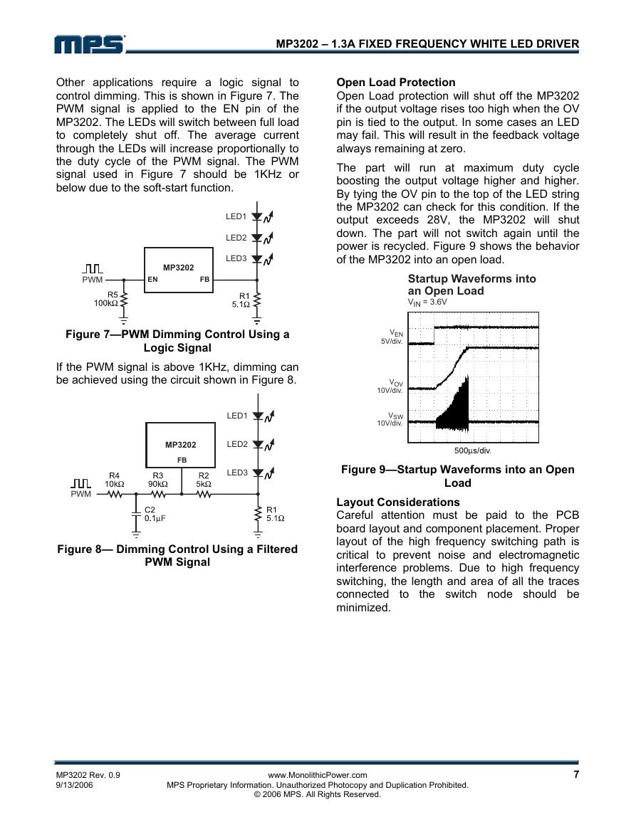
Figure 5 shows the dependence on current limit
versus duty cycle.
)
A
I
I
(
T
M
L
T
N
E
R
R
U
C
1.6
1.5
1.4
1.3
1.2
1.1
1.0
0.9
0.8
0
20
40
60
DUTY CYCLE (%)
80
100
Figure 5—Current Limit vs. Duty Cycle
to control
Analog and Digital Dimming
There are three methods to control dimming for
the MP3202 during normal operation. The first
method uses DC voltage
the
feedback voltage. This is shown in Figure 6. As
the DC voltage increases, current starts flowing
down R1, R2 and R3. The loop will continue to
regulate the feedback voltage to 104mV. Thus
the current has to decrease through the LEDs
by the same amount of current as is being
injected from the DC voltage source. With a VDC
from 0V to 2V, the resistor values shown for R2
and R3 can control the LED current from 0mA
to 20mA.
VDC
LED1
LED2
LED3
MP3202
FB
Figure 6—Dimming Control Using a DC
Voltage
Setting the LED Current
The LED current is controlled by the feedback
resistors R1 and R2, as shown in Figure 2. The
current through the LEDs is given by the
equation:
ILED
=
104
mV
×
2R1R
2R1R
+
×
Table 1 shows the selection of resistors for a
given LED current.
Table 1—ILED vs. R1
ILED (mA)
10
50
100
150
180
MP3202 Rev. 0.9
9/13/2006
R1 (Ω)
10.4
2.08
1.04
1.5
1.2
R2 (Ω)
N/A
N/A
N/A
1.3
1.1
MPS Proprietary Information. Unauthorized Photocopy and Duplication Prohibited.
www.MonolithicPower.com
© 2006 MPS. All Rights Reserved.
6
�
MP3202 – 1.3A FIXED FREQUENCY WHITE LED DRIVER
Other applications require a logic signal to
control dimming. This is shown in Figure 7. The
PWM signal is applied to the EN pin of the
MP3202. The LEDs will switch between full load
to completely shut off. The average current
through the LEDs will increase proportionally to
the duty cycle of the PWM signal. The PWM
signal used in Figure 7 should be 1KHz or
below due to the soft-start function.
LED1
LED2
LED3
PWM
MP3202
EN
FB
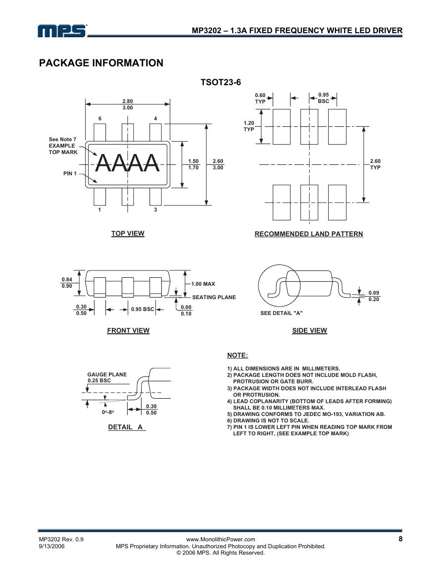
Open Load Protection
Open Load protection will shut off the MP3202
if the output voltage rises too high when the OV
pin is tied to the output. In some cases an LED
may fail. This will result in the feedback voltage
always remaining at zero.
The part will run at maximum duty cycle
boosting the output voltage higher and higher.
By tying the OV pin to the top of the LED string
the MP3202 can check for this condition. If the
output exceeds 28V, the MP3202 will shut
down. The part will not switch again until the
power is recycled. Figure 9 shows the behavior
of the MP3202 into an open load.
Startup Waveforms into
an Open Load
VIN = 3.6V
Figure 7—PWM Dimming Control Using a
Logic Signal
If the PWM signal is above 1KHz, dimming can
be achieved using the circuit shown in Figure 8.
MP3202
FB
LED1
LED2
LED3
PWM
Figure 8— Dimming Control Using a Filtered
PWM Signal
VEN
5V/div.
VOV
10V/div.
VSW
10V/div.
Figure 9—Startup Waveforms into an Open
Load
Layout Considerations
Careful attention must be paid to the PCB
board layout and component placement. Proper
layout of the high frequency switching path is
critical to prevent noise and electromagnetic
interference problems. Due to high frequency
switching, the length and area of all the traces
connected
the switch node should be
minimized.
to
MP3202 Rev. 0.9
9/13/2006
MPS Proprietary Information. Unauthorized Photocopy and Duplication Prohibited.
www.MonolithicPower.com
© 2006 MPS. All Rights Reserved.
7
�
MP3202 – 1.3A FIXED FREQUENCY WHITE LED DRIVER
PACKAGE INFORMATION
2.80
3.00
6
4
TSOT23-6
0.60
TYP
1.20
TYP
0.95
BSC
See Note 7
EXAMPLE
TOP MARK
PIN 1
AAAA
1.50
1.70
2.60
3.00
1
3
TOP VIEW
RECOMMENDED LAND PATTERN
0.84
0.90
1.00 MAX
SEATING PLANE
0.30
0.50
0.95 BSC
0.00
0.10
FRONT VIEW
SEE DETAIL "A"
SIDE VIEW
2.60
TYP
0.09
0.20
GAUGE PLANE
0.25 BSC
0o-8o
0.30
0.50
DETAIL A
NOTE:
1) ALL DIMENSIONS ARE IN MILLIMETERS.
2) PACKAGE LENGTH DOES NOT INCLUDE MOLD FLASH,
PROTRUSION OR GATE BURR.
3) PACKAGE WIDTH DOES NOT INCLUDE INTERLEAD FLASH
OR PROTRUSION.
4) LEAD COPLANARITY (BOTTOM OF LEADS AFTER FORMING)
SHALL BE 0.10 MILLIMETERS MAX.
5) DRAWING CONFORMS TO JEDEC MO-193, VARIATION AB.
6) DRAWING IS NOT TO SCALE.
7) PIN 1 IS LOWER LEFT PIN WHEN READING TOP MARK FROM
LEFT TO RIGHT, (SEE EXAMPLE TOP MARK)
MP3202 Rev. 0.9
9/13/2006
MPS Proprietary Information. Unauthorized Photocopy and Duplication Prohibited.
www.MonolithicPower.com
© 2006 MPS. All Rights Reserved.
8
�



 V2版本原理图(Capacitive-Fingerprint-Reader-Schematic_V2).pdf
 摄像头工作原理.doc
 VL53L0X简要说明(En.FLVL53L00216).pdf
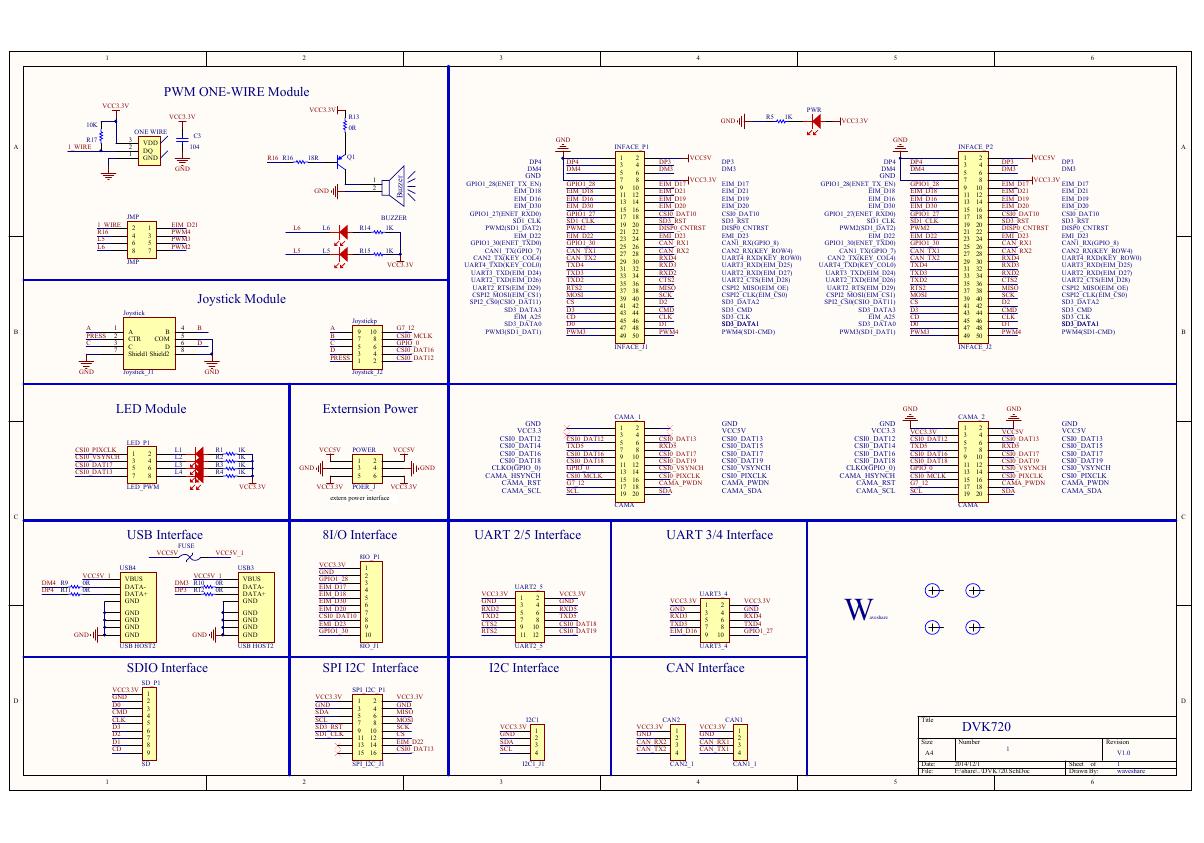 原理图(DVK720-Schematic).pdf
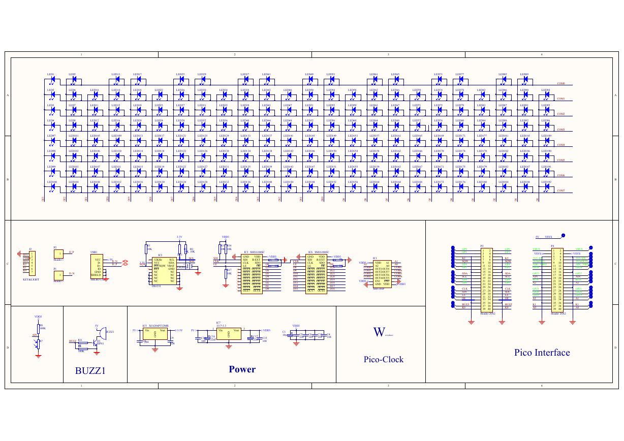 原理图(Pico-Clock-Green-Schdoc).pdf
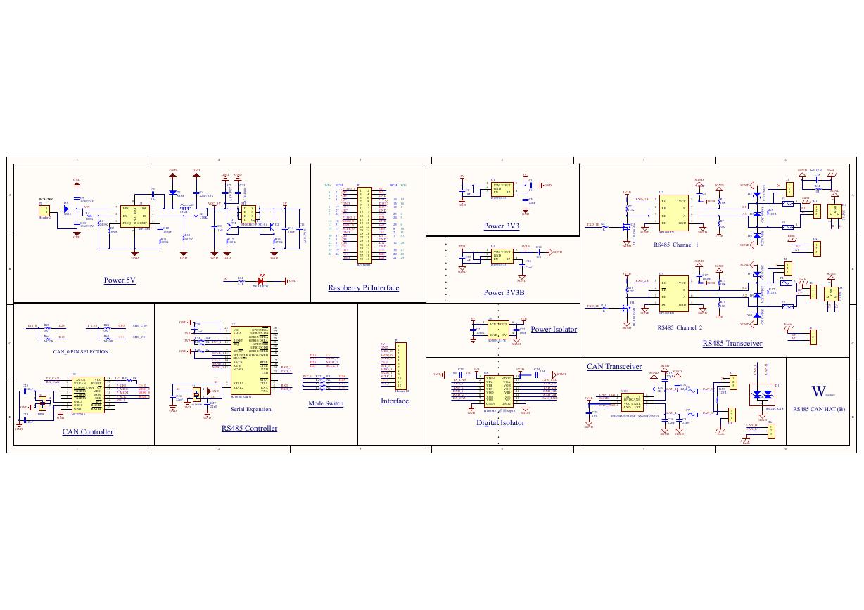 原理图(RS485-CAN-HAT-B-schematic).pdf
 File:SIM7500_SIM7600_SIM7800 Series_SSL_Application Note_V2.00.pdf
 ADS1263(Ads1262).pdf
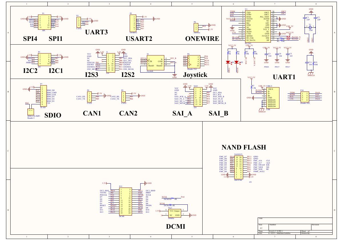 原理图(Open429Z-D-Schematic).pdf
 用户手册(Capacitive_Fingerprint_Reader_User_Manual_CN).pdf
 CY7C68013A(英文版)(CY7C68013A).pdf
 TechnicalReference_Dem.pdf