Product Specifications
Customer
Description
Model Name
Date
Revision
Standard
7.5” E-PAPER DISPLAY
7.5inch HD e-Paper (B)
2019/03/30
1.1
10F, International Science & Technology Building, Fuhong Rd, Futian District,
Shenzhen, China
Email: sales@waveshare.com
Website: www.waveshare.com
7.5inch HD e-Paper (B)1/36�
Table of Contents
1. General Description....................................................
1.1 Overview............................................................
1.2 Feature ..............................................................
1.3 Mechanical Specification........................................
1.4 Mechanical Drawing of EPD module .......................
1.5 Input/Output Terminals........................................
1.6 Reference Circuit ................................................
2. Environmental............................................................
2.1 Handling, Safety and Environmental Requirements...
2.2 Reliability test.....................................................
3. Electrical Characteristics .............................................
3.1 Absolute maximum rating.....................................
3.2 DC Characteristics..............................................
3.3 Serial Peripheral Interface Timing .........................
3.4 Power Consumption..............................................
4
4
4
4
5
6
8
9
9
11
12
12
12
13
13
3.5 MCU Interface..................................................... 14
18
18
19
31
31
32
32
33
35
36
4. Typical Operating Sequence.........................................
4.1 Normal Operation Flow.........................................
5. Command Table.........................................................
6. Optical characteristics.................................................
6.1 Specifications ....................................................
6.2 Definition of contrast ratio...................................
6.3 Reflection Ratio..................................................
7. Point and line standard...............................................
8. Packing.....................................................................
9. Precautions ..............................................................
7.5inch HD e-Paper (B)2/36�
Version
Content
Date
Producer
1.0
1.1
New release
2019/10/14
Updating: 1.6 Reference Circuit 2020/03/30
7.5inch HD e-Paper (B)3/36�
1. General Description
1.1 Overview
This is an Active Matrix Electrophoretic Display (AMEPD), with interface and a
reference system design. The 7.5” active area contains528×880 pixels, and has 1-
bit B/W/R full display capabilities. An integrated circuit contains gate buffer, source
buffer, interface, timing control logic, oscillator, DC-DC. SRAM.LUT, VCOM and
border are supplied with each panel.
1.2 Features
● 528×880 pixels display
● High contrast
● High reflectance
● Ultra wide viewing angle
● Ultra low power consumption
● Pure reflective mode
● Bi-stable display
● Commercial temperature range
● Landscape, portrait modes
● Hard-coat antiglare display surface
● Ultra Low current deep sleep mode
● On chip display RAM
● Low voltage detect for supply voltage
● High voltage ready detect for driving voltage
● Internal temperature sensor
● 10-byte OTP space for module identification
● Waveform stored in On-chip OTP
● Serial peripheral interface available
● On-chip oscillator
● On-chip booster and regulator control for generating VCOM, Gate and Source
driving voltage
● I2C signal master interface to read external temperature sensor/built-in
temperature sensor
1.3 Mechanical Specifications
Parameter
Screen Size
Specifications
7.5
Display Resolution
880(V)×528(H)
Active Area
Pixel Pitch
163.24(H)×97.94(V)
0.1855×0.1855
Pixel Configuration
Outline Dimension 170.2(H)×111.2 (V) ×1.25(D)
Rectangle
Weight
31±0.2
Unit
Inch
Pixel
mm
mm
mm
g
Remark
Dpi:137
7.5inch HD e-Paper (B)4/36�
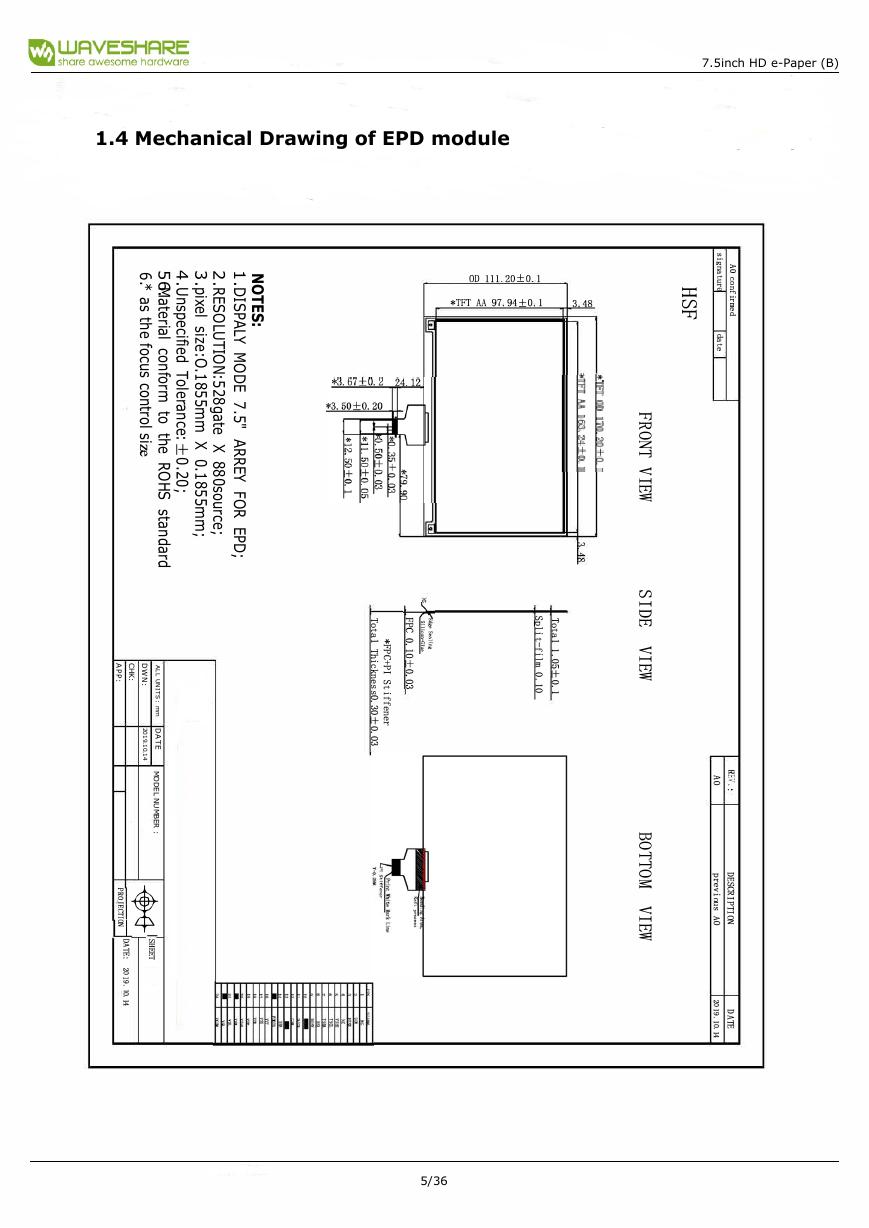
1.4 Mechanical Drawing of EPD module
N
O
T
E
S
:
3
.
p
x
e
l
i
s
i
z
e
:
O
.
1
8
5
5
m
m
X
0
.
1
8
5
5
m
m
;
2
.
R
E
S
O
L
U
T
I
O
N
:
5
2
8
g
a
t
e
X
8
8
0
s
o
u
r
c
e
;
1
.
D
I
S
P
A
L
Y
M
O
D
E
7
.
5
"
A
R
R
E
Y
F
O
R
E
P
D
;
6
.
*
a
s
t
h
e
f
o
c
u
s
c
o
n
t
r
o
l
s
i
在
5
6
.M
a
t
e
r
i
a
l
c
o
n
f
o
r
m
t
o
4
.
U
n
s
p
e
c
i
f
i
e
d
T
o
e
r
a
n
c
e
:
l
t
h
士
e
0
R
.
O
2
H
0
;
S
s
t
a
n
d
a
r
d
A
P
P
:
C
H
K
:
D
W
N
:
2
0
1
9
.
1
0
.
1
4
A
L
L
U
N
I
T
S
:
m
m
D
A
T
E
M
O
D
E
L
N
U
M
B
E
R
:
妇
了
可
勹
IS
H
E
E
T
D
A
T
E
2
:
0
1
9
.
1
0
.
1
4
l·o廿oz"]]]云0
1·o廿v6"l6 VV lill *
8v "E
*一
s
1
g
n
a
t
u
r
d
a
t
e
A
O
c
o
n
f
i
r
m
e
d
H
S
F
S
T
p
o
l
t
i
a
1
t
l
.
0
-
f
5
+
0
i
0
.
1
l
.
1
0
m
T
o
t
a
T
l
h
i
c
k
n
e
3
s
0
+
s
0
O
.
0
.
3
*
F
P
C
+
S
P
t
I
i
f
f
e
n
e
r
F
R
O
N
V
T
I
E
W
S
I
D
E
V
I
E
W
B
O
T
T
O
V
M
I
E
W
A
O
R
二
V
.
p
r
e
v
i
A
o
O
u
s
D
E
S
CR
I
P
T
I
ON
D
A
T
E
2
0
1
9
.
1
0
.
1
4
7.5inch HD e-Paper (B)5/36�
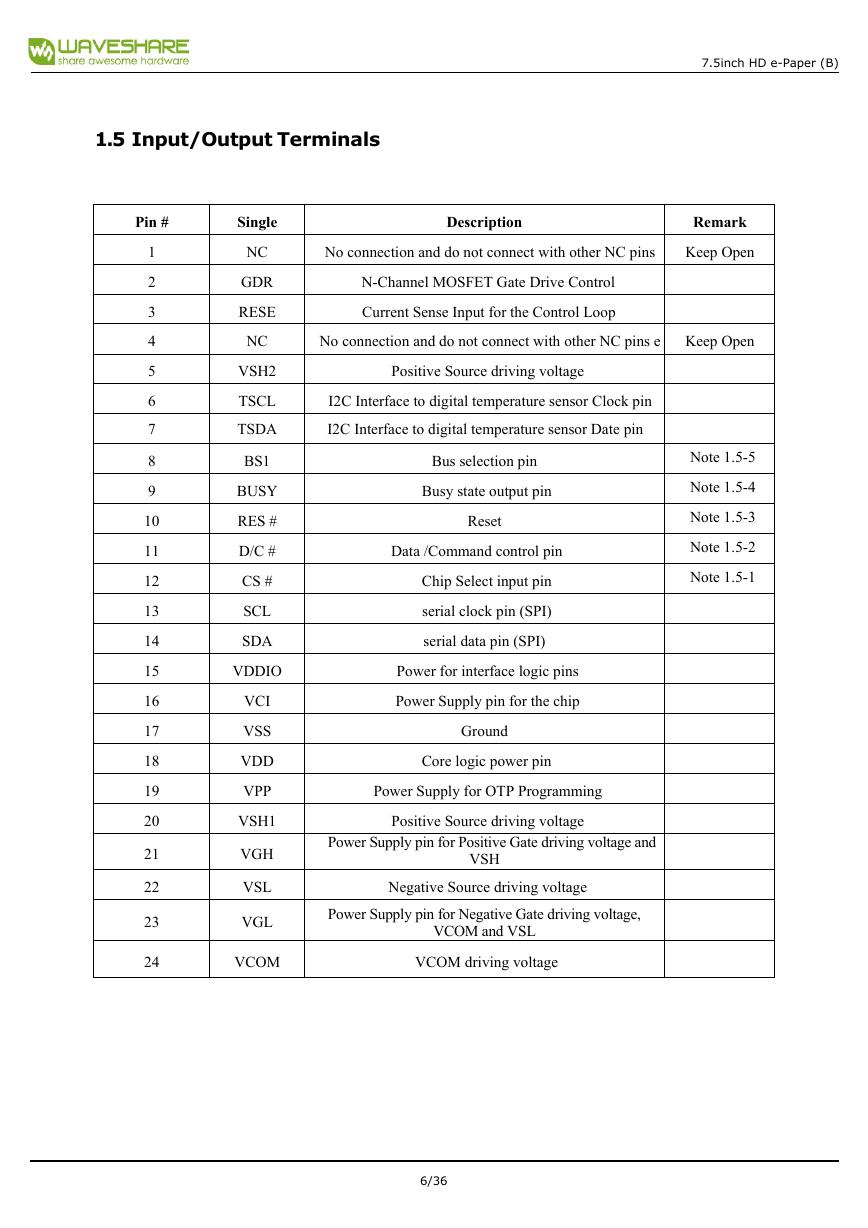
1.5 Input/Output Terminals
Pin #
1
2
3
4
5
6
7
8
9
10
11
12
13
14
15
16
17
18
19
20
21
22
23
24
Single
NC
GDR
RESE
NC
VSH2
TSCL
TSDA
BS1
BUSY
RES #
D/C #
CS #
SCL
SDA
VDDIO
VCI
VSS
VDD
VPP
VSH1
VGH
VSL
VGL
Description
No connection and do not connect with other NC pins
N-Channel MOSFET Gate Drive Control
Current Sense Input for the Control Loop
Remark
Keep Open
No connection and do not connect with other NC pins e Keep Open
Positive Source driving voltage
I2C Interface to digital temperature sensor Clock pin
I2C Interface to digital temperature sensor Date pin
Note 1.5-5
Note 1.5-4
Note 1.5-3
Note 1.5-2
Note 1.5-1
Bus selection pin
Busy state output pin
Reset
Data /Command control pin
Chip Select input pin
serial clock pin (SPI)
serial data pin (SPI)
Power for interface logic pins
Power Supply pin for the chip
Ground
Core logic power pin
Power Supply for OTP Programming
Positive Source driving voltage
Power Supply pin for Positive Gate driving voltage and
VSH
Negative Source driving voltage
Power Supply pin for Negative Gate driving voltage,
VCOM and VSL
VCOM
VCOM driving voltage
7.5inch HD e-Paper (B)6/36�
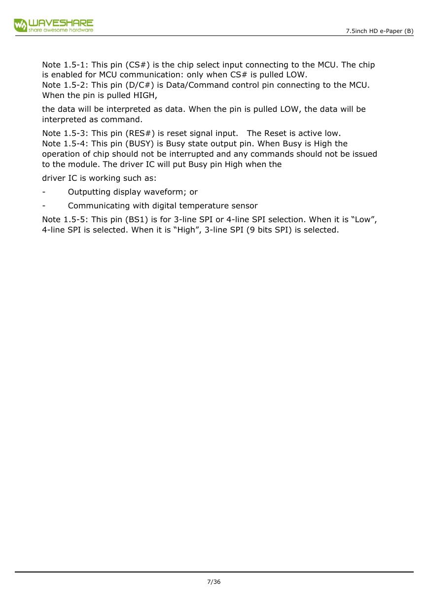
Note 1.5-1: This pin (CS#) is the chip select input connecting to the MCU. The chip
is enabled for MCU communication: only when CS# is pulled LOW.
Note 1.5-2: This pin (D/C#) is Data/Command control pin connecting to the MCU.
When the pin is pulled HIGH,
the data will be interpreted as data. When the pin is pulled LOW, the data will be
interpreted as command.
Note 1.5-3: This pin (RES#) is reset signal input. The Reset is active low.
Note 1.5-4: This pin (BUSY) is Busy state output pin. When Busy is High the
operation of chip should not be interrupted and any commands should not be issued
to the module. The driver IC will put Busy pin High when the
driver IC is working such as:
-
-
Note 1.5-5: This pin (BS1) is for 3-line SPI or 4-line SPI selection. When it is “Low”,
4-line SPI is selected. When it is “High”, 3-line SPI (9 bits SPI) is selected.
Outputting display waveform; or
Communicating with digital temperature sensor
7.5inch HD e-Paper (B)7/36�
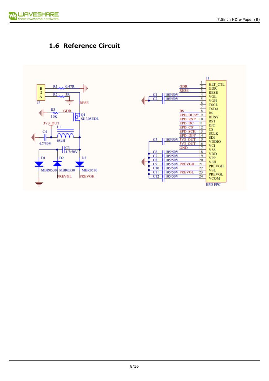
1.6 Reference Circuit
7.5inch HD e-Paper (B)8/36�



 V2版本原理图(Capacitive-Fingerprint-Reader-Schematic_V2).pdf
 摄像头工作原理.doc
 VL53L0X简要说明(En.FLVL53L00216).pdf
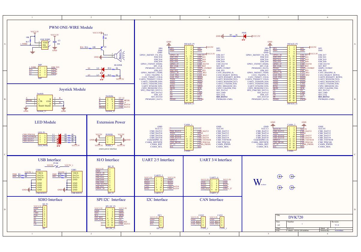 原理图(DVK720-Schematic).pdf
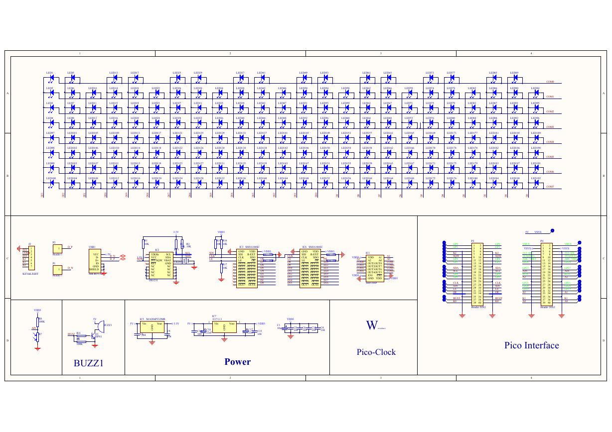 原理图(Pico-Clock-Green-Schdoc).pdf
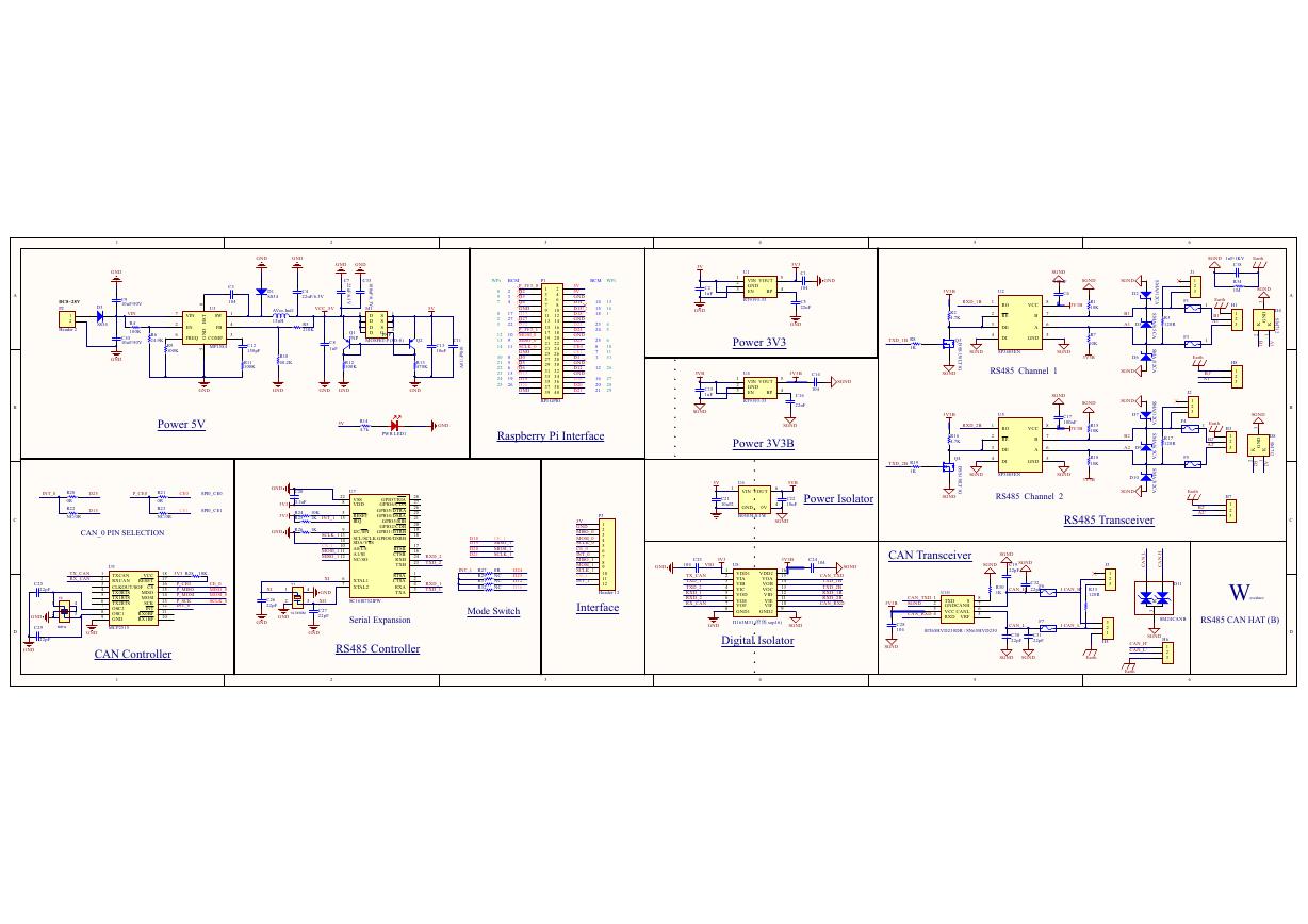 原理图(RS485-CAN-HAT-B-schematic).pdf
 File:SIM7500_SIM7600_SIM7800 Series_SSL_Application Note_V2.00.pdf
 ADS1263(Ads1262).pdf
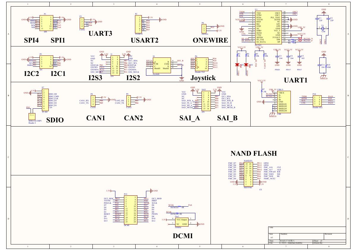 原理图(Open429Z-D-Schematic).pdf
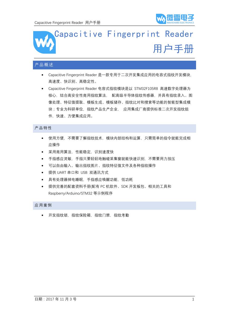 用户手册(Capacitive_Fingerprint_Reader_User_Manual_CN).pdf
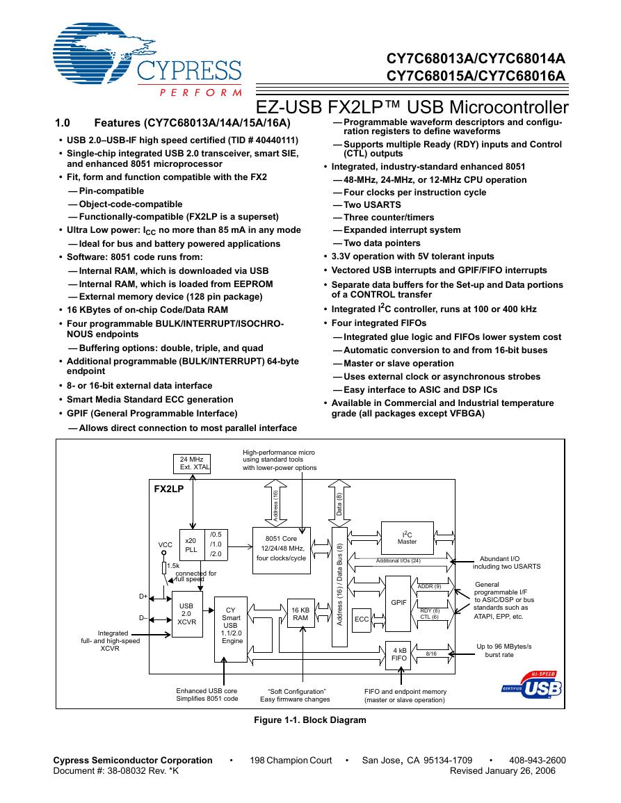 CY7C68013A(英文版)(CY7C68013A).pdf
 TechnicalReference_Dem.pdf