Features
• Single 2.5V - 3.6V or 2.7V - 3.6V Supply
RapidS™ Serial Interface: 66 MHz Maximum Clock Frequency
– SPI Compatible Modes 0 and 3
User Configurable Page Size
– 512 Bytes per Page
– 528 Bytes per Page
– Page Size Can Be Factory Pre-configured for 512 Bytes
Page Program Operation
– Intelligent Programming Operation
– 4,096 Pages (512/528 Bytes/Page) Main Memory
Flexible Erase Options
– Page Erase (512 Bytes)
– Block Erase (4 Kbytes)
– Sector Erase (128 Kbytes)
– Chip Erase (16 Mbits)
Two SRAM Data Buffers (512/528 Bytes)
– Allows Receiving of Data while Reprogramming the Flash Array
Continuous Read Capability through Entire Array
– Ideal for Code Shadowing Applications
Low-power Dissipation
– 7 mA Active Read Current Typical
– 25 µA Standby Current Typical
– 9 µA Deep Power Down Typical
Hardware and Software Data Protection Features
– Individual Sector
Sector Lockdown for Secure Code and Data Storage
– Individual Sector
Security: 128-byte Security Register
– 64-byte User Programmable Space
– Unique 64-byte Device Identifier
JEDEC Standard Manufacturer and Device ID Read
100,000 Program/Erase Cycles Per Page Minimum
Data Retention – 20 Years
Industrial Temperature Range
Green (Pb/Halide-free/RoHS Compliant) Packaging Options
16-megabit
2.5-volt or
2.7-volt
DataFlash®
AT45DB161D
1. Description
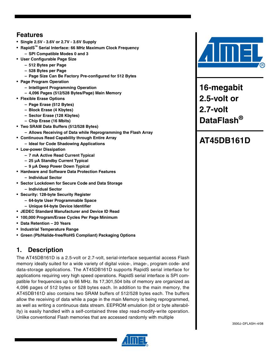
The AT45DB161D is a 2.5-volt or 2.7-volt, serial-interface sequential access Flash
memory ideally suited for a wide variety of digital voice-, image-, program code- and
data-storage applications. The AT45DB161D supports RapidS serial interface for
applications requiring very high speed operations. RapidS serial interface is SPI com-
patible for frequencies up to 66 MHz. Its 17,301,504 bits of memory are organized as
4,096 pages of 512 bytes or 528 bytes each. In addition to the main memory, the
AT45DB161D also contains two SRAM buffers of 512/528 bytes each. The buffers
allow the receiving of data while a page in the main Memory is being reprogrammed,
as well as writing a continuous data stream. EEPROM emulation (bit or byte alterabil-
ity) is easily handled with a self-contained three step read-modify-write operation.
Unlike conventional Flash memories that are accessed randomly with multiple
3500J–DFLASH–4/08
�
address lines and a parallel interface, the DataFlash uses a RapidS serial interface to sequen-
tially access its data. The simple sequential access dramatically reduces active pin count,
facilitates hardware layout, increases system reliability, minimizes switching noise, and reduces
package size. The device is optimized for use in many commercial and industrial applications
where high-density, low-pin count, low-voltage and low-power are essential.
To allow for simple in-system reprogrammability, the AT45DB161D does not require high input
voltages for programming. The device operates from a single power supply, 2.5V to 3.6V or 2.7V
to 3.6V, for both the program and read operations. The AT45DB161D is enabled through the
chip select pin (CS) and accessed via a three-wire interface consisting of the Serial Input (SI),
Serial Output (SO), and the Serial Clock (SCK).
All programming and erase cycles are self-timed.
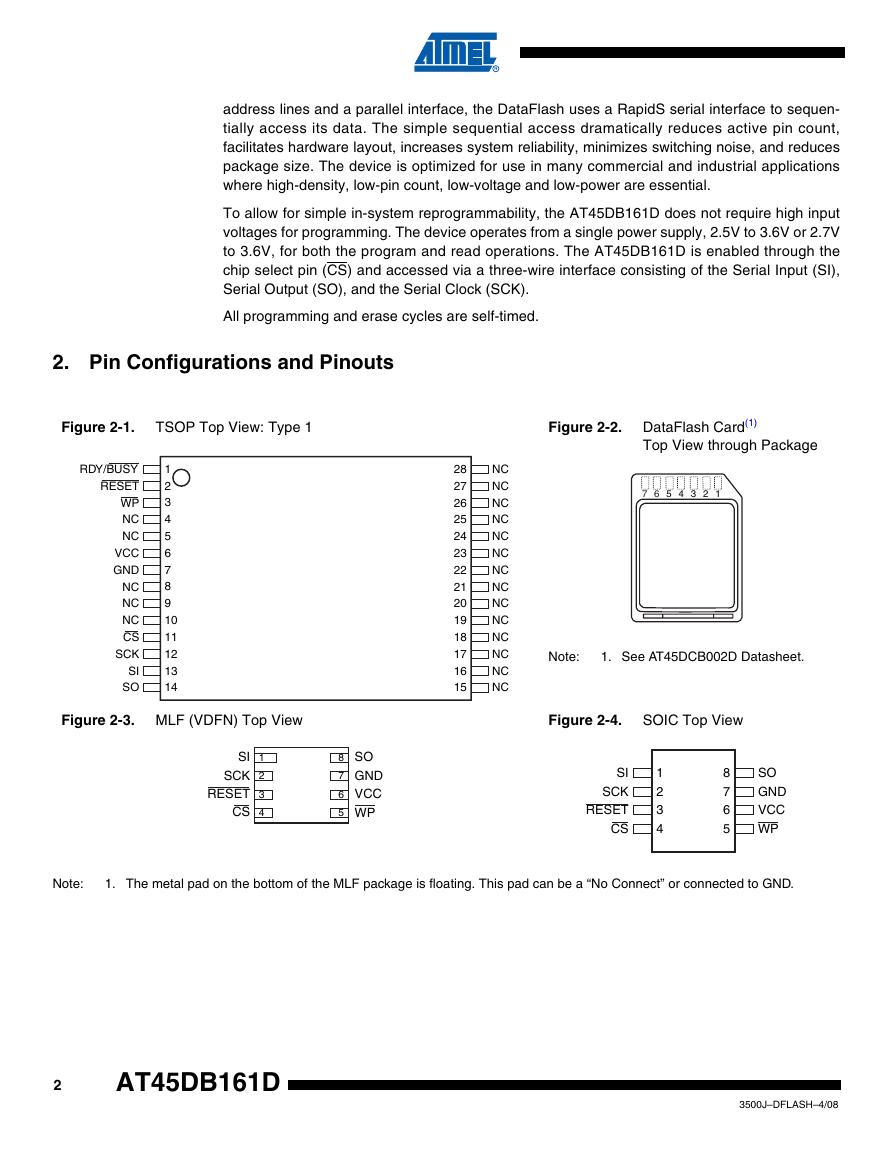
2. Pin Configurations and Pinouts
Figure 2-1.
TSOP Top View: Type 1
RDY/BUSY
RESET
WP
NC
NC
VCC
GND
NC
NC
NC
CS
SCK
SI
SO
1
2
3
4
5
6
7
8
9
10
11
12
13
14
Figure 2-2. DataFlash Card(1)
Top View through Package
7 6 5 4 3 2 1
Note:
1. See AT45DCB002D Datasheet.
28
27
26
25
24
23
22
21
20
19
18
17
16
15
NC
NC
NC
NC
NC
NC
NC
NC
NC
NC
NC
NC
NC
NC
Figure 2-3. MLF (VDFN) Top View
Figure 2-4.
SOIC Top View
SI
SCK
RESET
CS
1
2
3
4
8
7
6
5
SO
GND
VCC
WP
SI
SCK
RESET
CS
1
2
3
4
8
7
6
5
SO
GND
VCC
WP
Note:
1. The metal pad on the bottom of the MLF package is floating. This pad can be a “No Connect” or connected to GND.
2
AT45DB161D
3500J–DFLASH–4/08
�
AT45DB161D
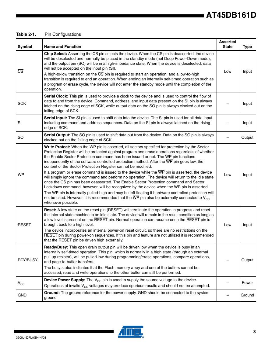
Table 2-1.
Pin Configurations
Symbol
CS
SCK
SI
SO
WP
RESET
RDY/BUSY
VCC
GND
Name and Function
Chip Select: Asserting the CS pin selects the device. When the CS pin is deasserted, the device
will be deselected and normally be placed in the standby mode (not Deep Power-Down mode),
and the output pin (SO) will be in a high-impedance state. When the device is deselected, data
will not be accepted on the input pin (SI).
A high-to-low transition on the CS pin is required to start an operation, and a low-to-high
transition is required to end an operation. When ending an internally self-timed operation such as
a program or erase cycle, the device will not enter the standby mode until the completion of the
operation.
Serial Clock: This pin is used to provide a clock to the device and is used to control the flow of
data to and from the device. Command, address, and input data present on the SI pin is always
latched on the rising edge of SCK, while output data on the SO pin is always clocked out on the
falling edge of SCK.
Serial Input: The SI pin is used to shift data into the device. The SI pin is used for all data input
including command and address sequences. Data on the SI pin is always latched on the rising
edge of SCK.
Serial Output: The SO pin is used to shift data out from the device. Data on the SO pin is always
clocked out on the falling edge of SCK.
Write Protect: When the WP pin is asserted, all sectors specified for protection by the Sector
Protection Register will be protected against program and erase operations regardless of whether
the Enable Sector Protection command has been issued or not. The WP pin functions
independently of the software controlled protection method. After the WP pin goes low, the
content of the Sector Protection Register cannot be modified.
If a program or erase command is issued to the device while the WP pin is asserted, the device
will simply ignore the command and perform no operation. The device will return to the idle state
once the CS pin has been deasserted. The Enable Sector Protection command and Sector
Lockdown command, however, will be recognized by the device when the WP pin is asserted.
The WP pin is internally pulled-high and may be left floating if hardware controlled protection will
not be used. However, it is recommended that the WP pin also be externally connected to VCC
whenever possible.
Reset: A low state on the reset pin (RESET) will terminate the operation in progress and reset
the internal state machine to an idle state. The device will remain in the reset condition as long as
a low level is present on the RESET pin. Normal operation can resume once the RESET pin is
brought back to a high level.
The device incorporates an internal power-on reset circuit, so there are no restrictions on the
RESET pin during power-on sequences. If this pin and feature are not utilized it is recommended
that the RESET pin be driven high externally.
Ready/Busy: This open drain output pin will be driven low when the device is busy in an
internally self-timed operation. This pin, which is normally in a high state (through an external
pull-up resistor), will be pulled low during programming/erase operations, compare operations,
and page-to-buffer transfers.
The busy status indicates that the Flash memory array and one of the buffers cannot be
accessed; read and write operations to the other buffer can still be performed.
Device Power Supply: The VCC pin is used to supply the source voltage to the device.
Operations at invalid VCC voltages may produce spurious results and should not be attempted.
Ground: The ground reference for the power supply. GND should be connected to the system
ground.
3500J–DFLASH–4/08
Asserted
State
Type
Low
Input
–
–
–
Input
Input
Output
Low
Input
Low
Input
–
–
–
Output
Power
Ground
3
�
3. Block Diagram
WP
FLASH MEMORY ARRAY
PAGE (512/528 BYTES)
BUFFER 1 (512/528 BYTES)
BUFFER 2 (512/528 BYTES)
SCK
CS
RESET
VCC
GND
RDY/BUSY
I/O INTERFACE
SI
SO
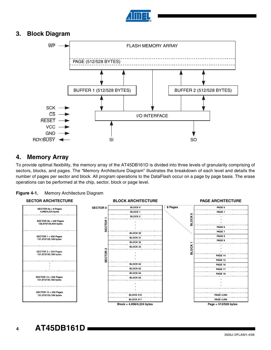
4. Memory Array
To provide optimal flexibility, the memory array of the AT45DB161D is divided into three levels of granularity comprising of
sectors, blocks, and pages. The “Memory Architecture Diagram” illustrates the breakdown of each level and details the
number of pages per sector and block. All program operations to the DataFlash occur on a page by page basis. The erase
operations can be performed at the chip, sector, block or page level.
Figure 4-1. Memory Architecture Diagram
SECTOR ARCHITECTURE
BLOCK ARCHITECTURE
PAGE ARCHITECTURE
SECTOR 0a = 8 Pages
4,096/4,224 bytes
SECTOR 0b = 248 Pages
126,976/130,944 bytes
SECTOR 1 = 256 Pages
131,072/135,168 bytes
SECTOR 2 = 256 Pages
131,072/135,168 bytes
SECTOR 14 = 256 Pages
131,072/135,168 bytes
SECTOR 15 = 256 Pages
131,072/135,168 bytes
SECTOR 0
1
R
O
T
C
E
S
2
R
O
T
C
E
S
BLOCK 0
BLOCK 1
BLOCK 2
BLOCK 30
BLOCK 31
BLOCK 32
BLOCK 33
BLOCK 62
BLOCK 63
BLOCK 64
BLOCK 65
8 Pages
0
K
C
O
L
B
1
K
C
O
L
B
PAGE 0
PAGE 1
PAGE 6
PAGE 7
PAGE 8
PAGE 9
PAGE 14
PAGE 15
PAGE 16
PAGE 17
PAGE 18
BLOCK 510
BLOCK 511
Block = 4,096/4,224 bytes
PAGE 4,094
PAGE 4,095
Page = 512/528 bytes
4
AT45DB161D
3500J–DFLASH–4/08
�
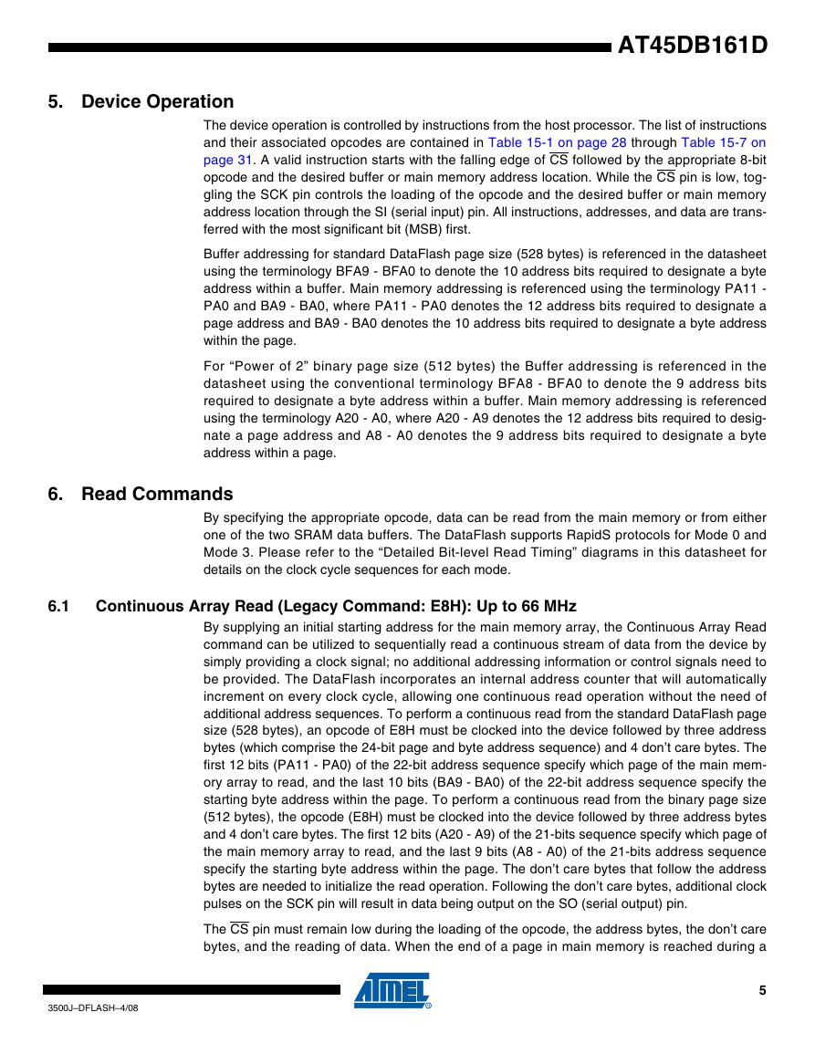
5. Device Operation
AT45DB161D
The device operation is controlled by instructions from the host processor. The list of instructions
and their associated opcodes are contained in Table 15-1 on page 28 through Table 15-7 on
page 31. A valid instruction starts with the falling edge of CS followed by the appropriate 8-bit
opcode and the desired buffer or main memory address location. While the CS pin is low, tog-
gling the SCK pin controls the loading of the opcode and the desired buffer or main memory
address location through the SI (serial input) pin. All instructions, addresses, and data are trans-
ferred with the most significant bit (MSB) first.
Buffer addressing for standard DataFlash page size (528 bytes) is referenced in the datasheet
using the terminology BFA9 - BFA0 to denote the 10 address bits required to designate a byte
address within a buffer. Main memory addressing is referenced using the terminology PA11 -
PA0 and BA9 - BA0, where PA11 - PA0 denotes the 12 address bits required to designate a
page address and BA9 - BA0 denotes the 10 address bits required to designate a byte address
within the page.
For “Power of 2” binary page size (512 bytes) the Buffer addressing is referenced in the
datasheet using the conventional terminology BFA8 - BFA0 to denote the 9 address bits
required to designate a byte address within a buffer. Main memory addressing is referenced
using the terminology A20 - A0, where A20 - A9 denotes the 12 address bits required to desig-
nate a page address and A8 - A0 denotes the 9 address bits required to designate a byte
address within a page.
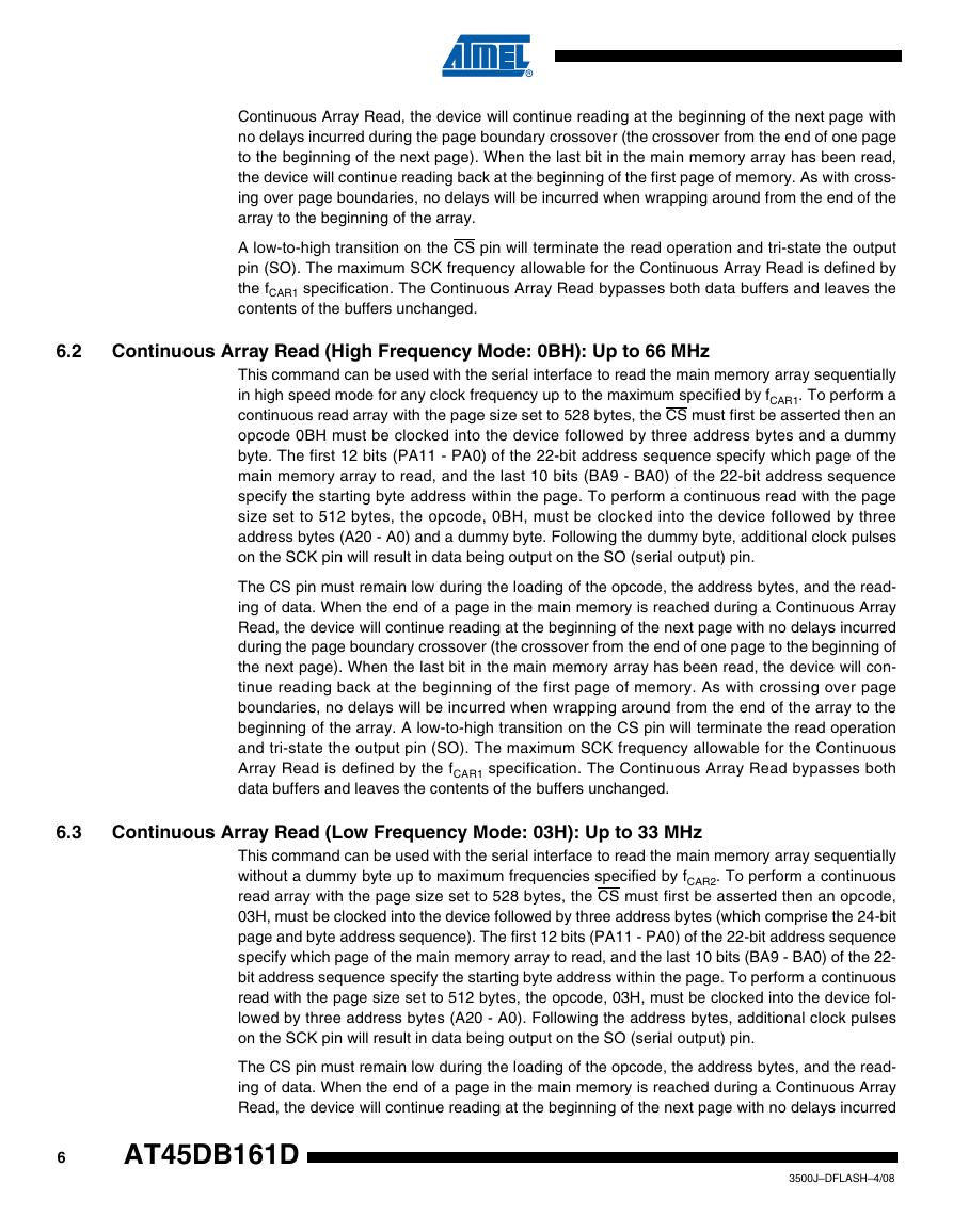
6. Read Commands
By specifying the appropriate opcode, data can be read from the main memory or from either
one of the two SRAM data buffers. The DataFlash supports RapidS protocols for Mode 0 and
Mode 3. Please refer to the “Detailed Bit-level Read Timing” diagrams in this datasheet for
details on the clock cycle sequences for each mode.
6.1
Continuous Array Read (Legacy Command: E8H): Up to 66 MHz
By supplying an initial starting address for the main memory array, the Continuous Array Read
command can be utilized to sequentially read a continuous stream of data from the device by
simply providing a clock signal; no additional addressing information or control signals need to
be provided. The DataFlash incorporates an internal address counter that will automatically
increment on every clock cycle, allowing one continuous read operation without the need of
additional address sequences. To perform a continuous read from the standard DataFlash page
size (528 bytes), an opcode of E8H must be clocked into the device followed by three address
bytes (which comprise the 24-bit page and byte address sequence) and 4 don’t care bytes. The
first 12 bits (PA11 - PA0) of the 22-bit address sequence specify which page of the main mem-
ory array to read, and the last 10 bits (BA9 - BA0) of the 22-bit address sequence specify the
starting byte address within the page. To perform a continuous read from the binary page size
(512 bytes), the opcode (E8H) must be clocked into the device followed by three address bytes
and 4 don’t care bytes. The first 12 bits (A20 - A9) of the 21-bits sequence specify which page of
the main memory array to read, and the last 9 bits (A8 - A0) of the 21-bits address sequence
specify the starting byte address within the page. The don’t care bytes that follow the address
bytes are needed to initialize the read operation. Following the don’t care bytes, additional clock
pulses on the SCK pin will result in data being output on the SO (serial output) pin.
The CS pin must remain low during the loading of the opcode, the address bytes, the don’t care
bytes, and the reading of data. When the end of a page in main memory is reached during a
3500J–DFLASH–4/08
5
�
Continuous Array Read, the device will continue reading at the beginning of the next page with
no delays incurred during the page boundary crossover (the crossover from the end of one page
to the beginning of the next page). When the last bit in the main memory array has been read,
the device will continue reading back at the beginning of the first page of memory. As with cross-
ing over page boundaries, no delays will be incurred when wrapping around from the end of the
array to the beginning of the array.
A low-to-high transition on the CS pin will terminate the read operation and tri-state the output
pin (SO). The maximum SCK frequency allowable for the Continuous Array Read is defined by
the fCAR1 specification. The Continuous Array Read bypasses both data buffers and leaves the
contents of the buffers unchanged.
6.2
Continuous Array Read (High Frequency Mode: 0BH): Up to 66 MHz
This command can be used with the serial interface to read the main memory array sequentially
in high speed mode for any clock frequency up to the maximum specified by fCAR1. To perform a
continuous read array with the page size set to 528 bytes, the CS must first be asserted then an
opcode 0BH must be clocked into the device followed by three address bytes and a dummy
byte. The first 12 bits (PA11 - PA0) of the 22-bit address sequence specify which page of the
main memory array to read, and the last 10 bits (BA9 - BA0) of the 22-bit address sequence
specify the starting byte address within the page. To perform a continuous read with the page
size set to 512 bytes, the opcode, 0BH, must be clocked into the device followed by three
address bytes (A20 - A0) and a dummy byte. Following the dummy byte, additional clock pulses
on the SCK pin will result in data being output on the SO (serial output) pin.
The CS pin must remain low during the loading of the opcode, the address bytes, and the read-
ing of data. When the end of a page in the main memory is reached during a Continuous Array
Read, the device will continue reading at the beginning of the next page with no delays incurred
during the page boundary crossover (the crossover from the end of one page to the beginning of
the next page). When the last bit in the main memory array has been read, the device will con-
tinue reading back at the beginning of the first page of memory. As with crossing over page
boundaries, no delays will be incurred when wrapping around from the end of the array to the
beginning of the array. A low-to-high transition on the CS pin will terminate the read operation
and tri-state the output pin (SO). The maximum SCK frequency allowable for the Continuous
Array Read is defined by the fCAR1 specification. The Continuous Array Read bypasses both
data buffers and leaves the contents of the buffers unchanged.
6.3
Continuous Array Read (Low Frequency Mode: 03H): Up to 33 MHz
This command can be used with the serial interface to read the main memory array sequentially
without a dummy byte up to maximum frequencies specified by fCAR2. To perform a continuous
read array with the page size set to 528 bytes, the CS must first be asserted then an opcode,
03H, must be clocked into the device followed by three address bytes (which comprise the 24-bit
page and byte address sequence). The first 12 bits (PA11 - PA0) of the 22-bit address sequence
specify which page of the main memory array to read, and the last 10 bits (BA9 - BA0) of the 22-
bit address sequence specify the starting byte address within the page. To perform a continuous
read with the page size set to 512 bytes, the opcode, 03H, must be clocked into the device fol-
lowed by three address bytes (A20 - A0). Following the address bytes, additional clock pulses
on the SCK pin will result in data being output on the SO (serial output) pin.
The CS pin must remain low during the loading of the opcode, the address bytes, and the read-
ing of data. When the end of a page in the main memory is reached during a Continuous Array
Read, the device will continue reading at the beginning of the next page with no delays incurred
6
AT45DB161D
3500J–DFLASH–4/08
�
AT45DB161D
during the page boundary crossover (the crossover from the end of one page to the beginning of
the next page). When the last bit in the main memory array has been read, the device will con-
tinue reading back at the beginning of the first page of memory. As with crossing over page
boundaries, no delays will be incurred when wrapping around from the end of the array to the
beginning of the array. A low-to-high transition on the CS pin will terminate the read operation
and tri-state the output pin (SO). The Continuous Array Read bypasses both data buffers and
leaves the contents of the buffers unchanged.
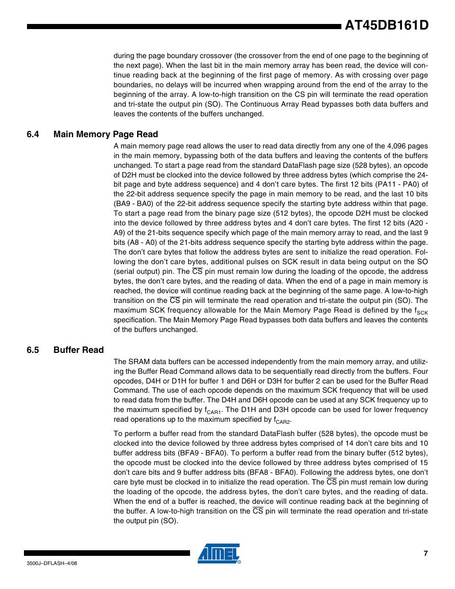
6.4 Main Memory Page Read
A main memory page read allows the user to read data directly from any one of the 4,096 pages
in the main memory, bypassing both of the data buffers and leaving the contents of the buffers
unchanged. To start a page read from the standard DataFlash page size (528 bytes), an opcode
of D2H must be clocked into the device followed by three address bytes (which comprise the 24-
bit page and byte address sequence) and 4 don’t care bytes. The first 12 bits (PA11 - PA0) of
the 22-bit address sequence specify the page in main memory to be read, and the last 10 bits
(BA9 - BA0) of the 22-bit address sequence specify the starting byte address within that page.
To start a page read from the binary page size (512 bytes), the opcode D2H must be clocked
into the device followed by three address bytes and 4 don’t care bytes. The first 12 bits (A20 -
A9) of the 21-bits sequence specify which page of the main memory array to read, and the last 9
bits (A8 - A0) of the 21-bits address sequence specify the starting byte address within the page.
The don’t care bytes that follow the address bytes are sent to initialize the read operation. Fol-
lowing the don’t care bytes, additional pulses on SCK result in data being output on the SO
(serial output) pin. The CS pin must remain low during the loading of the opcode, the address
bytes, the don’t care bytes, and the reading of data. When the end of a page in main memory is
reached, the device will continue reading back at the beginning of the same page. A low-to-high
transition on the CS pin will terminate the read operation and tri-state the output pin (SO). The
maximum SCK frequency allowable for the Main Memory Page Read is defined by the fSCK
specification. The Main Memory Page Read bypasses both data buffers and leaves the contents
of the buffers unchanged.
The SRAM data buffers can be accessed independently from the main memory array, and utiliz-
ing the Buffer Read Command allows data to be sequentially read directly from the buffers. Four
opcodes, D4H or D1H for buffer 1 and D6H or D3H for buffer 2 can be used for the Buffer Read
Command. The use of each opcode depends on the maximum SCK frequency that will be used
to read data from the buffer. The D4H and D6H opcode can be used at any SCK frequency up to
the maximum specified by fCAR1. The D1H and D3H opcode can be used for lower frequency
read operations up to the maximum specified by fCAR2.
To perform a buffer read from the standard DataFlash buffer (528 bytes), the opcode must be
clocked into the device followed by three address bytes comprised of 14 don’t care bits and 10
buffer address bits (BFA9 - BFA0). To perform a buffer read from the binary buffer (512 bytes),
the opcode must be clocked into the device followed by three address bytes comprised of 15
don’t care bits and 9 buffer address bits (BFA8 - BFA0). Following the address bytes, one don’t
care byte must be clocked in to initialize the read operation. The CS pin must remain low during
the loading of the opcode, the address bytes, the don’t care bytes, and the reading of data.
When the end of a buffer is reached, the device will continue reading back at the beginning of
the buffer. A low-to-high transition on the CS pin will terminate the read operation and tri-state
the output pin (SO).
6.5
Buffer Read
3500J–DFLASH–4/08
7
�
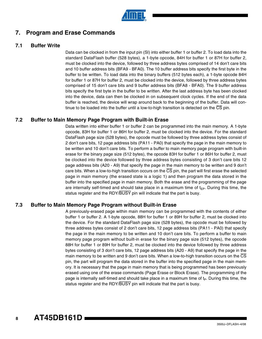
7. Program and Erase Commands
7.1
Buffer Write
Data can be clocked in from the input pin (SI) into either buffer 1 or buffer 2. To load data into the
standard DataFlash buffer (528 bytes), a 1-byte opcode, 84H for buffer 1 or 87H for buffer 2,
must be clocked into the device, followed by three address bytes comprised of 14 don’t care bits
and 10 buffer address bits (BFA9 - BFA0). The 10 buffer address bits specify the first byte in the
buffer to be written. To load data into the binary buffers (512 bytes each), a 1-byte opcode 84H
for buffer 1 or 87H for buffer 2, must be clocked into the device, followed by three address bytes
comprised of 15 don’t care bits and 9 buffer address bits (BFA8 - BFA0). The 9 buffer address
bits specify the first byte in the buffer to be written. After the last address byte has been clocked
into the device, data can then be clocked in on subsequent clock cycles. If the end of the data
buffer is reached, the device will wrap around back to the beginning of the buffer. Data will con-
tinue to be loaded into the buffer until a low-to-high transition is detected on the CS pin.
7.2
Buffer to Main Memory Page Program with Built-in Erase
Data written into either buffer 1 or buffer 2 can be programmed into the main memory. A 1-byte
opcode, 83H for buffer 1 or 86H for buffer 2, must be clocked into the device. For the standard
DataFlash page size (528 bytes), the opcode must be followed by three address bytes consist of
2 don’t care bits, 12 page address bits (PA11 - PA0) that specify the page in the main memory to
be written and 10 don’t care bits. To perform a buffer to main memory page program with built-in
erase for the binary page size (512 bytes), the opcode 83H for buffer 1 or 86H for buffer 2, must
be clocked into the device followed by three address bytes consisting of 3 don’t care bits 12
page address bits (A20 - A9) that specify the page in the main memory to be written and 9 don’t
care bits. When a low-to-high transition occurs on the CS pin, the part will first erase the selected
page in main memory (the erased state is a logic 1) and then program the data stored in the
buffer into the specified page in main memory. Both the erase and the programming of the page
are internally self-timed and should take place in a maximum time of tEP. During this time, the
status register and the RDY/BUSY pin will indicate that the part is busy.
7.3
Buffer to Main Memory Page Program without Built-in Erase
A previously-erased page within main memory can be programmed with the contents of either
buffer 1 or buffer 2. A 1-byte opcode, 88H for buffer 1 or 89H for buffer 2, must be clocked into
the device. For the standard DataFlash page size (528 bytes), the opcode must be followed by
three address bytes consist of 2 don’t care bits, 12 page address bits (PA11 - PA0) that specify
the page in the main memory to be written and 10 don’t care bits. To perform a buffer to main
memory page program without built-in erase for the binary page size (512 bytes), the opcode
88H for buffer 1 or 89H for buffer 2, must be clocked into the device followed by three address
bytes consisting of 3 don’t care bits, 12 page address bits (A20 - A9) that specify the page in the
main memory to be written and 9 don’t care bits. When a low-to-high transition occurs on the CS
pin, the part will program the data stored in the buffer into the specified page in the main mem-
ory. It is necessary that the page in main memory that is being programmed has been previously
erased using one of the erase commands (Page Erase or Block Erase). The programming of the
page is internally self-timed and should take place in a maximum time of tP. During this time, the
status register and the RDY/BUSY pin will indicate that the part is busy.
8
AT45DB161D
3500J–DFLASH–4/08
�


 V2版本原理图(Capacitive-Fingerprint-Reader-Schematic_V2).pdf
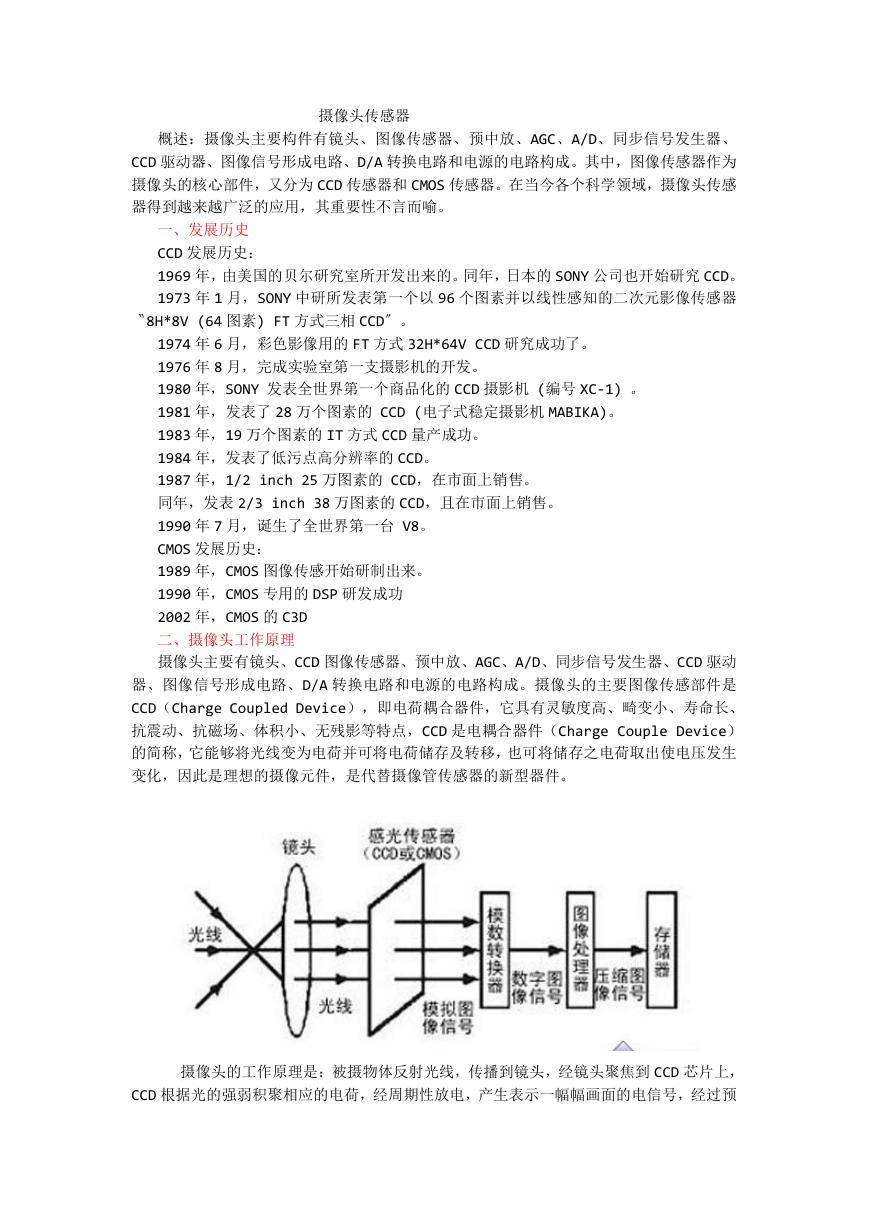 摄像头工作原理.doc
 VL53L0X简要说明(En.FLVL53L00216).pdf
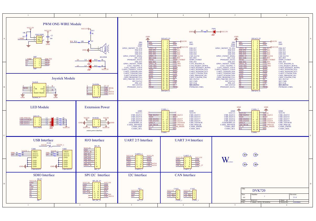 原理图(DVK720-Schematic).pdf
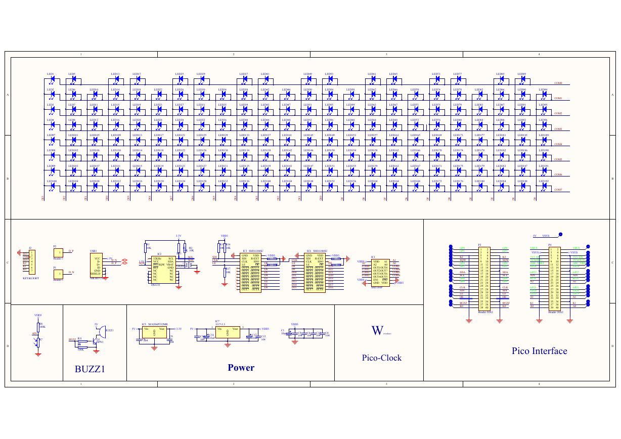 原理图(Pico-Clock-Green-Schdoc).pdf
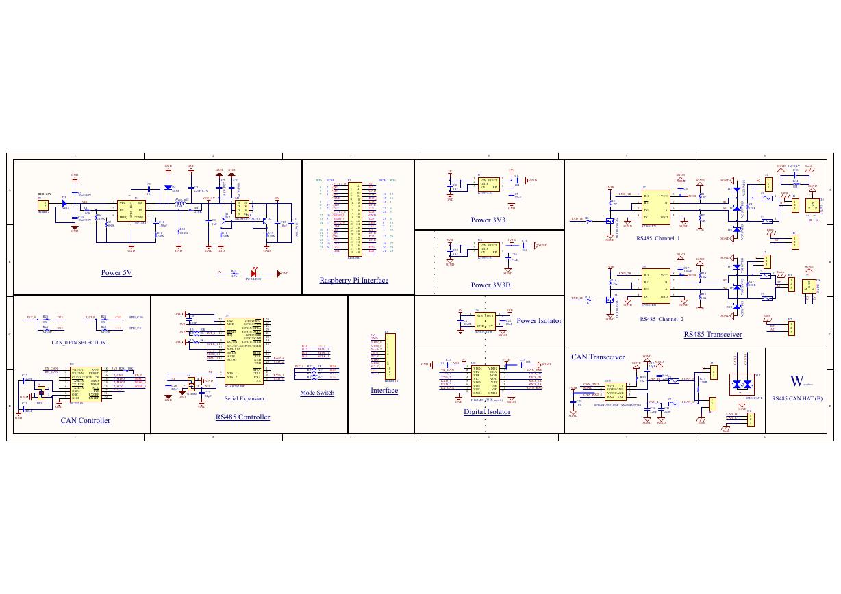 原理图(RS485-CAN-HAT-B-schematic).pdf
 File:SIM7500_SIM7600_SIM7800 Series_SSL_Application Note_V2.00.pdf
 ADS1263(Ads1262).pdf
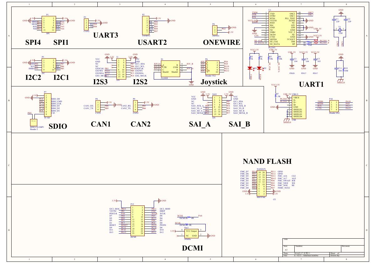 原理图(Open429Z-D-Schematic).pdf
 用户手册(Capacitive_Fingerprint_Reader_User_Manual_CN).pdf
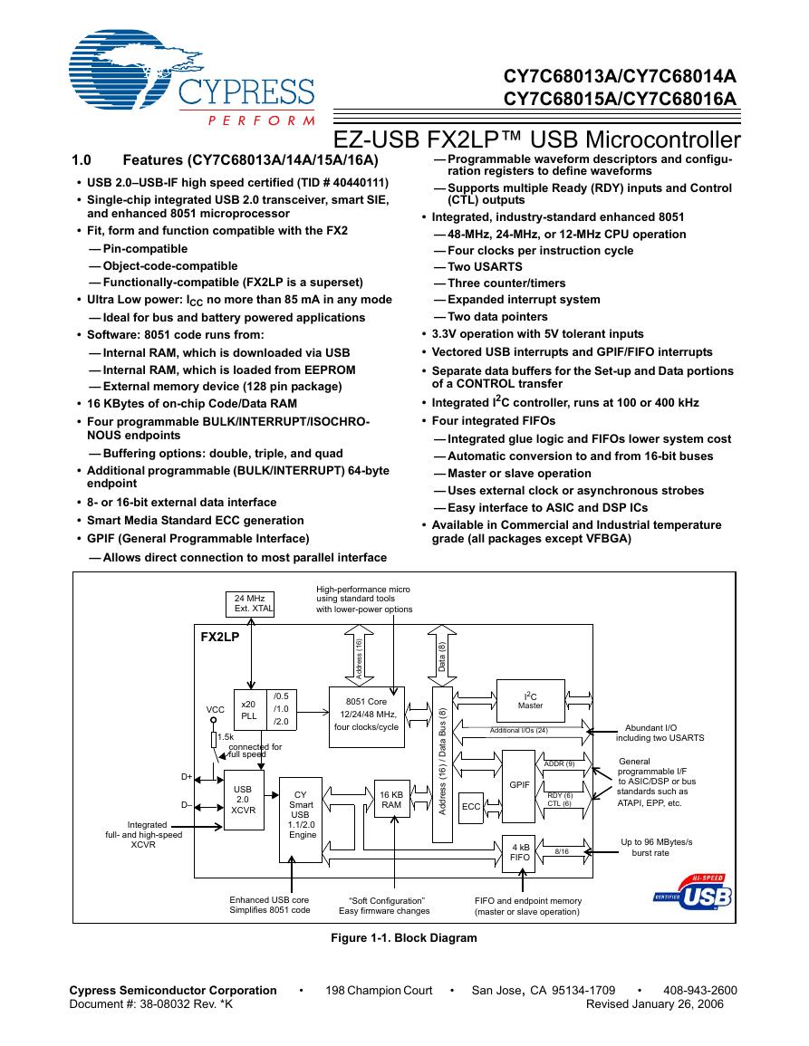 CY7C68013A(英文版)(CY7C68013A).pdf
 TechnicalReference_Dem.pdf