UM1793
User manual
Dynamic NFC tag expansion board based on M24SR
for STM32 Nucleo
Introduction
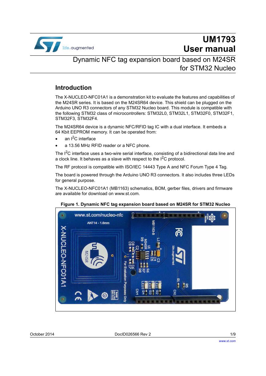
The X-NUCLEO-NFC01A1 is a demonstration kit to evaluate the features and capabilities of
the M24SR series. It is based on the M24SR64 device. This shield can be plugged on the
Arduino UNO R3 connectors of any STM32 Nucleo board. This module is compatible with
the following STM32 class of microcontrollers: STM32L0, STM32L1, STM32F0, STM32F1,
STM32F3, STM32F4.
The M24SR64 device is a dynamic NFC/RFID tag IC with a dual interface. It embeds a
64 Kbit EEPROM memory. It can be operated from:
•
•
The I2C interface uses a two-wire serial interface, consisting of a bidirectional data line and
a clock line. It behaves as a slave with respect to the I2C protocol.
The RF protocol is compatible with ISO/IEC 14443 Type A and NFC Forum Type 4 Tag.
The board is powered through the Arduino UNO R3 connectors. It also includes three LEDs
for general purpose.
The X-NUCLEO-NFC01A1 (MB1163) schematics, BOM, gerber files, drivers and firmware
are available for download on www.st.com.
an I2C interface
a 13.56 MHz RFID reader or a NFC phone.
Figure 1. Dynamic NFC tag expansion board based on M24SR for STM32 Nucleo
October 2014
DocID026566 Rev 2
1/9
www.st.com
9
�
Description
1
Description
UM1793
The X-NUCLEO-NFC01A1 board contains the M24SR64-Y chip. It is a dynamic NFC/RFID
tag IC. It features a 64 Kbit EEPROM memory, preformatted for NFC transactions, and
which can be protected by a unique and flexible 128-bit password scheme. The memory
bank can be accessed by any of its two interfaces, either from an I2C interface or by a
13.56 MHz passive NFC interface. The I2C interface is a two-wire serial interface, consisting
of a bidirectional data line and a clock line. It behaves as a slave with respect to the I2C
protocol. The NFC interface is based on the ISO/IEC 14443 type A and NFC Forum type 4
tag specifications. Because it is a passive RF interface, it operates when the board is
powered on but also when the board is powered off. Two control pins are also available from
the M24SR64-Y chip, allowing flexible management of the NFC interface.
2/9
DocID026566 Rev 2
�
UM1793
2
Features
Features
Ready-to-use printed circuit board (PCB) including:
•
•
M24SR64-Y dynamic NFC/RFID tag
31 mm x 30 mm 13.56 MHz double layer inductive antenna etched on the PCB
(ANT14)
Different color LEDs
Arduino UNO R3 connectors for Nucleo Board.
•
•
DocID026566 Rev 2
3/9
9
�
Hardware and layout description
UM1793
3
Hardware and layout description
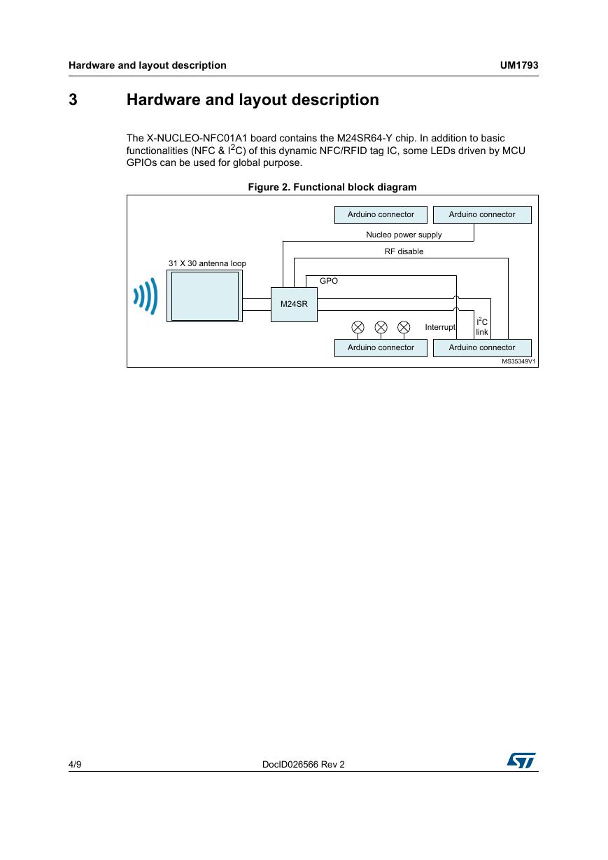
The X-NUCLEO-NFC01A1 board contains the M24SR64-Y chip. In addition to basic
functionalities (NFC & I2C) of this dynamic NFC/RFID tag IC, some LEDs driven by MCU
GPIOs can be used for global purpose.
Figure 2. Functional block diagram
4/9
DocID026566 Rev 2
�
UM1793
Hardware and layout description
3.1
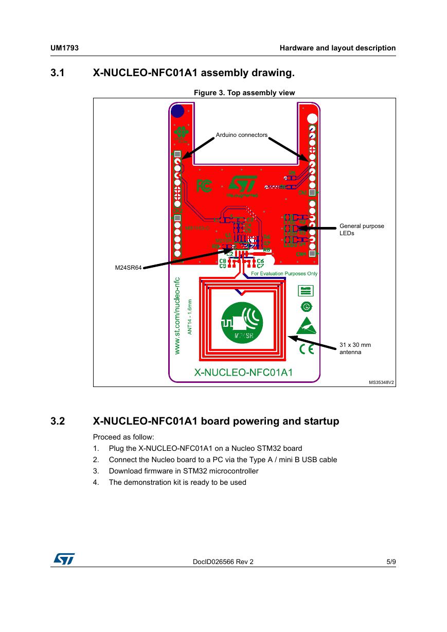
X-NUCLEO-NFC01A1 assembly drawing.
Figure 3. Top assembly view
3.2
X-NUCLEO-NFC01A1 board powering and startup
Proceed as follow:
1. Plug the X-NUCLEO-NFC01A1 on a Nucleo STM32 board
2. Connect the Nucleo board to a PC via the Type A / mini B USB cable
3. Download firmware in STM32 microcontroller
4. The demonstration kit is ready to be used
DocID026566 Rev 2
5/9
9
�
4
6
9
/
Electrical schematics
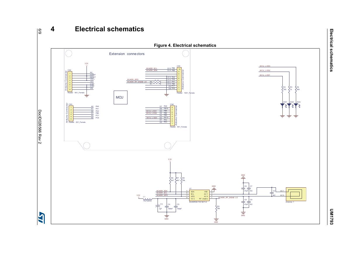
Figure 4. Electrical schematics
D
o
c
I
D
0
2
6
5
6
6
R
e
v
2
l
E
e
c
t
r
i
c
a
l
s
c
h
e
m
a
t
i
c
s
U
M
1
7
9
3
�
UM1793
5
5.1
An overview of FCC regulations
An overview of FCC regulations
Part 15.105
This equipment has been tested and found to comply with the limits for a Class B digital
device, pursuant to part 15 of the FCC Rules. These limits are designed to provide
reasonable protection against harmful interference in a residential installation. This
equipment generates uses and can radiate radio frequency energy and, if not installed and
used in accordance with the instructions, may cause harmful interference to radio
communications. However, there is no guarantee that interference will not occur in a
particular installation. If this equipment does cause harmful interference to radio or
television reception, which can be determined by turning the equipment off and on, the user
is encouraged to try to correct the interference's by one or more of the following measures:
•
•
•
Reorient or relocate the receiving antenna.
Increase the separation between the equipment and the receiver.
Connect the equipment into an outlet on a circuit different from that to which the
receiver is connected.
Consult the dealer or an experienced radio/TV technician for help.
•
5.2
Part 15.21
Any changes or modifications to this equipment not expressly approved by
STMicroelectronics may cause, harmful interference and void the FCC authorization to
operate this equipment.
DocID026566 Rev 2
7/9
9
�
Revision history
6
Revision history
UM1793
Date
19-Jun-2014
31-Oct-2014
Table 1. Document revision history
Revision
Changes
1
2
Initial release.
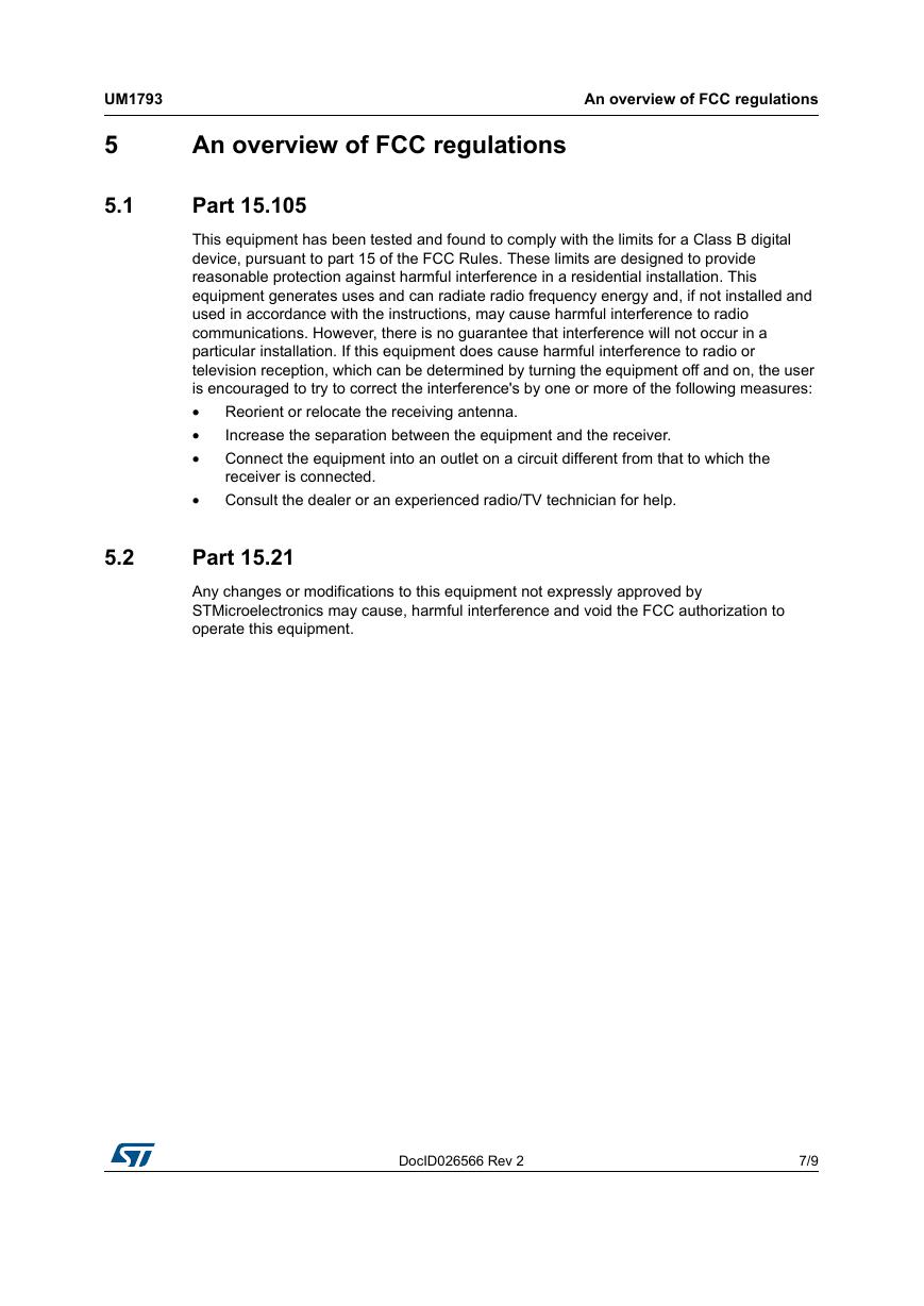
Updated Figure 1: Dynamic NFC tag expansion board
based on M24SR for STM32 Nucleo.
Updated Figure 3: Top assembly view.
Updated Figure 4: Electrical schematics.
Added Section 5: An overview of FCC regulations.
8/9
DocID026566 Rev 2
�




 V2版本原理图(Capacitive-Fingerprint-Reader-Schematic_V2).pdf
 摄像头工作原理.doc
 VL53L0X简要说明(En.FLVL53L00216).pdf
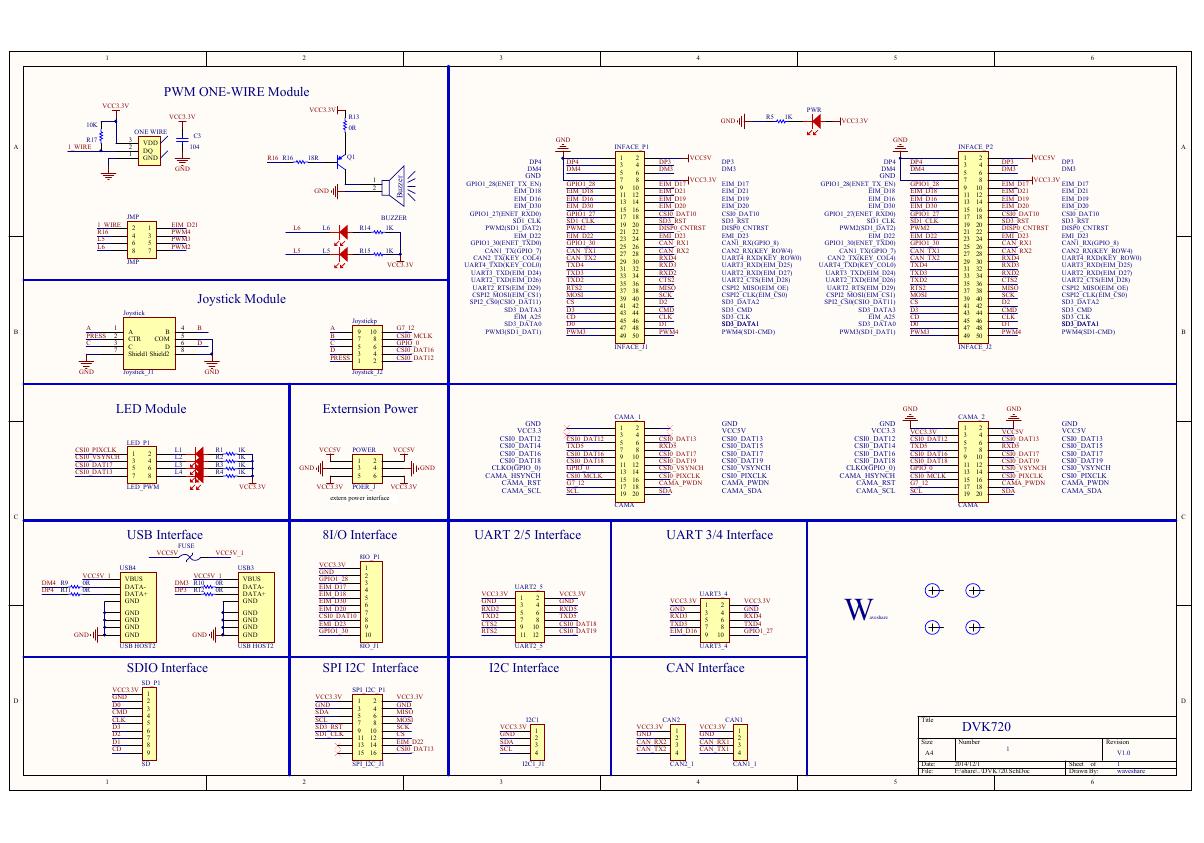 原理图(DVK720-Schematic).pdf
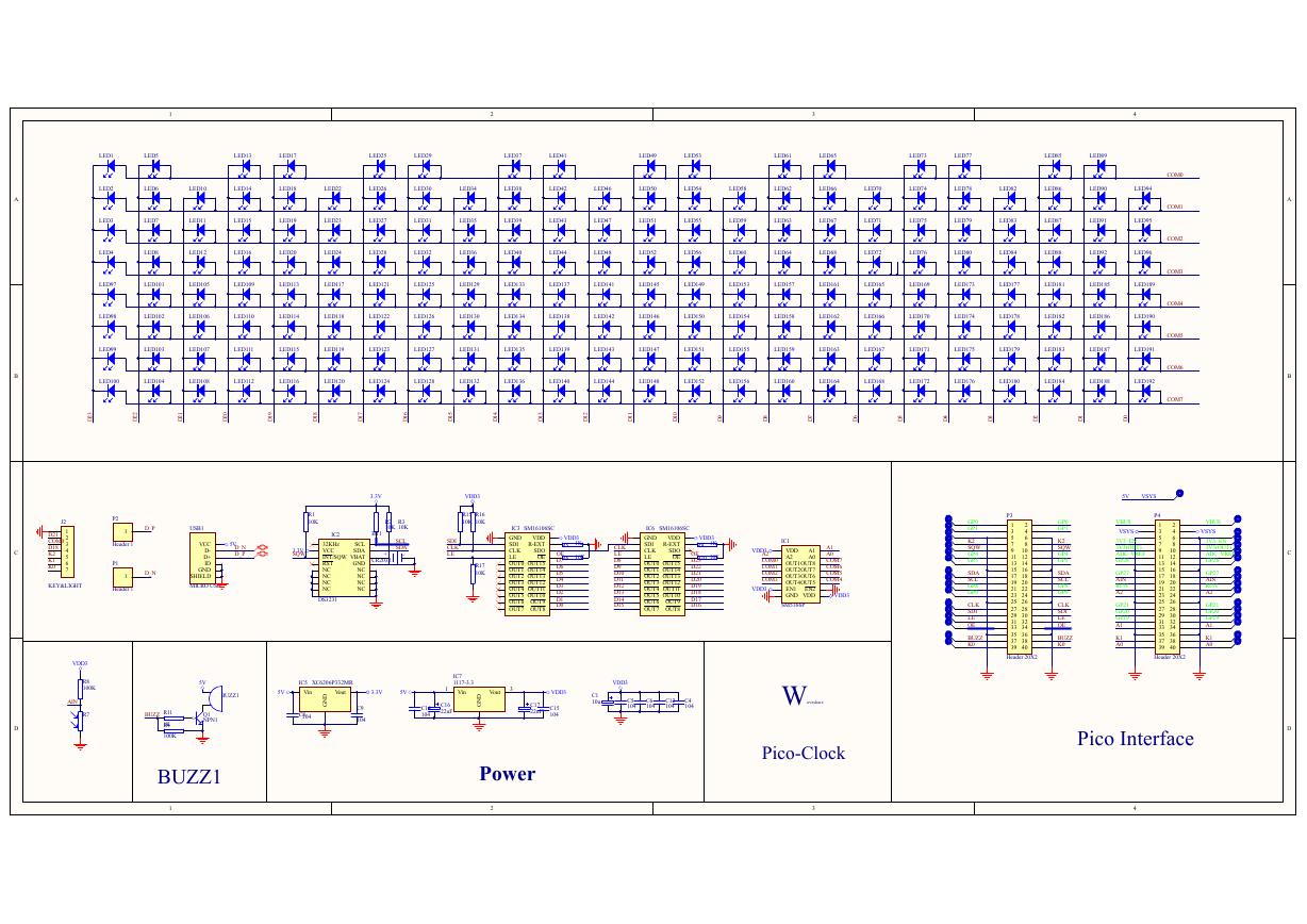 原理图(Pico-Clock-Green-Schdoc).pdf
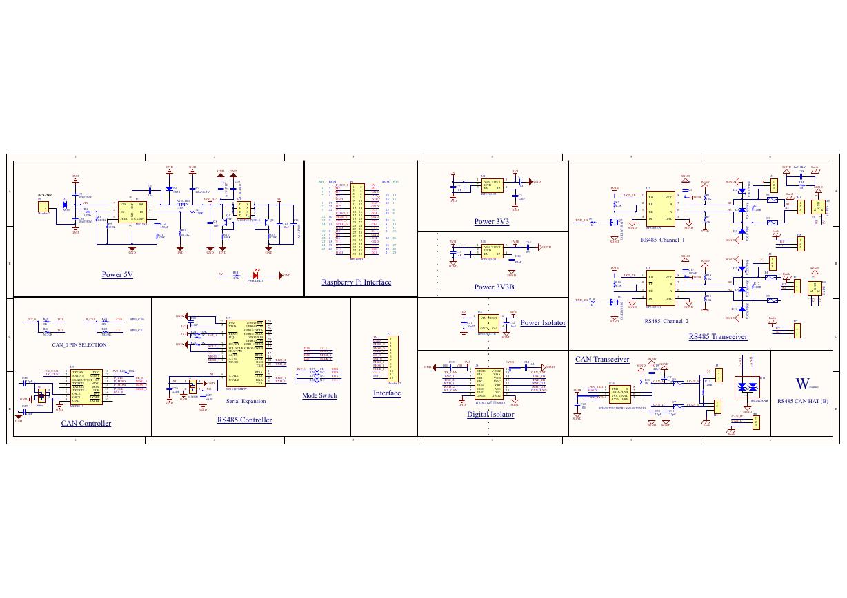 原理图(RS485-CAN-HAT-B-schematic).pdf
 File:SIM7500_SIM7600_SIM7800 Series_SSL_Application Note_V2.00.pdf
 ADS1263(Ads1262).pdf
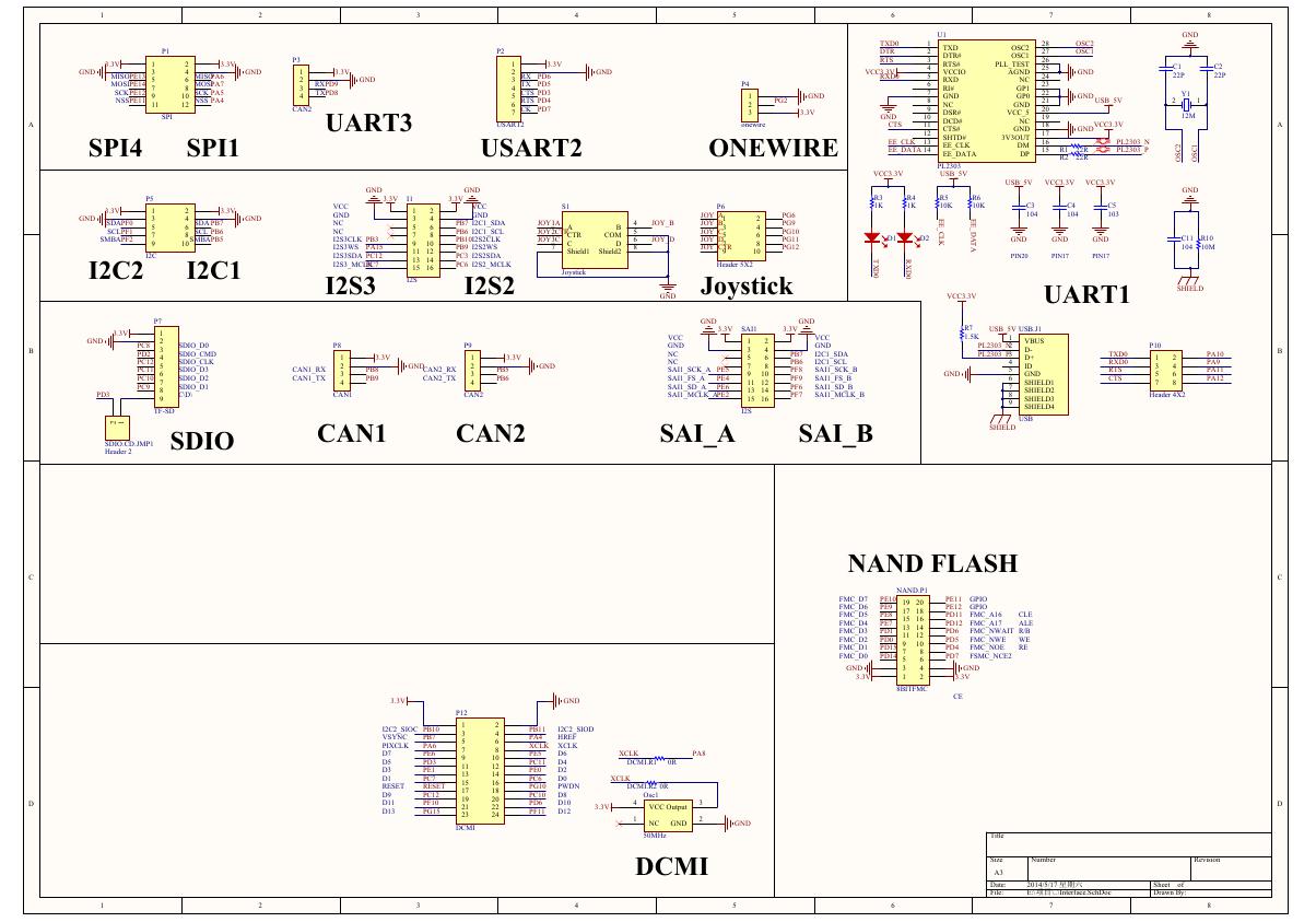 原理图(Open429Z-D-Schematic).pdf
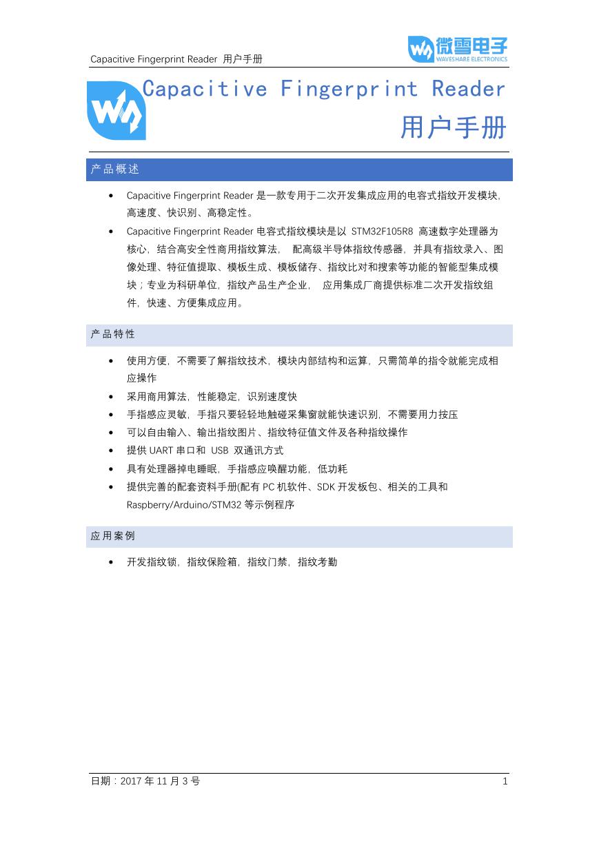 用户手册(Capacitive_Fingerprint_Reader_User_Manual_CN).pdf
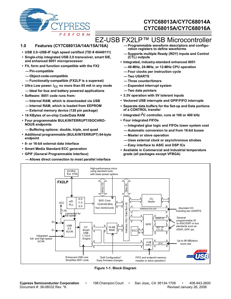 CY7C68013A(英文版)(CY7C68013A).pdf
 TechnicalReference_Dem.pdf