PN532/C1
NFC controller
Rev. 1.2 — 31 March 2011
Short form data sheet
1.
Introduction
This document describes the NFC controller PN532. This document is a short form
version; for full specification refer to the product data sheet.
2. General description
The PN532 is a highly integrated transmission module for contactless communication at
13.56 MHZ including micro-controller functionality based on an 80C51 core. The
transmission module utilises an outstanding modulation and demodulation concept
completely integrated for different kinds of passive contactless communication methods
and protocols at 13.56 MHZ.
The PN532 support 4 different operating modes:
• Reader/writer mode supporting ISO 14443A / MIFARE® and FeliCa™ scheme
ISO 14443B in reader/writer mode only.
Card interface mode supporting ISO 14443A / MIFARE® and FeliCa™ scheme
NFCIP-1 mode
Enabled in reader/ writer mode for ISO reader 14443A / MIFARE® and reader/writer mode
for ISO 14443B, the PN532’s internal transmitter part is able to drive a reader/writer
antenna designed to communicate with ISO14443A /MIFARE® and ISO14443B cards and
transponders without additional active circuitry.
The receiver part provides a robust and efficient implementation of a demodulation and
decoding circuitry for signals from ISO 14443A / MIFARE® and ISO 14443B compatible
cards and transponders. The digital part handles the complete ISO14443A framing and
error detection (Parity & CRC).
The PN532 supports MIFARE“ Classic (e.g. MIFARE® Standard) products. The PN532
supports contactless communication using MIFARE® Higher Baudrates up to 424kBaud in
both directions.
Enabled in the reader/ writer mode for FeliCa™, the PN532 transmission module supports
the FeliCa™ communication scheme. The receiver part provides a robust and efficient
implementation of the demodulation and decoding circuitry for FeliCa™ coded signals.
The digital part handles the FeliCa™ framing and error detection like CRC. The PN532
supports contactless communication using FeliCa™ Higher Baudrates up to 424 kbaud in
both directions.
�
Philips Semiconductors
PN532/C1
NFC controller
3. Features
Enabled in card mode the PN532 transmission module is able to answer to a reader/writer
command either acoording to FeliCa™ or ISO14443 A / MIFARE® card interface mode.
The PN532 generates the digital load-modulated signals and in addition with an external
circuit the answers can be send back to the reader/writer. A complete card functionality is
only possible in combination with a secure memory IC.
Additionally, the PN532 transmission module offers the possibility to communicate directly
to a second NFCIP-1 device in the NFCIP-1 mode. The NFCIP-1 mode offers different
communication transfer speeds up to 424 kbit/s according to the ECMA 340 NFCIP-1
Standard. The digital part handles the complete NFCIP-1 framing and error detection.
Transfer speeds on the RF interface above 424 kbit/s are supported by the digital part of
the PN532 module. The modulation to transmit and the demodulation to receive data at
transfer speeds has than to be done by an external circuit.
To make information exchange to the host systems several interfaces are implemented:
SPI interface
I2C interface
Serial UART (similar to RS232 with 0 and PVDD voltage levels)
The PN532 embeds a low dropout voltage regulator allowing the device to be connected
directly to a battery as well as a medium power switch to supply and control the power of
the companion secure chip.
80C51 micro controller core with 40 kbyte ROM and 1 kbyte RAM
Highly integrated analog circuitry to demodulate and decode responses
Buffered output drivers to connect an antenna with minimum number of external
components
Integrated RF Level detector
Integrated data mode detector
Supports ISO 14443A / MIFARE®
Supports ISO 14443B in reader/writer mode only
Typical operating distance in reader/writer mode for communication to a
ISO14443A/MIFARE®, ISO14443B or FeliCa™ card up to 50 mm depending on the
antenna size and tuning
Typical operating distance in NFCIP-1 mode up to 50 mm depending on the antenna
size and tuning and power supply
Typical operating distance in ISO14443A / MIFARE® card or FeliCa™ card interface
mode of about 100 mm depending on the antenna size and tuning and the external
field strength
Supports MIFARE® Classic encryption in reader/writer mode and MIFARE® higher
transfer speed communication at 212 kbit/s and 424 kbit/s
Supports contactless communication according to the FeliCa™ scheme at 212 kbaud
and 424 kbaud
Integrated RF interface for NFCIP-1 up to 424 kBaud
Possibility to communicate on the RF interface above 424 kbaud using external
analog circuitry
9397 750 XXXXX
Short form data sheet
Rev. 1.2 — 31 March 2011
© Koninklijke Philips Electronics N.V. 2006. All rights reserved.
2 of 25
�
Philips Semiconductors
PN532/C1
NFC controller
Supported host interfaces
SPI interface
I2C interface
High Speed Serial UART (similar to RS232 with 0 and PVDD voltage levels)
Flexible interrupt using IRQ pin
Hard reset with low power function
Power down mode per embedded firmware
Automatic wake up on the I2C, HSU and SPI interfaces when device is in power down
mode
Programmable timer
Internal oscillator to connect 27.12 MHz crystal
2.7 to 5.4V power supply
Power Switch for external secure companion chip.
Specific IO ports for external devices control
Embedded test of absence of antenna and/or antenna tuning components by detection
of significant load impedance deviation resulting in high power consumption increase.
4. Applications
Mobile and portable devices
PC world
Consumer application
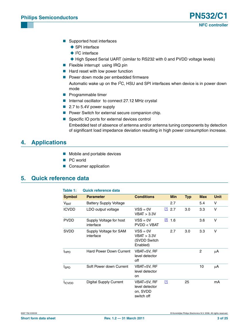
5. Quick reference data
Table 1:
Symbol
VBAT
ICVDD
PVDD
SVDD
IHPD
ISPD
IICVDD
Quick reference data
Parameter
Battery Supply Voltage
LDO output voltage
Supply Voltage for host
interface
Supply Voltage for SAM
interface
Conditions
VSS = 0V
VBAT > 3.3V
VSS = 0V
PVDD < VBAT
VSS = 0V
VBAT > 3.3V
(SVDD Switch
Enabled)
Soft Power down Current
Hard Power Down Current VBAT=5V, RF
level detector
off
VBAT=5V, RF
level detector
on
VBAT=5V, RF
level detector
on, SVDD
switch off
Digital Supply Current
Typ
3.0
Min
2.7
[1] 2.7
[2] 1.6
2.7
3.0
Max
5.4
3.3
3.6
3.3
Unit
V
V
V
V
2
μA
10
μA
[1]
25
mA
9397 750 XXXXX
Short form data sheet
Rev. 1.2 — 31 March 2011
© Koninklijke Philips Electronics N.V. 2006. All rights reserved.
3 of 25
�
Philips Semiconductors
Table 1:
Symbol
ISVDD
PN532/C1
NFC controller
Quick reference data …continued
Parameter
SVDD Supply Current
IAVDD
Analog Supply Current
ITVDD
IVBAT
Transmitter (TX) Supply
Current
continuous total current
consumption
Min
Typ
Max
30
Unit
mA
6
mA
60
100
mA
91
140
mA
Conditions
VBAT=5V,
SVDD switch
on
IVBAT=5V, RF
level detector
on
During RF
VBAT=5V, 40Ω
typical TX Zload
(min. tbd)
Tamb = -30 to +
85 °C, 40Ω
typical TX Zload
(min tbd),
excluding the
secure
companion chip
[1]
[1]
[3]
Tamb
operating ambient
temperature
-30
+85
°C
[1] DVDD, AVDD and TVDD shall always be connected together.
[2]
It is not allowed to have PVDD above VBAT
[3] The total current consumption depends also on the firmware version (different internal IC clock speed)
6. Ordering information
Table 2:
Type number
Ordering information
Package
Name
Description
PN5320A3HN/C101 [1] HVQFN40 plastic, heatsink very thin quad flat package; no leads; 40terminals;
body 6x 6x 0.85mm
Version
SOT618-1
PN5321A3HN/C101 [2] HVQFN40 plastic, heatsink very thin quad flat package; no leads; 40terminals;
SOT618-1
body 6x 6x 0.85mm. Type B SW is enable.
[1]
01 is the reference of the romcode version.
[2] A purchaser of this Philips IC has to take care for appropriate third party patent license.
9397 750 XXXXX
Short form data sheet
Rev. 1.2 — 31 March 2011
© Koninklijke Philips Electronics N.V. 2006. All rights reserved.
4 of 25
�
Philips Semiconductors
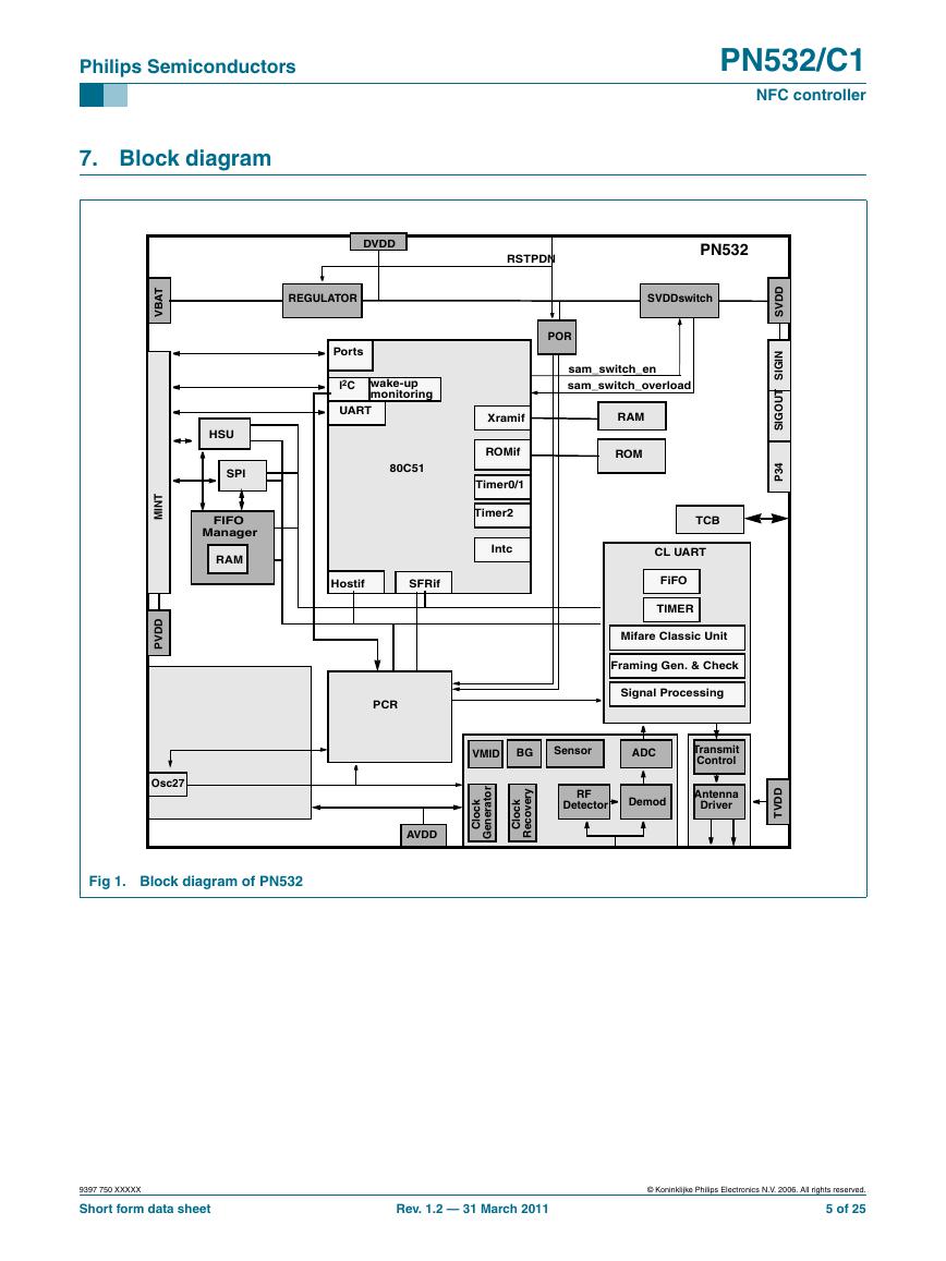
7. Block diagram
PN532/C1
NFC controller
T
A
B
V
T
N
M
I
D
D
V
P
Osc27
DVDD
RSTPDN
PN532
REGULATOR
SVDDswitch
D
D
V
S
Ports
I2C
wake-up
monitoring
UART
80C51
Hostif
SFRif
Xramif
ROMif
Timer0/1
Timer2
Intc
HSU
SPI
FIFO
Manager
RAM
I
N
G
S
I
T
U
O
G
S
I
4
3
P
POR
sam_switch_en
sam_switch_overload
RAM
ROM
TCB
CL UART
FiFO
TIMER
Mifare Classic Unit
Framing Gen. & Check
Signal Processing
PCR
AVDD
VMID BG
Sensor
ADC
Transmit
Control
k
c
o
C
l
r
o
t
a
r
e
n
e
G
RF
Detector
Demod
Antenna
Driver
D
D
V
T
k
c
o
C
l
y
r
e
v
o
c
e
R
Fig 1. Block diagram of PN532
9397 750 XXXXX
Short form data sheet
Rev. 1.2 — 31 March 2011
© Koninklijke Philips Electronics N.V. 2006. All rights reserved.
5 of 25
�
Philips Semiconductors
8. Pinning information
PN532/C1
NFC controller
8.1 Pin description
PN532 Pin description
Pin Type Pad Ref
Voltage
Description
1
2
3
4
5
6
7
8
9
10
11
12
13
14
15
16
17
18
19
20
21
22
23
24
25
26
27
28
29
30
PWR
O
PWR
O
PWR
O
PWR
PWR
O
I
PWR
O
O
I
O
I
I
I
DVDD
TVDD
TVDD
AVDD
AVDD
AVDD
AVDD
AVDD
AVDD
DVDD
DVDD
DVDD
IO
DVDD
PWR
IO
PVDD
O
IO
IO
IO
IO
IO
PVDD
PVDD
PVDD
PVDD
PVDD
PVDD
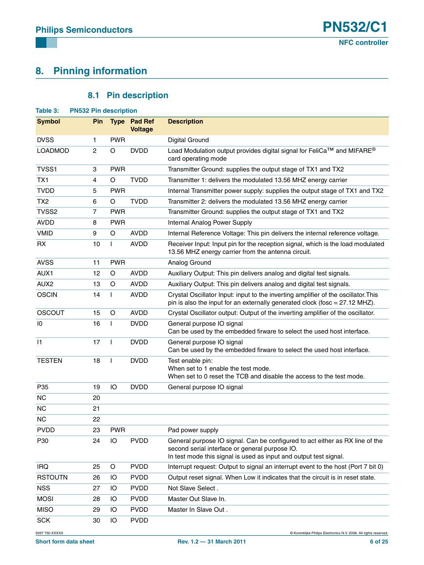
Digital Ground
Load Modulation output provides digital signal for FeliCa™ and MIFARE®
card operating mode
Transmitter Ground: supplies the output stage of TX1 and TX2
Transmitter 1: delivers the modulated 13.56 MHZ energy carrier
Internal Transmitter power supply: supplies the output stage of TX1 and TX2
Transmitter 2: delivers the modulated 13.56 MHZ energy carrier
Transmitter Ground: supplies the output stage of TX1 and TX2
Internal Analog Power Supply
Internal Reference Voltage: This pin delivers the internal reference voltage.
Receiver Input: Input pin for the reception signal, which is the load modulated
13.56 MHZ energy carrier from the antenna circuit.
Analog Ground
Auxiliary Output: This pin delivers analog and digital test signals.
Auxiliary Output: This pin delivers analog and digital test signals.
Crystal Oscillator Input: input to the inverting amplifier of the oscillator.This
pin is also the input for an externally generated clock (fosc = 27.12 MHZ).
Crystal Oscillator output: Output of the inverting amplifier of the oscillator.
General purpose IO signal
Can be used by the embedded firware to select the used host interface.
General purpose IO signal
Can be used by the embedded firware to select the used host interface.
Test enable pin:
When set to 1 enable the test mode.
When set to 0 reset the TCB and disable the access to the test mode.
General purpose IO signal
Pad power supply
General purpose IO signal. Can be configured to act either as RX line of the
second serial interface or general purpose IO.
In test mode this signal is used as input and output test signal.
Interrupt request: Output to signal an interrupt event to the host (Port 7 bit 0)
Output reset signal. When Low it indicates that the circuit is in reset state.
Not Slave Select .
Master Out Slave In.
Master In Slave Out .
Table 3:
Symbol
DVSS
LOADMOD
TVSS1
TX1
TVDD
TX2
TVSS2
AVDD
VMID
RX
AVSS
AUX1
AUX2
OSCIN
OSCOUT
I0
I1
TESTEN
P35
NC
NC
NC
PVDD
P30
IRQ
RSTOUTN
NSS
MOSI
MISO
SCK
9397 750 XXXXX
Short form data sheet
Rev. 1.2 — 31 March 2011
© Koninklijke Philips Electronics N.V. 2006. All rights reserved.
6 of 25
�
Philips Semiconductors
PN532/C1
NFC controller
PN532 Pin description …continued
Table 3:
Symbol
P31
Pin Type Pad Ref
Voltage
PVDD
31
IO
P32_INT0
32
IO
PVDD
P33_INT1
33
IO
PVDD
P34
SIGOUT
34
35
IO
O
SVDD
SVDD
SIGIN
36
I
SVDD
SVDD
37
O
RSTPDN
38
I
PVDD
DVDD
VBAT
39
40
PWR
PWR
Description
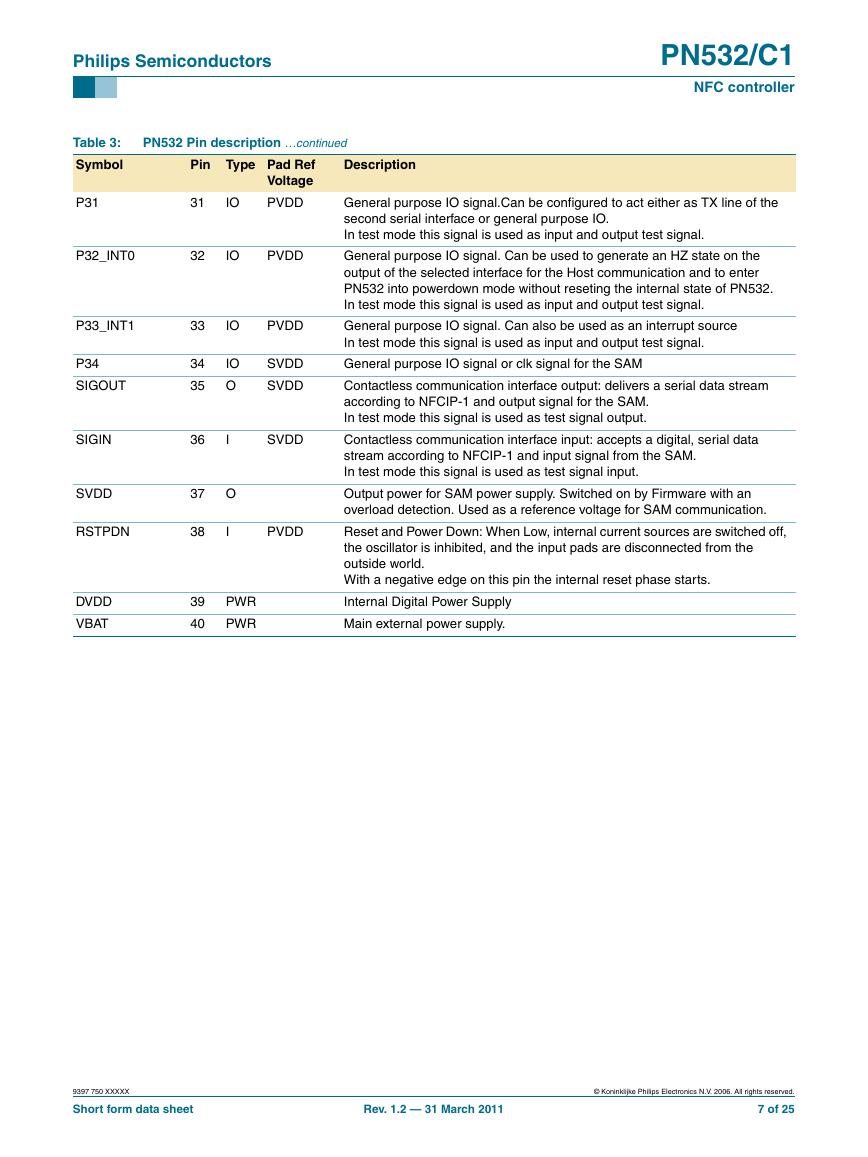
General purpose IO signal.Can be configured to act either as TX line of the
second serial interface or general purpose IO.
In test mode this signal is used as input and output test signal.
General purpose IO signal. Can be used to generate an HZ state on the
output of the selected interface for the Host communication and to enter
PN532 into powerdown mode without reseting the internal state of PN532.
In test mode this signal is used as input and output test signal.
General purpose IO signal. Can also be used as an interrupt source
In test mode this signal is used as input and output test signal.
General purpose IO signal or clk signal for the SAM
Contactless communication interface output: delivers a serial data stream
according to NFCIP-1 and output signal for the SAM.
In test mode this signal is used as test signal output.
Contactless communication interface input: accepts a digital, serial data
stream according to NFCIP-1 and input signal from the SAM.
In test mode this signal is used as test signal input.
Output power for SAM power supply. Switched on by Firmware with an
overload detection. Used as a reference voltage for SAM communication.
Reset and Power Down: When Low, internal current sources are switched off,
the oscillator is inhibited, and the input pads are disconnected from the
outside world.
With a negative edge on this pin the internal reset phase starts.
Internal Digital Power Supply
Main external power supply.
9397 750 XXXXX
Short form data sheet
Rev. 1.2 — 31 March 2011
© Koninklijke Philips Electronics N.V. 2006. All rights reserved.
7 of 25
�
Philips Semiconductors
9. Functional description
9.1 CONTACT LESS MODULE
PN532/C1
NFC controller
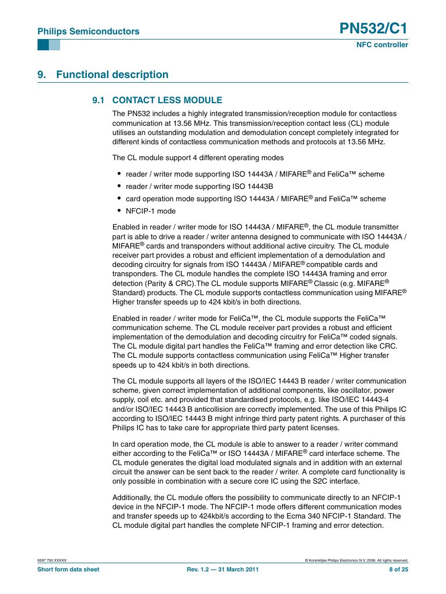
The PN532 includes a highly integrated transmission/reception module for contactless
communication at 13.56 MHz. This transmission/reception contact less (CL) module
utilises an outstanding modulation and demodulation concept completely integrated for
different kinds of contactless communication methods and protocols at 13.56 MHz.
The CL module support 4 different operating modes
reader / writer mode supporting ISO 14443A / MIFARE® and FeliCa™ scheme
reader / writer mode supporting ISO 14443B
card operation mode supporting ISO 14443A / MIFARE® and FeliCa™ scheme
NFCIP-1 mode
Enabled in reader / writer mode for ISO 14443A / MIFARE®, the CL module transmitter
part is able to drive a reader / writer antenna designed to communicate with ISO 14443A /
MIFARE® cards and transponders without additional active circuitry. The CL module
receiver part provides a robust and efficient implementation of a demodulation and
decoding circuitry for signals from ISO 14443A / MIFARE® compatible cards and
transponders. The CL module handles the complete ISO 14443A framing and error
detection (Parity & CRC).The CL module supports MIFARE® Classic (e.g. MIFARE®
Standard) products. The CL module supports contactless communication using MIFARE®
Higher transfer speeds up to 424 kbit/s in both directions.
Enabled in reader / writer mode for FeliCa™, the CL module supports the FeliCa™
communication scheme. The CL module receiver part provides a robust and efficient
implementation of the demodulation and decoding circuitry for FeliCa™ coded signals.
The CL module digital part handles the FeliCa™ framing and error detection like CRC.
The CL module supports contactless communication using FeliCa™ Higher transfer
speeds up to 424 kbit/s in both directions.
The CL module supports all layers of the ISO/IEC 14443 B reader / writer communication
scheme, given correct implementation of additional components, like oscillator, power
supply, coil etc. and provided that standardised protocols, e.g. like ISO/IEC 14443-4
and/or ISO/IEC 14443 B anticollision are correctly implemented. The use of this Philips IC
according to ISO/IEC 14443 B might infringe third party patent rights. A purchaser of this
Philips IC has to take care for appropriate third party patent licenses.
In card operation mode, the CL module is able to answer to a reader / writer command
either according to the FeliCa™ or ISO 14443A / MIFARE® card interface scheme. The
CL module generates the digital load modulated signals and in addition with an external
circuit the answer can be sent back to the reader / writer. A complete card functionality is
only possible in combination with a secure core IC using the S2C interface.
Additionally, the CL module offers the possibility to communicate directly to an NFCIP-1
device in the NFCIP-1 mode. The NFCIP-1 mode offers different communication modes
and transfer speeds up to 424kbit/s according to the Ecma 340 NFCIP-1 Standard. The
CL module digital part handles the complete NFCIP-1 framing and error detection.
9397 750 XXXXX
Short form data sheet
Rev. 1.2 — 31 March 2011
© Koninklijke Philips Electronics N.V. 2006. All rights reserved.
8 of 25
�



 V2版本原理图(Capacitive-Fingerprint-Reader-Schematic_V2).pdf
 摄像头工作原理.doc
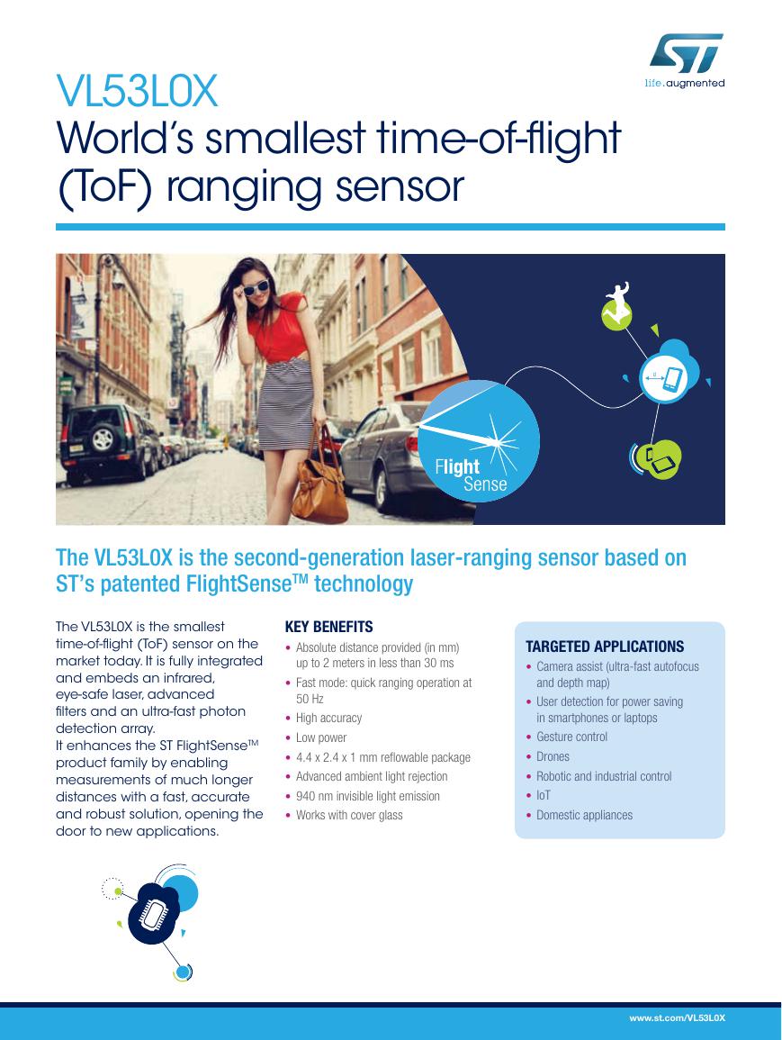 VL53L0X简要说明(En.FLVL53L00216).pdf
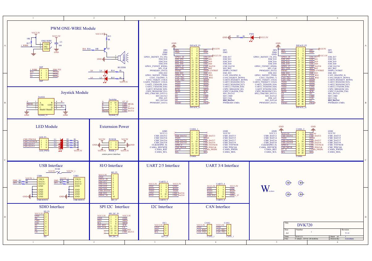 原理图(DVK720-Schematic).pdf
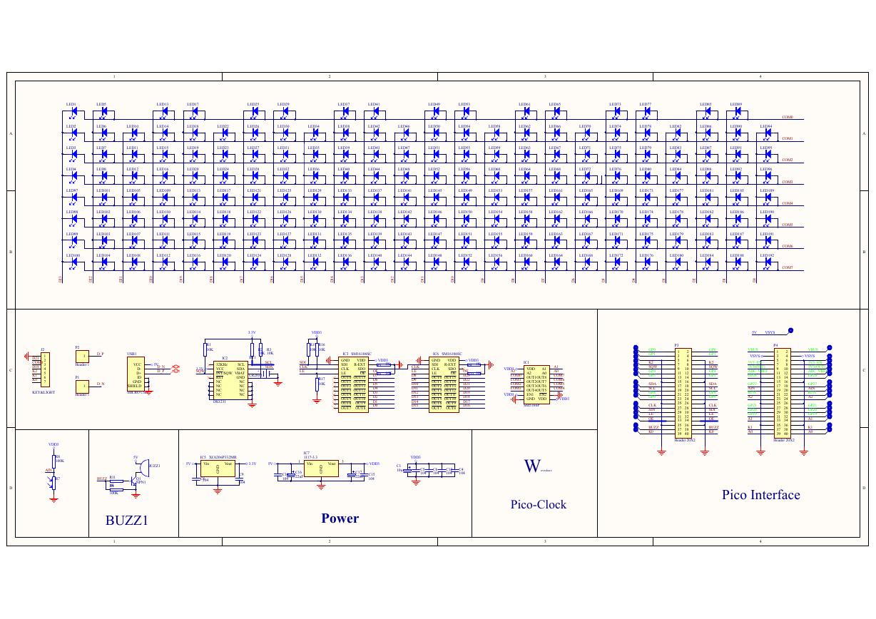 原理图(Pico-Clock-Green-Schdoc).pdf
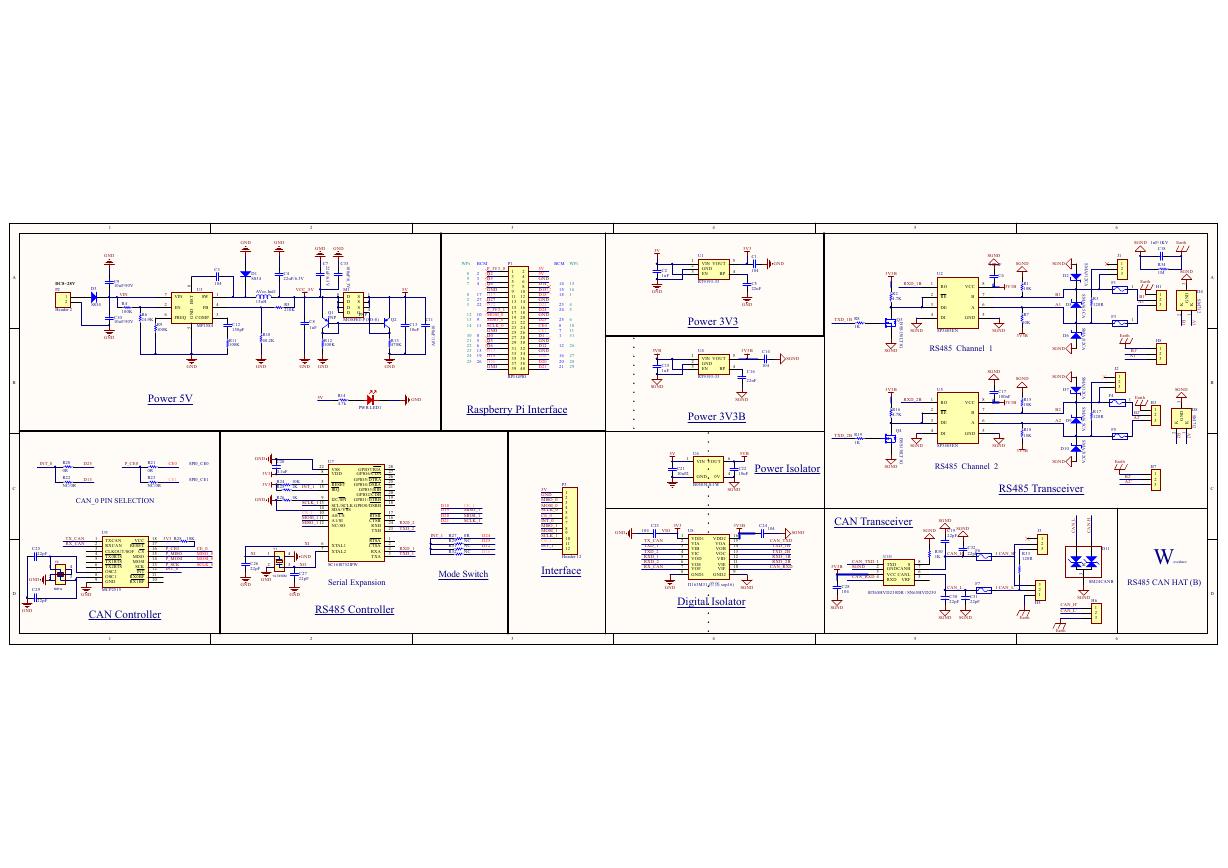 原理图(RS485-CAN-HAT-B-schematic).pdf
 File:SIM7500_SIM7600_SIM7800 Series_SSL_Application Note_V2.00.pdf
 ADS1263(Ads1262).pdf
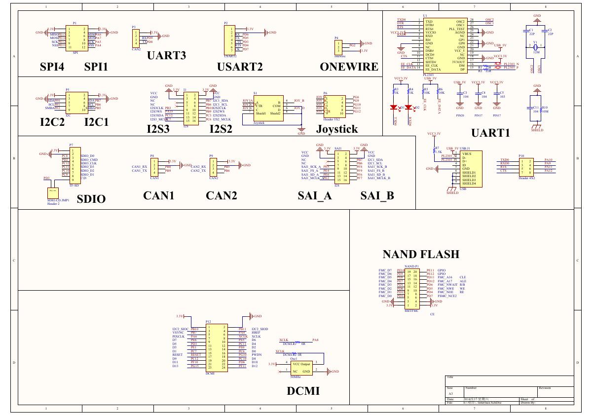 原理图(Open429Z-D-Schematic).pdf
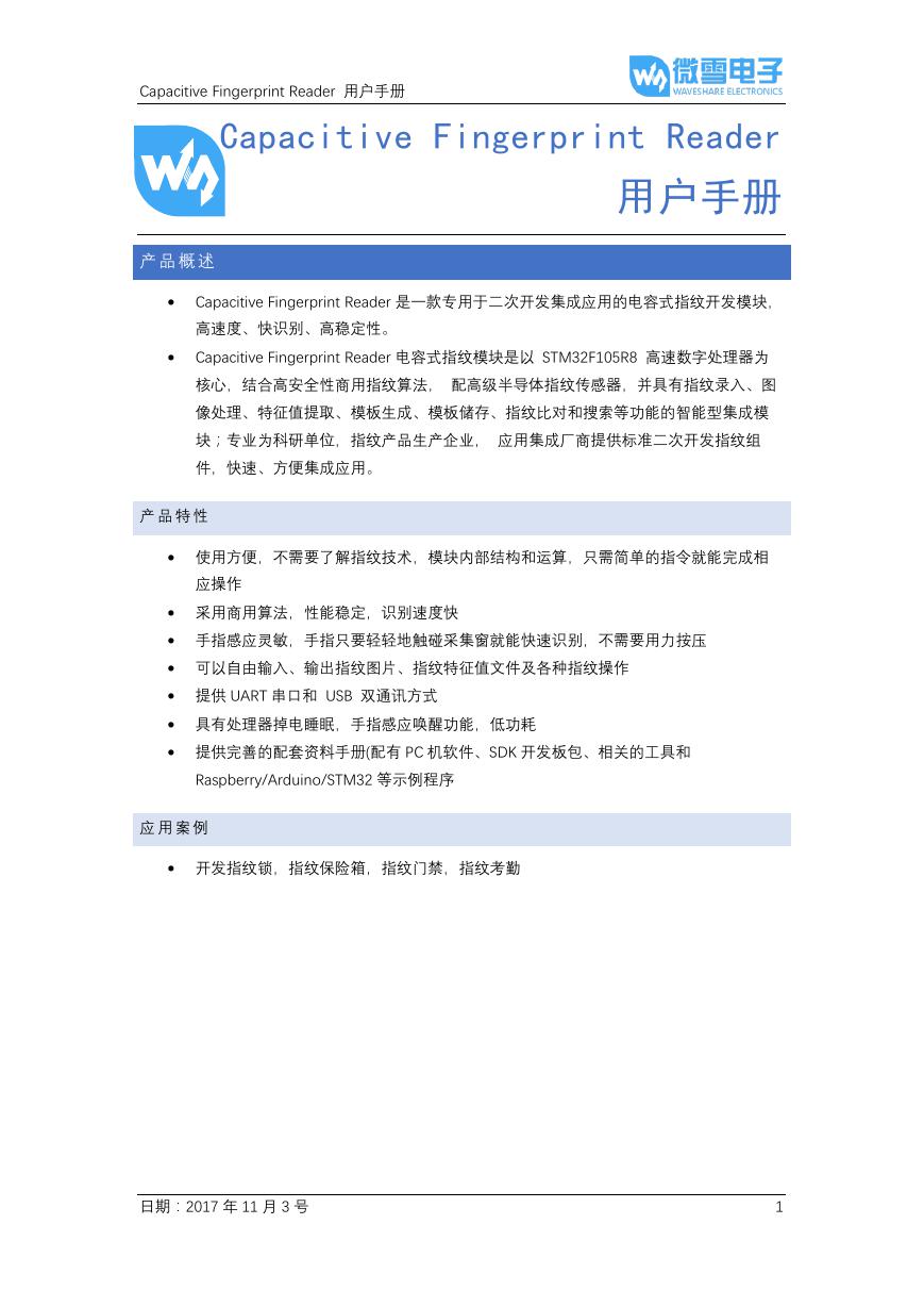 用户手册(Capacitive_Fingerprint_Reader_User_Manual_CN).pdf
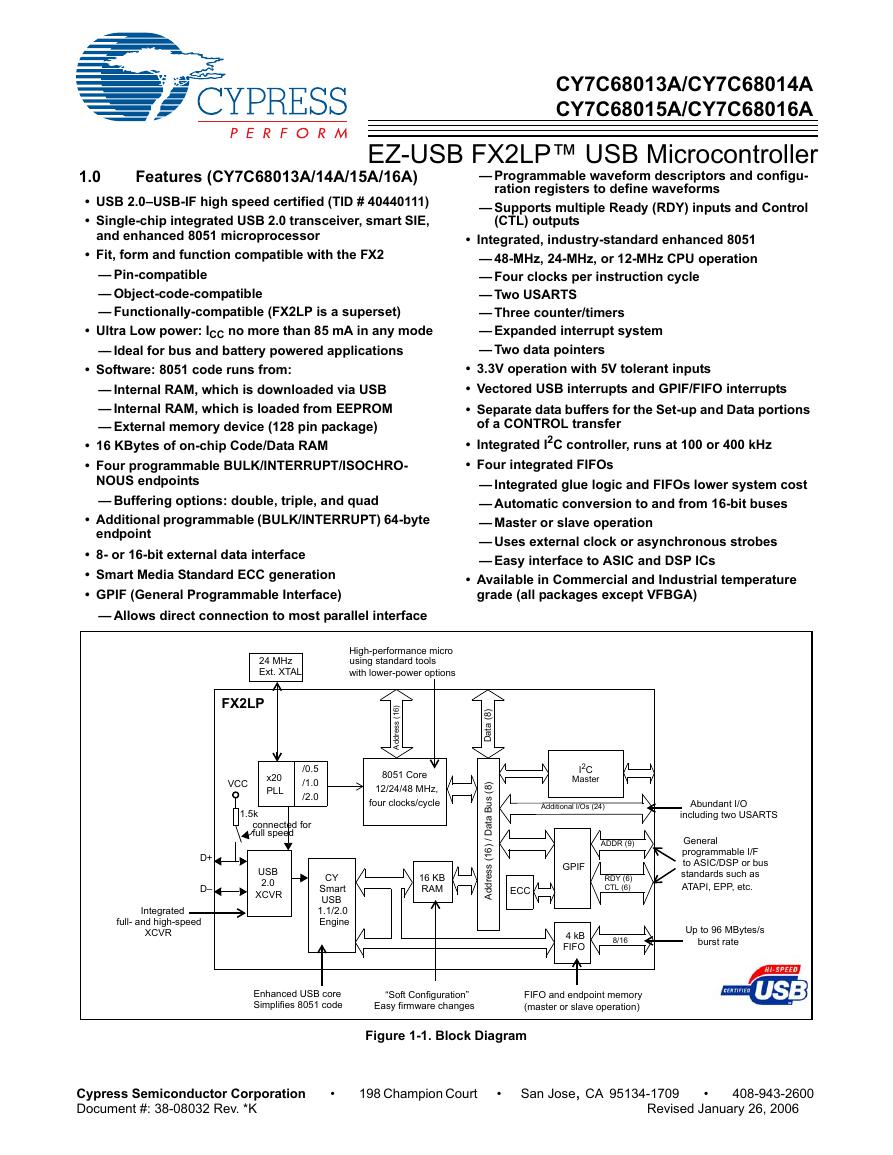 CY7C68013A(英文版)(CY7C68013A).pdf
 TechnicalReference_Dem.pdf