74HC4053; 74HCT4053
Triple 2-channel analog multiplexer/demultiplexer
Rev. 8 — 19 July 2012
Product data sheet
1. General description
The 74HC4053; 74HCT4053 is a high-speed Si-gate CMOS device and is pin compatible
with the HEF4053B. It is specified in compliance with JEDEC standard no. 7A.
The 74HC4053; 74HCT4053 is triple 2-channel analog multiplexer/demultiplexer with a
common enable input (E). Each multiplexer/demultiplexer has two independent
inputs/outputs (nY0 and nY1), a common input/output (nZ) and three digital select
inputs (Sn). With E LOW, one of the two switches is selected (low-impedance ON-state)
by S1 to S3. With E HIGH, all switches are in the high-impedance OFF-state, independent
of S1 to S3.
VCC and GND are the supply voltage pins for the digital control inputs (S0 to S2, and E).
The VCC to GND ranges are 2.0 V to 10.0 V for 74HC4053 and 4.5 V to 5.5 V for
74HCT4053. The analog inputs/outputs (nY0 to nY1, and nZ) can swing between VCC as
a positive limit and VEE as a negative limit. VCC VEE may not exceed 10.0 V.
For operation as a digital multiplexer/demultiplexer, VEE is connected to GND (typically
ground).
2. Features and benefits
Wide analog input voltage range from 5 V to +5 V
Low ON resistance:
80 (typical) at VCC VEE = 4.5 V
70 (typical) at VCC VEE = 6.0 V
60 (typical) at VCC VEE = 9.0 V
Logic level translation: to enable 5 V logic to communicate with 5 V analog signals
Typical ‘break before make’ built-in
ESD protection:
HBM JESD22-A114F exceeds 2000 V
MM JESD22-A115-A exceeds 200 V
CDM JESD22-C101E exceeds 1000 V
Multiple package options
Specified from 40 C to +85 C and 40 C to +125 C
�
NXP Semiconductors
3. Applications
74HC4053; 74HCT4053
Triple 2-channel analog multiplexer/demultiplexer
Analog multiplexing and demultiplexing
Digital multiplexing and demultiplexing
Signal gating
4. Ordering information
Table 1.
Type number
Ordering information
Package
Temperature range Name
40 C to +125 C
DIP16
40 C to +125 C
74HC4053N
74HCT4053N
74HC4053D
74HCT4053D
74HC4053DB
74HCT4053DB
74HC4053PW 40 C to +125 C
74HCT4053PW
74HC4053BQ
74HCT4053BQ
40 C to +125 C
40 C to +125 C
Description
plastic dual in-line package; 16 leads (300 mil)
SO16
SSOP16
plastic small outline package; 16 leads;
body width 3.9 mm
plastic shrink small outline package; 16 leads;
body width 5.3 mm
TSSOP16
plastic thin shrink small outline package; 16 leads;
body width 4.4 mm
DHVQFN16 plastic dual in-line compatible thermal enhanced very
thin quad flat package; no leads; 16 terminals;
body 2.5 3.5 0.85 mm
Version
SOT38-4
SOT109-1
SOT338-1
SOT403-1
SOT763-1
74HC_HCT4053
Product data sheet
All information provided in this document is subject to legal disclaimers.
Rev. 8 — 19 July 2012
© NXP B.V. 2012. All rights reserved.
2 of 32
�
NXP Semiconductors
5. Functional diagram
74HC4053; 74HCT4053
Triple 2-channel analog multiplexer/demultiplexer
E
6
VCC
16
13 1Y1
S1
11
LOGIC
LEVEL
CONVERSION
DECODER
12 1Y0
S2
10
LOGIC
LEVEL
CONVERSION
S3
9
LOGIC
LEVEL
CONVERSION
14 1Z
1 2Y1
2 2Y0
15 2Z
3 3Y1
5 3Y0
4 3Z
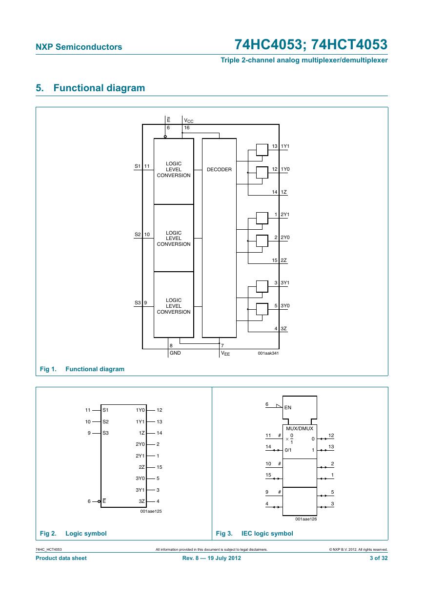
Fig 1.
Functional diagram
8
GND
7
VEE
001aak341
S1
S2
S3
11
10
9
6
E
1Y0
1Y1
1Z
2Y0
2Y1
2Z
3Y0
3Y1
3Z
12
13
14
2
1
15
5
3
4
001aae125
6
11
14
10
15
9
4
#
#
#
EN
MUX/DMUX
0
×
1
0/1
0
1
12
13
2
1
5
3
Fig 2.
Logic symbol
Fig 3.
IEC logic symbol
001aae126
74HC_HCT4053
Product data sheet
All information provided in this document is subject to legal disclaimers.
Rev. 8 — 19 July 2012
© NXP B.V. 2012. All rights reserved.
3 of 32
�
NXP Semiconductors
74HC4053; 74HCT4053
Triple 2-channel analog multiplexer/demultiplexer
from
logic
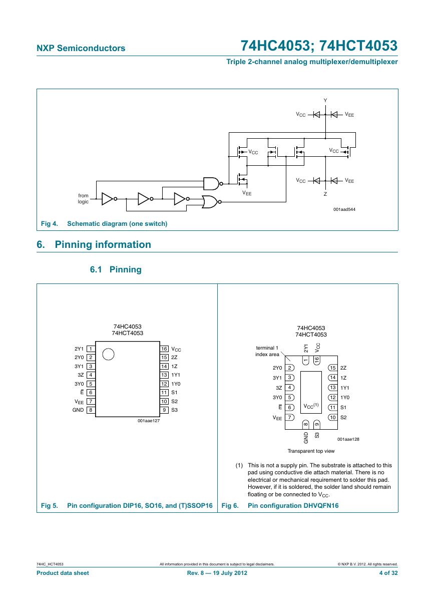
Fig 4.
Schematic diagram (one switch)
6. Pinning information
6.1 Pinning
74HC4053
74HCT4053
2Y1
2Y0
3Y1
3Z
3Y0
E
VEE
GND
1
2
3
4
5
6
7
8
16
15
14
13
12
11
10
9
VCC
2Z
1Z
1Y1
1Y0
S1
S2
S3
001aae127
Y
VCC
VEE
VCC
VCC
VEE
VCC
VEE
Z
001aad544
74HC4053
74HCT4053
1
Y
2
1
C
C
V
6
1
terminal 1
index area
2Y0
3Y1
3Z
3Y0
E
VEE
2
3
4
5
6
7
15
14
13
12
11
10
2Z
1Z
1Y1
1Y0
S1
S2
001aae128
(1)
VCC
8 9
3
S
D
N
G
Transparent top view
Fig 5.
Pin configuration DIP16, SO16, and (T)SSOP16
Fig 6.
(1) This is not a supply pin. The substrate is attached to this
pad using conductive die attach material. There is no
electrical or mechanical requirement to solder this pad.
However, if it is soldered, the solder land should remain
floating or be connected to VCC.
Pin configuration DHVQFN16
74HC_HCT4053
Product data sheet
All information provided in this document is subject to legal disclaimers.
Rev. 8 — 19 July 2012
© NXP B.V. 2012. All rights reserved.
4 of 32
�
NXP Semiconductors
74HC4053; 74HCT4053
Triple 2-channel analog multiplexer/demultiplexer
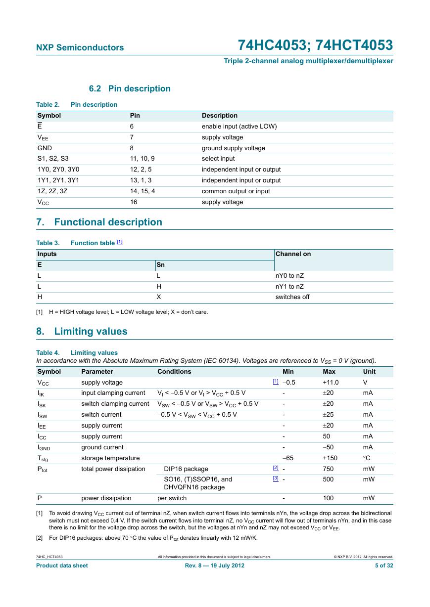
6.2 Pin description
Pin description
Table 2.
Symbol
E
VEE
GND
S1, S2, S3
1Y0, 2Y0, 3Y0
1Y1, 2Y1, 3Y1
1Z, 2Z, 3Z
VCC
Pin
6
7
8
11, 10, 9
12, 2, 5
13, 1, 3
14, 15, 4
16
Description
enable input (active LOW)
supply voltage
ground supply voltage
select input
independent input or output
independent input or output
common output or input
supply voltage
7. Functional description
Function table [1]
Table 3.
Inputs
E
L
L
H
Sn
L
H
X
[1] H = HIGH voltage level; L = LOW voltage level; X = don’t care.
8. Limiting values
Channel on
nY0 to nZ
nY1 to nZ
switches off
Limiting values
Conditions
Min
[1] 0.5
VI < 0.5 V or VI > VCC + 0.5 V
Table 4.
In accordance with the Absolute Maximum Rating System (IEC 60134). Voltages are referenced to VSS = 0 V (ground).
Unit
Symbol
V
VCC
mA
IIK
mA
ISK
mA
ISW
mA
IEE
mA
ICC
mA
IGND
C
Tstg
mW
Ptot
mW
Parameter
supply voltage
input clamping current
switch clamping current VSW < 0.5 V or VSW > VCC + 0.5 V
switch current
supply current
supply current
ground current
storage temperature
total power dissipation
Max
+11.0
20
20
25
20
50
50
+150
750
500
-
-
-
-
-
-
65
-
-
0.5 V < VSW < VCC + 0.5 V
DIP16 package
SO16, (T)SSOP16, and
DHVQFN16 package
[2]
[3]
P
power dissipation
per switch
-
100
mW
[1] To avoid drawing VCC current out of terminal nZ, when switch current flows into terminals nYn, the voltage drop across the bidirectional
switch must not exceed 0.4 V. If the switch current flows into terminal nZ, no VCC current will flow out of terminals nYn, and in this case
there is no limit for the voltage drop across the switch, but the voltages at nYn and nZ may not exceed VCC or VEE.
[2] For DIP16 packages: above 70 C the value of Ptot derates linearly with 12 mW/K.
74HC_HCT4053
Product data sheet
All information provided in this document is subject to legal disclaimers.
Rev. 8 — 19 July 2012
© NXP B.V. 2012. All rights reserved.
5 of 32
�
NXP Semiconductors
74HC4053; 74HCT4053
Triple 2-channel analog multiplexer/demultiplexer
[3] For SO16 packages: above 70 C the value of Ptot derates linearly with 8 mW/K.
For SSOP16 and TSSOP16 packages: above 60 C the value of Ptot derates linearly with 5.5 mW/K.
For DHVQFN16 packages: above 60 C the value of Ptot derates linearly with 4.5 mW/K.
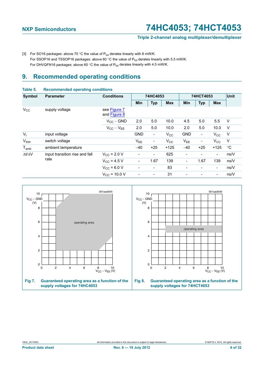
9. Recommended operating conditions
Table 5.
Symbol
Recommended operating conditions
Parameter
Conditions
VCC
supply voltage
VI
VSW
Tamb
t/V
input voltage
switch voltage
ambient temperature
input transition rise and fall
rate
see Figure 7
and Figure 8
VCC GND
VCC VEE
VCC = 2.0 V
VCC = 4.5 V
VCC = 6.0 V
VCC = 10.0 V
10
VCC − GND
(V)
8
6
4
2
0
0
001aad545
operating area
2
4
6
8
10
VCC − VEE (V)
74HC4053
74HCT4053
Unit
Min
Typ
Max
Min
Typ
Max
2.0
2.0
GND
VEE
40
-
-
-
-
5.0
5.0
-
-
+25
-
1.67
-
-
10.0
10.0
VCC
VCC
+125
625
139
83
31
4.5
2.0
GND
VEE
40
-
-
-
-
5.0
5.0
-
-
+25
-
1.67
-
-
5.5
10.0
VCC
VCC
+125
-
139
-
-
V
V
V
V
C
ns/V
ns/V
ns/V
ns/V
10
VCC − GND
(V)
8
6
4
2
0
0
001aad546
operating area
2
4
6
8
10
VCC − VEE (V)
Fig 7. Guaranteed operating area as a function of the
supply voltages for 74HC4053
Fig 8. Guaranteed operating area as a function of the
supply voltages for 74HCT4053
74HC_HCT4053
Product data sheet
All information provided in this document is subject to legal disclaimers.
Rev. 8 — 19 July 2012
© NXP B.V. 2012. All rights reserved.
6 of 32
�
NXP Semiconductors
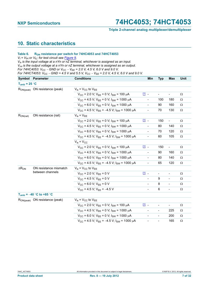
10. Static characteristics
74HC4053; 74HCT4053
Triple 2-channel analog multiplexer/demultiplexer
RON resistance per switch for 74HC4053 and 74HCT4053
Table 6.
VI = VIH or VIL; for test circuit see Figure 9.
Vis is the input voltage at a nYn or nZ terminal, whichever is assigned as an input.
Vos is the output voltage at a nYn or nZ terminal, whichever is assigned as an output.
For 74HC4053: VCC GND or VCC VEE = 2.0 V, 4.5 V, 6.0 V and 9.0 V.
For 74HCT4053: VCC GND = 4.5 V and 5.5 V, VCC VEE = 2.0 V, 4.5 V, 6.0 V and 9.0 V.
Symbol Parameter
Tamb = 25 C
RON(peak) ON resistance (peak)
Conditions
Vis = VCC to VEE
VCC = 2.0 V; VEE = 0 V; ISW = 100 A
VCC = 4.5 V; VEE = 0 V; ISW = 1000 A
VCC = 6.0 V; VEE = 0 V; ISW = 1000 A
VCC = 4.5 V; VEE = 4.5 V; ISW = 1000 A
RON(rail) ON resistance (rail)
Vis = VEE
VCC = 2.0 V; VEE = 0 V; ISW = 100 A
VCC = 4.5 V; VEE = 0 V; ISW = 1000 A
VCC = 6.0 V; VEE = 0 V; ISW = 1000 A
VCC = 4.5 V; VEE = 4.5 V; ISW = 1000 A
Vis = VCC
VCC = 2.0 V; VEE = 0 V; ISW = 100 A
VCC = 4.5 V; VEE = 0 V; ISW = 1000 A
VCC = 6.0 V; VEE = 0 V; ISW = 1000 A
VCC = 4.5 V; VEE = 4.5 V; ISW = 1000 A
Vis = VCC to VEE
VCC = 2.0 V; VEE = 0 V
VCC = 4.5 V; VEE = 0 V
VCC = 6.0 V; VEE = 0 V
VCC = 4.5 V; VEE = 4.5 V
RON
ON resistance mismatch
between channels
Tamb = 40 C to +85 C
RON(peak) ON resistance (peak)
Vis = VCC to VEE
VCC = 2.0 V; VEE = 0 V; ISW = 100 A
VCC = 4.5 V; VEE = 0 V; ISW = 1000 A
VCC = 6.0 V; VEE = 0 V; ISW = 1000 A
VCC = 4.5 V; VEE = 4.5 V; ISW = 1000 A
Min
Typ Max
Unit
[1]
[1]
[1]
[1]
[1]
-
-
-
-
-
-
-
-
-
-
-
-
-
-
-
-
-
-
-
-
-
100
90
70
150
80
70
60
150
90
80
65
-
9
8
6
-
-
-
-
-
180
160
130
-
140
120
105
-
160
140
120
-
-
-
-
-
225
200
165
74HC_HCT4053
Product data sheet
All information provided in this document is subject to legal disclaimers.
Rev. 8 — 19 July 2012
© NXP B.V. 2012. All rights reserved.
7 of 32
�
NXP Semiconductors
74HC4053; 74HCT4053
Triple 2-channel analog multiplexer/demultiplexer
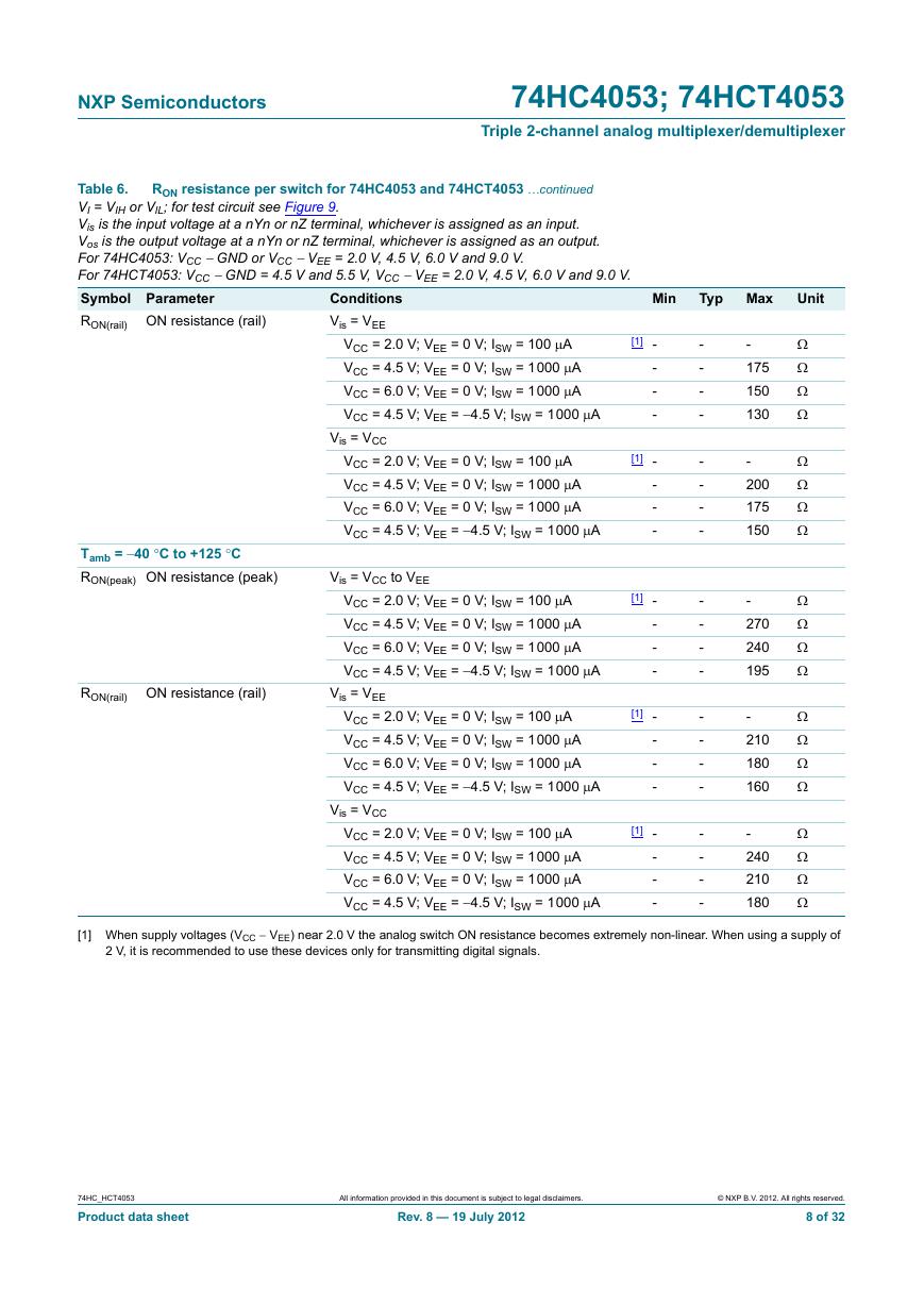
RON resistance per switch for 74HC4053 and 74HCT4053 …continued
Table 6.
VI = VIH or VIL; for test circuit see Figure 9.
Vis is the input voltage at a nYn or nZ terminal, whichever is assigned as an input.
Vos is the output voltage at a nYn or nZ terminal, whichever is assigned as an output.
For 74HC4053: VCC GND or VCC VEE = 2.0 V, 4.5 V, 6.0 V and 9.0 V.
For 74HCT4053: VCC GND = 4.5 V and 5.5 V, VCC VEE = 2.0 V, 4.5 V, 6.0 V and 9.0 V.
Symbol Parameter
RON(rail) ON resistance (rail)
Conditions
Vis = VEE
VCC = 2.0 V; VEE = 0 V; ISW = 100 A
VCC = 4.5 V; VEE = 0 V; ISW = 1000 A
VCC = 6.0 V; VEE = 0 V; ISW = 1000 A
VCC = 4.5 V; VEE = 4.5 V; ISW = 1000 A
Vis = VCC
VCC = 2.0 V; VEE = 0 V; ISW = 100 A
VCC = 4.5 V; VEE = 0 V; ISW = 1000 A
VCC = 6.0 V; VEE = 0 V; ISW = 1000 A
VCC = 4.5 V; VEE = 4.5 V; ISW = 1000 A
Tamb = 40 C to +125 C
RON(peak) ON resistance (peak)
Vis = VCC to VEE
VCC = 2.0 V; VEE = 0 V; ISW = 100 A
VCC = 4.5 V; VEE = 0 V; ISW = 1000 A
VCC = 6.0 V; VEE = 0 V; ISW = 1000 A
VCC = 4.5 V; VEE = 4.5 V; ISW = 1000 A
RON(rail) ON resistance (rail)
Vis = VEE
VCC = 2.0 V; VEE = 0 V; ISW = 100 A
VCC = 4.5 V; VEE = 0 V; ISW = 1000 A
VCC = 6.0 V; VEE = 0 V; ISW = 1000 A
VCC = 4.5 V; VEE = 4.5 V; ISW = 1000 A
Vis = VCC
VCC = 2.0 V; VEE = 0 V; ISW = 100 A
VCC = 4.5 V; VEE = 0 V; ISW = 1000 A
VCC = 6.0 V; VEE = 0 V; ISW = 1000 A
VCC = 4.5 V; VEE = 4.5 V; ISW = 1000 A
Min
Typ Max
Unit
[1]
[1]
[1]
[1]
[1]
-
-
-
-
-
-
-
-
-
-
-
-
-
-
-
-
-
-
-
-
-
-
-
-
-
-
-
-
-
-
-
-
-
-
-
-
-
-
-
-
-
175
150
130
-
200
175
150
-
270
240
195
-
210
180
160
-
240
210
180
[1] When supply voltages (VCC VEE) near 2.0 V the analog switch ON resistance becomes extremely non-linear. When using a supply of
2 V, it is recommended to use these devices only for transmitting digital signals.
74HC_HCT4053
Product data sheet
All information provided in this document is subject to legal disclaimers.
Rev. 8 — 19 July 2012
© NXP B.V. 2012. All rights reserved.
8 of 32
�


 V2版本原理图(Capacitive-Fingerprint-Reader-Schematic_V2).pdf
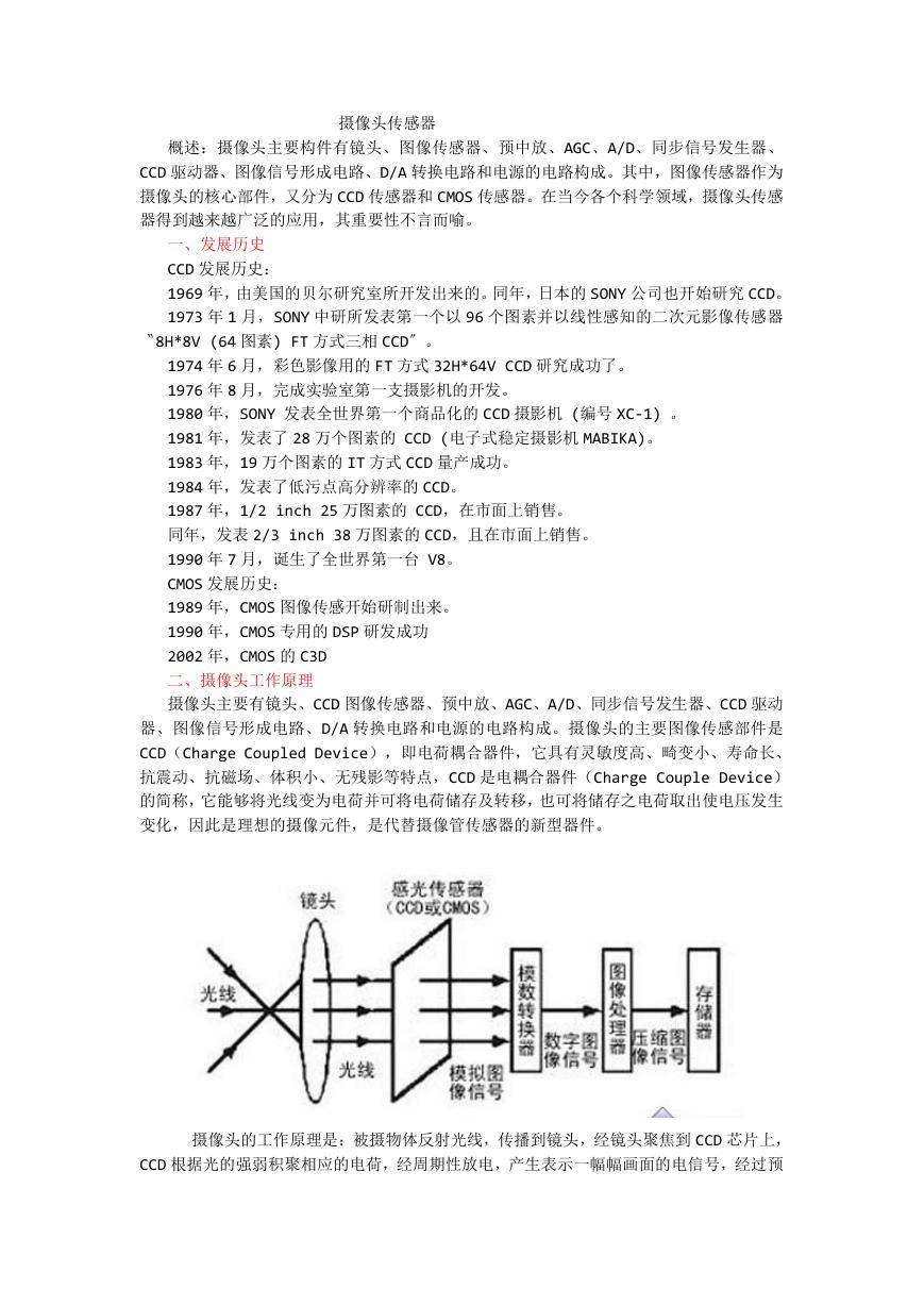 摄像头工作原理.doc
 VL53L0X简要说明(En.FLVL53L00216).pdf
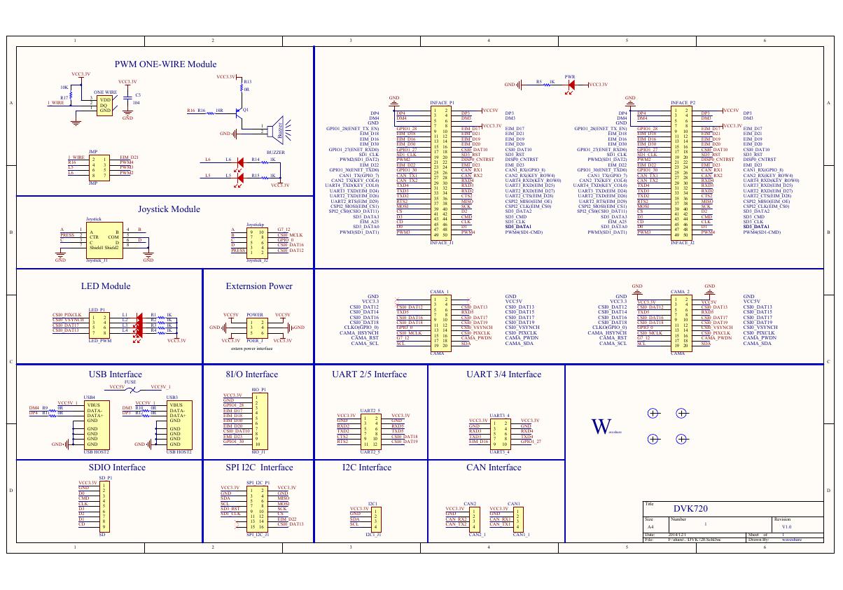 原理图(DVK720-Schematic).pdf
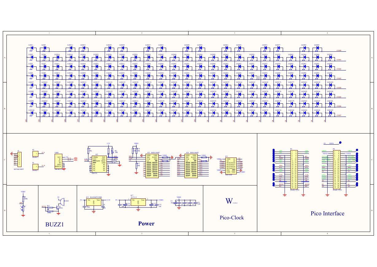 原理图(Pico-Clock-Green-Schdoc).pdf
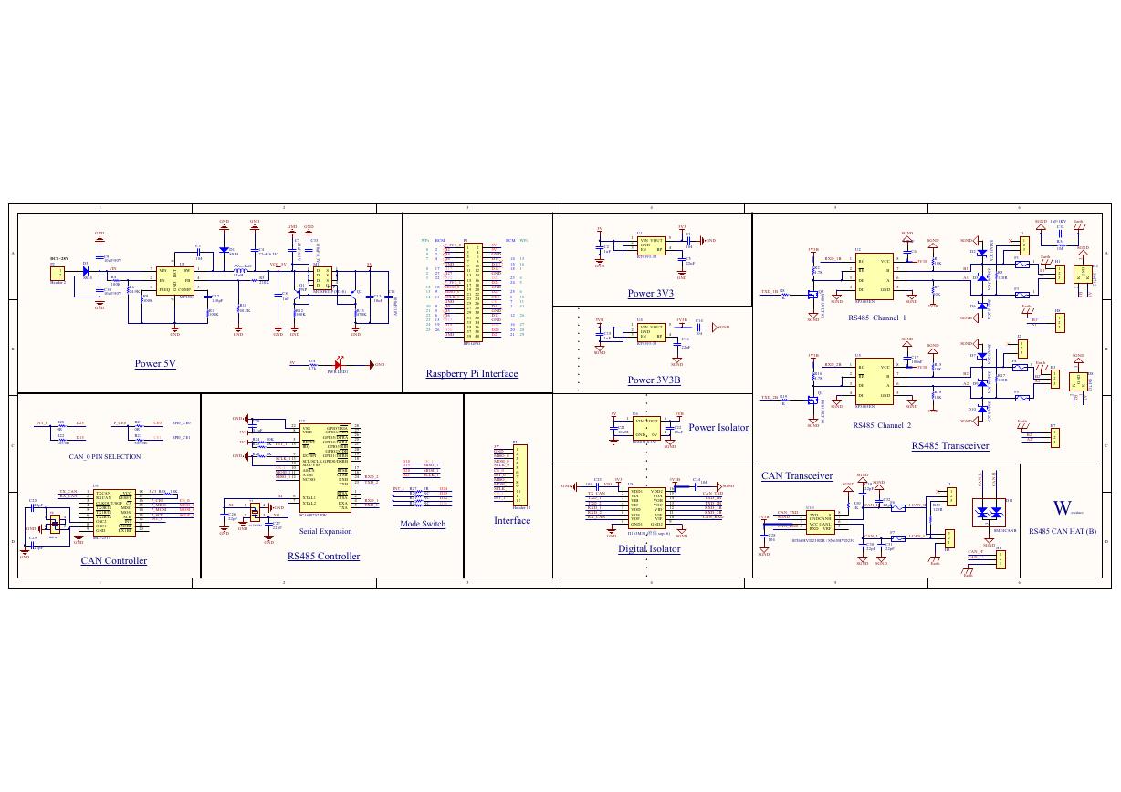 原理图(RS485-CAN-HAT-B-schematic).pdf
 File:SIM7500_SIM7600_SIM7800 Series_SSL_Application Note_V2.00.pdf
 ADS1263(Ads1262).pdf
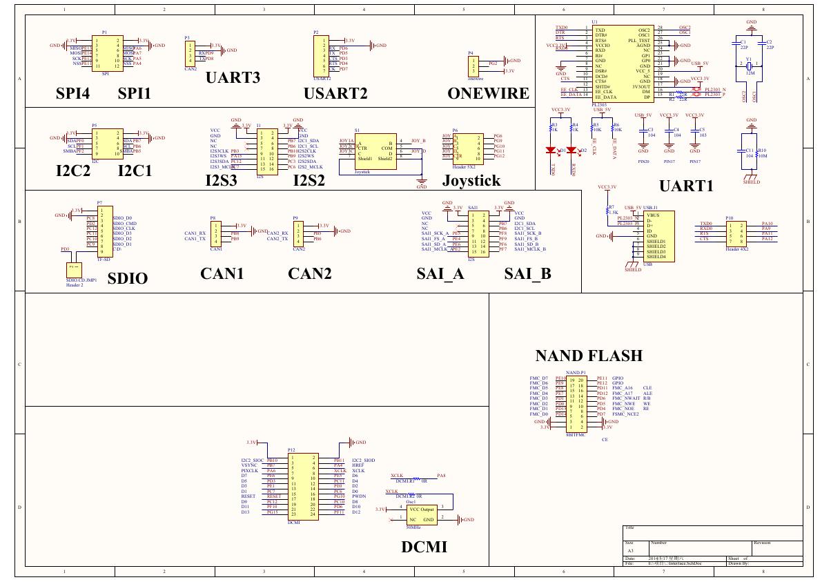 原理图(Open429Z-D-Schematic).pdf
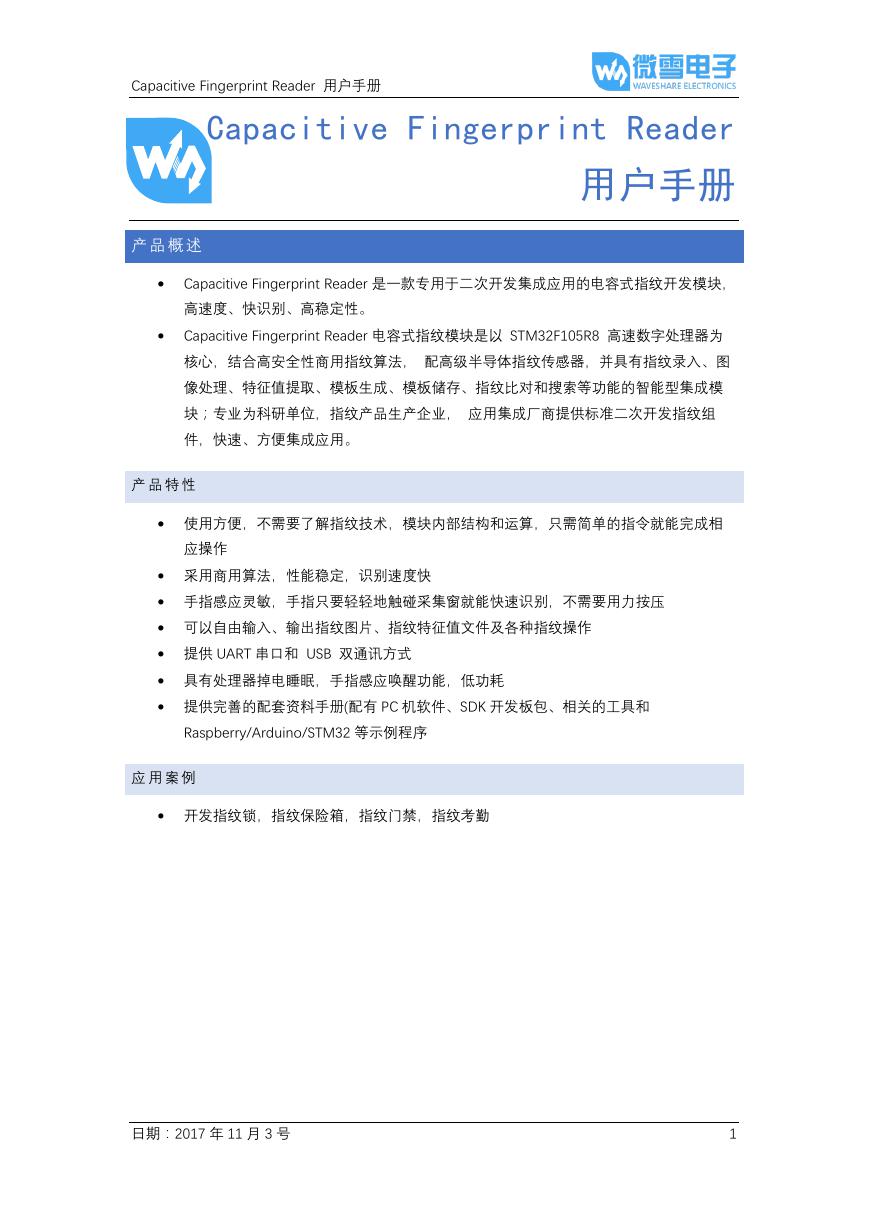 用户手册(Capacitive_Fingerprint_Reader_User_Manual_CN).pdf
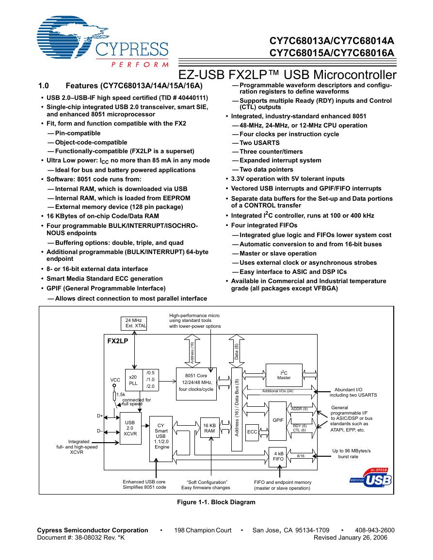 CY7C68013A(英文版)(CY7C68013A).pdf
 TechnicalReference_Dem.pdf