BTA24, BTB24, BTA25, BTA26
and T25 series
25 A Triacs
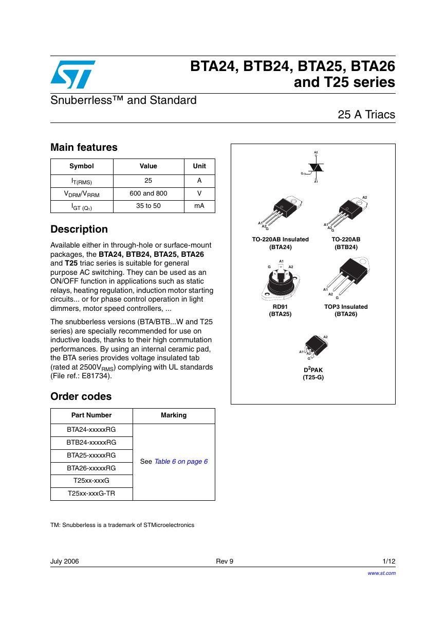
A2
A1
G
A2
A1
A2
G
TO-220AB
(BTB24)
A1
A2
G
TO-220AB Insulated
(BTA24)
A1
G
A2
A1
A2
G
RD91
(BTA25)
TOP3 Insulated
(BTA26)
A2
A1
A2
G
D2PAK
(T25-G)
Snuberrless™ and Standard
Main features
Symbol
IT(RMS)
VDRM/VRRM
IGT (Q1)
Value
25
600 and 800
35 to 50
Unit
A
V
mA
Description
Available either in through-hole or surface-mount
packages, the BTA24, BTB24, BTA25, BTA26
and T25 triac series is suitable for general
purpose AC switching. They can be used as an
ON/OFF function in applications such as static
relays, heating regulation, induction motor starting
circuits... or for phase control operation in light
dimmers, motor speed controllers, ...
The snubberless versions (BTA/BTB...W and T25
series) are specially recommended for use on
inductive loads, thanks to their high commutation
performances. By using an internal ceramic pad,
the BTA series provides voltage insulated tab
(rated at 2500VRMS) complying with UL standards
(File ref.: E81734).
Order codes
Part Number
Marking
BTA24-xxxxxRG
BTB24-xxxxxRG
BTA25-xxxxxRG
BTA26-xxxxxRG
T25xx-xxxG
T25xx-xxxG-TR
See Table 6 on page 6
TM: Snubberless is a trademark of STMicroelectronics
July 2006
Rev 9
1/12
www.st.com
12
�
Characteristics
BTA24, BTB24, BTA25, BTA26 and T25 series
1
Characteristics
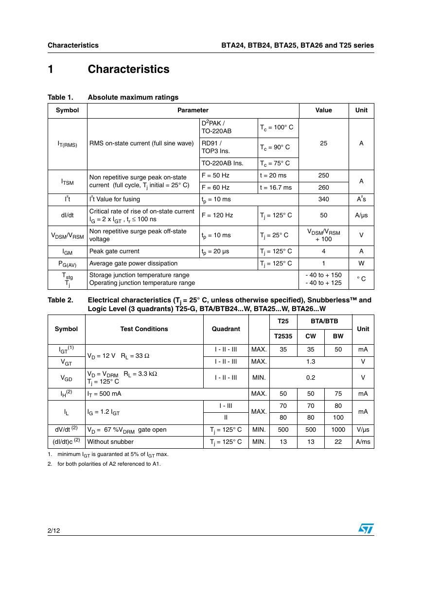
Table 1.
Absolute maximum ratings
Symbol
Parameter
Value
Unit
IT(RMS)
RMS on-state current (full sine wave)
ITSM
I²t
dI/dt
VDSM/VRSM
IGM
PG(AV)
Tstg
Tj
Non repetitive surge peak on-state
current (full cycle, Tj initial = 25° C)
I²t Value for fusing
Critical rate of rise of on-state current
IG = 2 x IGT , tr ≤ 100 ns
Non repetitive surge peak off-state
voltage
Peak gate current
Average gate power dissipation
Storage junction temperature range
Operating junction temperature range
D2PAK /
TO-220AB
RD91 /
TOP3 Ins.
TO-220AB Ins.
F = 50 Hz
F = 60 Hz
tp = 10 ms
Tc = 100° C
Tc = 90° C
Tc = 75° C
t = 20 ms
t = 16.7 ms
F = 120 Hz
Tj = 125° C
tp = 10 ms
tp = 20 µs
Tj = 25° C
Tj = 125° C
Tj = 125° C
25
A
250
260
340
50
VDSM/VRSM
+ 100
4
1
- 40 to + 150
- 40 to + 125
A
A²s
A/µs
V
A
W
° C
Table 2.
Electrical characteristics (Tj = 25° C, unless otherwise specified), Snubberless™ and
Logic Level (3 quadrants) T25-G, BTA/BTB24...W, BTA25...W, BTA26...W
Symbol
Test Conditions
Quadrant
T25
BTA/BTB
T2535
CW
BW
50
75
80
100
1000
22
Unit
mA
V
V
mA
mA
V/µs
A/ms
(1)
IGT
VGT
VGD
(2)
IH
VD = 12 V RL = 33 Ω
VD = VDRM RL = 3.3 kΩ
Tj = 125° C
IT = 500 mA
IL
IG = 1.2 IGT
(2)
dV/dt
(dI/dt)c
VD = 67 %VDRM gate open
(2) Without snubber
I - II - III
I - II - III
MAX.
MAX.
35
I - II - III
MIN.
MAX.
MAX.
I - III
II
Tj = 125° C MIN.
Tj = 125° C MIN.
50
70
80
500
13
35
1.3
0.2
50
70
80
500
13
1. minimum IGT is guaranted at 5% of IGT max.
2.
for both polarities of A2 referenced to A1.
2/12
�
BTA24, BTB24, BTA25, BTA26 and T25 series
Characteristics
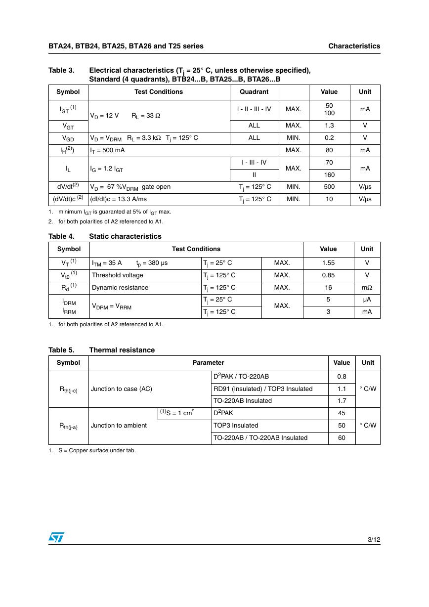
Table 3.
Electrical characteristics (Tj = 25° C, unless otherwise specified),
Standard (4 quadrants), BTB24...B, BTA25...B, BTA26...B
Symbol
Test Conditions
Quadrant
Value
(1)
IGT
VGT
VGD
(2))
IH
VD = 12 V RL = 33 Ω
VD = VDRM RL = 3.3 kΩ Tj = 125° C
IT = 500 mA
IL
IG = 1.2 IGT
dV/dt(2)
(dV/dt)c
(2)
VD = 67 %VDRM gate open
(dI/dt)c = 13.3 A/ms
1. minimum IGT is guaranted at 5% of IGT max.
2.
for both polarities of A2 referenced to A1.
Table 4.
Static characteristics
I - II - III - IV
MAX.
ALL
ALL
I - III - IV
II
Tj = 125° C
Tj = 125° C
MAX.
MIN.
MAX.
MAX.
MIN.
MIN.
50
100
1.3
0.2
80
70
160
500
10
Unit
mA
V
V
mA
mA
V/µs
V/µs
Symbol
Test Conditions
Value
Unit
(1)
VT
Vt0
Rd
(1)
(1)
ITM = 35 A tp = 380 µs
Threshold voltage
Dynamic resistance
IDRM
IRRM
VDRM = VRRM
1.
for both polarities of A2 referenced to A1.
Table 5.
Thermal resistance
Tj = 25° C
Tj = 125° C
Tj = 125° C
Tj = 25° C
Tj = 125° C
MAX.
MAX.
MAX.
MAX.
1.55
0.85
16
5
3
V
V
mΩ
µA
mA
Symbol
Parameter
Value
Unit
Rth(j-c)
Junction to case (AC)
RD91 (Insulated) / TOP3 Insulated
D2PAK / TO-220AB
Rth(j-a)
Junction to ambient
1. S = Copper surface under tab.
(1)S = 1 cm²
TO-220AB Insulated
D2PAK
TOP3 Insulated
TO-220AB / TO-220AB Insulated
0.8
1.1
1.7
45
50
60
° C/W
° C/W
3/12
�
Characteristics
BTA24, BTB24, BTA25, BTA26 and T25 series
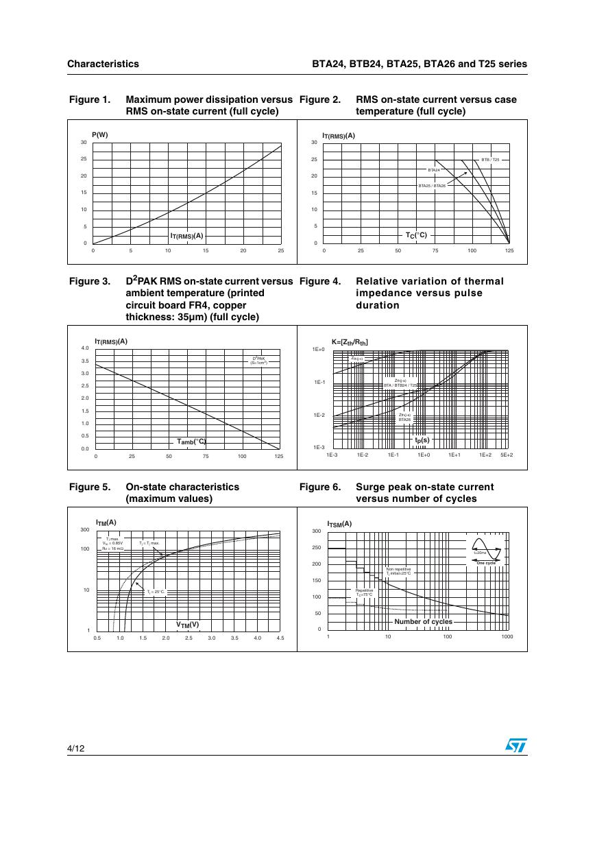
Figure 1. Maximum power dissipation versus
Figure 2.
RMS on-state current (full cycle)
RMS on-state current versus case
temperature (full cycle)
P(W)
30
25
20
15
10
5
0
I
T(RMS)
(A)
I
T(RMS)
(A)
30
25
20
15
10
5
0
BTB / T25
BTA24
BTA25 / BTA26
T (°C)
C
0
5
10
15
20
25
0
25
50
75
100
125
Figure 3.
D2PAK RMS on-state current versus
ambient temperature (printed
circuit board FR4, copper
thickness: 35µm) (full cycle)
Figure 4.
Relative variation of thermal
impedance versus pulse
duration
I
T(RMS)
(A)
4.0
3.5
3.0
2.5
2.0
1.5
1.0
0.5
0.0
K=[Z /Rth th]
1E+0
Zth(j-c)
2
D PAK
2
(S=1cm )
1E-1
1E-2
1E-3
Z
th(j-a)
BTA / BTB24 / T25
Z
th(j-a)
BTA26
t (s)p
T
amb
(°C)
0
25
50
75
100
125
1E-3
1E-2
1E-1
1E+0
1E+1
1E+2
5E+2
Figure 5. On-state characteristics
Figure 6.
(maximum values)
Surge peak on-state current
versus number of cycles
I
TM
(A)
j
T max.
to
d
V = 0.85V
Ω
R = 16 m
300
100
10
1
T =j T max.
j
T = 25°C
.
j
V (V)
TM
I
TSM
(A)
300
250
200
150
100
50
0
t=20ms
One cycle
Non repetitive
T initial=25°C
j
Repetitive
T =75°C
C
Number of cycles
0.5
1.0
1.5
2.0
2.5
3.0
3.5
4.0
4.5
1
10
100
1000
4/12
�
BTA24, BTB24, BTA25, BTA26 and T25 series
Characteristics
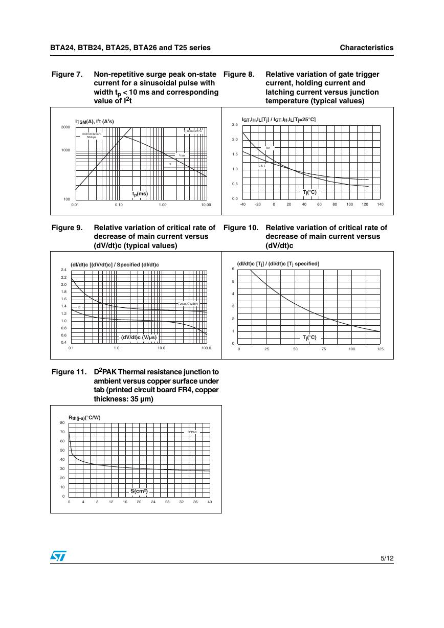
Figure 7.
Non-repetitive surge peak on-state
current for a sinusoidal pulse with
width tp < 10 ms and corresponding
value of I2t
Figure 8.
Relative variation of gate trigger
current, holding current and
latching current versus junction
temperature (typical values)
I
3000
1000
TSM
2
(A), I t (A s)
2
dI/dt limitation:
50A/µs
T initial=25°C
j
ITSM
I t2
t (ms)
p
I
GT H L j
,I [T ] /
,I
I
GT H L j
,I [T =25°C]
,I
IGT
IH & IL
T (°C)
j
2.5
2.0
1.5
1.0
0.5
0.0
100
0.01
Figure 9.
0.10
1.00
10.00
-40
-20
0
20
40
60
80
100
120
140
Relative variation of critical rate of
decrease of main current versus
(dV/dt)c (typical values)
Figure 10. Relative variation of critical rate of
decrease of main current versus
(dV/dt)c
(dI/dt)c [T ] /
j
(dI/dt)c [T sj
pecified]
T (°C)
j
0
25
50
75
100
125
(dI/dt)c [(dV/dt)c] / Specified (dI/dt)c
2.4
2.2
2.0
1.8
1.6
1.4
1.2
1.0
0.8
0.6
0.4
B
T2535/CW/BW
(dV/dt)c (V/µs)
0.1
1.0
10.0
100.0
6
5
4
3
2
1
0
Figure 11. D2PAK Thermal resistance junction to
ambient versus copper surface under
tab (printed circuit board FR4, copper
thickness: 35 µm)
80
70
60
50
40
30
20
10
0
R
th(j-a)
(°C/W)
D PAK2
S(cm²)
0
4
8
12
16
20
24
28
32
36
40
5/12
�
Ordering information scheme
BTA24, BTB24, BTA25, BTA26 and T25 series
2
Ordering information scheme
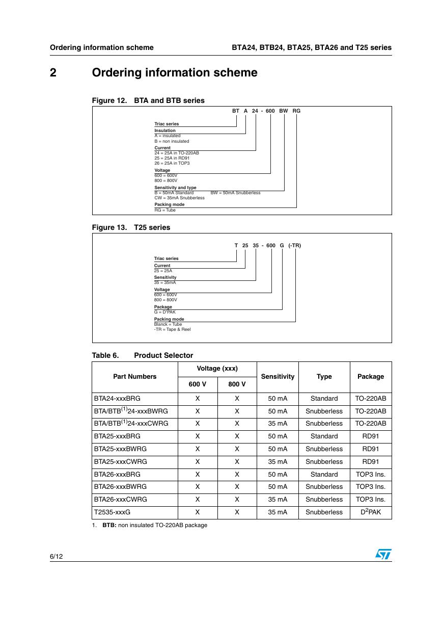
Figure 12. BTA and BTB series
BT A 24 - 600 BW RG
Triac series
Insulation
A = insulated
B = non insulated
Current
24 = 25A in TO-220AB
25 = 25A in RD91
26 = 25A in TOP3
Voltage
600 = 600V
800 = 800V
Sensitivity and type
B = 50mA Standard
CW = 35mA
Packing mode
RG = Tube
Snubberless
BW = 50mA Snubberless
Figure 13. T25 series
T 25 35 - 600 G (-TR)
Triac series
Current
25 = 25A
Sensitivity
35 = 35mA
Voltage
600 = 600V
800 = 800V
Package
G = D PAK
Packing mode
Blanck = Tube
-TR = Tape & Reel
2
Table 6.
Product Selector
Part Numbers
BTA24-xxxBRG
BTA/BTB(1)24-xxxBWRG
BTA/BTB(1)24-xxxCWRG
BTA25-xxxBRG
BTA25-xxxBWRG
BTA25-xxxCWRG
BTA26-xxxBRG
BTA26-xxxBWRG
BTA26-xxxCWRG
T2535-xxxG
Voltage (xxx)
600 V
800 V
Sensitivity
Type
Package
X
X
X
X
X
X
X
X
X
X
X
X
X
X
X
X
X
X
X
X
50 mA
50 mA
35 mA
50 mA
50 mA
35 mA
50 mA
50 mA
35 mA
35 mA
Standard
TO-220AB
Snubberless
TO-220AB
Snubberless
TO-220AB
Standard
Snubberless
Snubberless
RD91
RD91
RD91
Standard
TOP3 Ins.
Snubberless
TOP3 Ins.
Snubberless
TOP3 Ins.
Snubberless
D2PAK
1. BTB: non insulated TO-220AB package
6/12
�
BTA24, BTB24, BTA25, BTA26 and T25 series
Package information
3
Package information
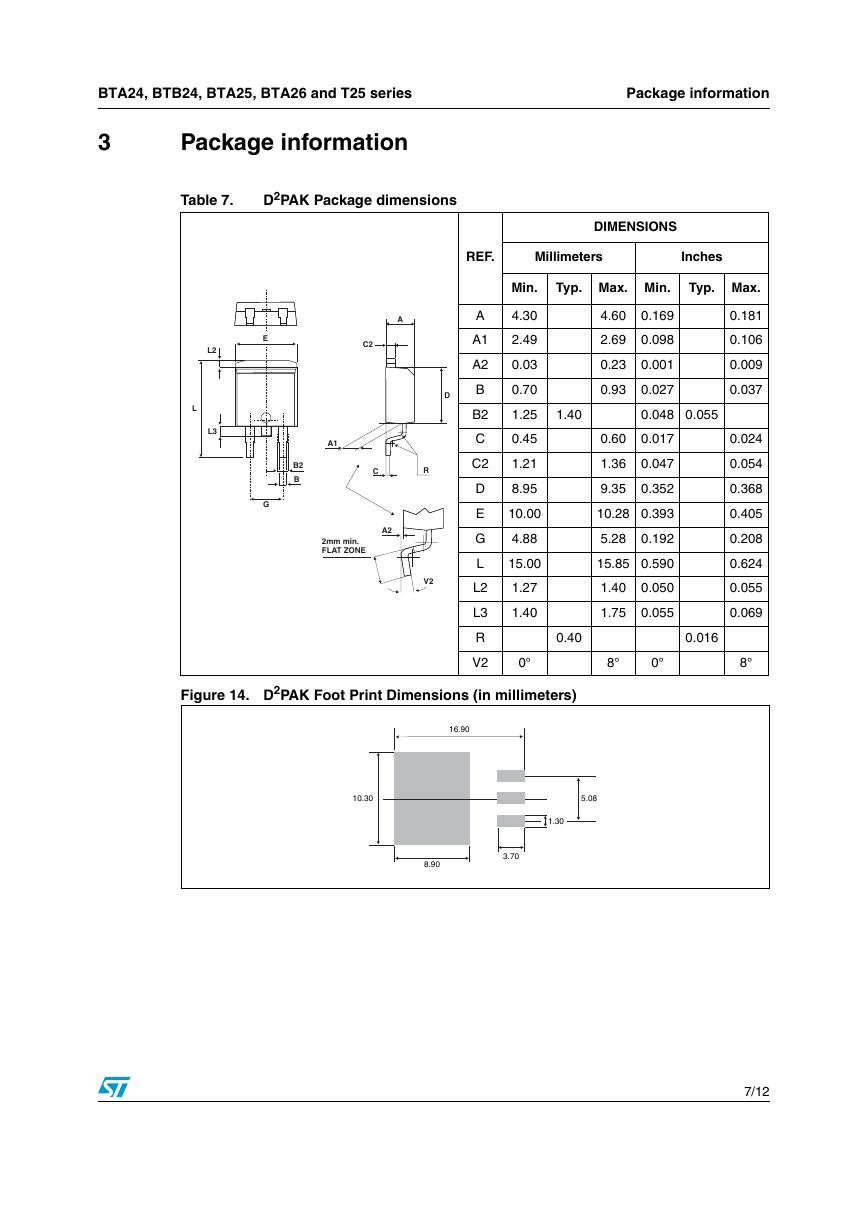
Table 7.
D2PAK Package dimensions
L2
L
L3
E
G
A
C2
D
A1
B2
B
C
R
A2
2mm min.
FLAT ZONE
V2
DIMENSIONS
REF.
Millimeters
Inches
Min.
Typ. Max. Min.
Typ. Max.
A
A1
A2
B
B2
C
C2
D
E
G
L
L2
L3
R
V2
4.30
2.49
0.03
0.70
1.25
0.45
1.21
8.95
10.00
4.88
15.00
1.27
1.40
4.60
0.169
2.69
0.098
0.23
0.001
0.93
0.027
1.40
0.048 0.055
0.60
0.017
1.36
0.047
9.35
0.352
10.28 0.393
5.28
0.192
15.85 0.590
1.40
0.050
1.75
0.055
0.181
0.106
0.009
0.037
0.024
0.054
0.368
0.405
0.208
0.624
0.055
0.069
0.40
0.016
0°
8°
0°
8°
Figure 14. D2PAK Foot Print Dimensions (in millimeters)
16.90
10.30
5.08
1.30
8.90
3.70
7/12
�
Package information
BTA24, BTB24, BTA25, BTA26 and T25 series
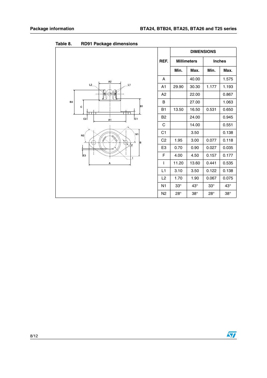
Table 8.
RD91 Package dimensions
L2
A2
L1
B2
C
C2
N2
E3
B1
A1
C1
N1
B
F
I
A
DIMENSIONS
REF.
Millimeters
Inches
Min.
Max.
Min.
Max.
A
A1
A2
B
B1
B2
C
C1
C2
E3
F
I
L1
L2
N1
N2
40.00
30.30
22.00
27.00
16.50
24.00
14.00
3.50
3.00
0.90
4.50
29.90
13.50
1.95
0.70
4.00
1.177
0.531
1.575
1.193
0.867
1.063
0.650
0.945
0.551
0.138
0.077
0.118
0.027
0.157
0.035
0.177
11.20
13.60
0.441
0.535
3.10
1.70
33°
28°
3.50
1.90
43°
38°
0.122
0.067
0.138
0.075
33°
28°
43°
38°
8/12
�


 V2版本原理图(Capacitive-Fingerprint-Reader-Schematic_V2).pdf
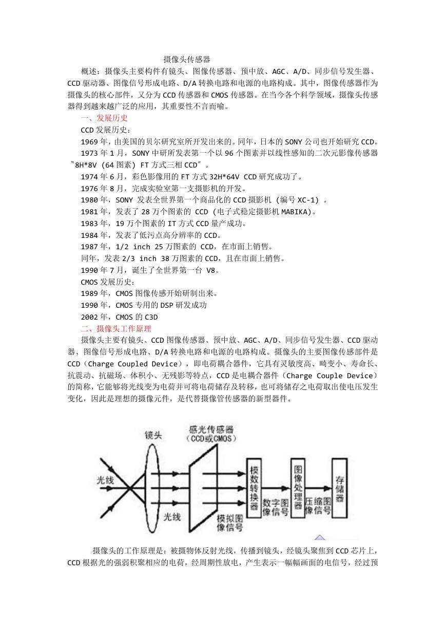 摄像头工作原理.doc
 VL53L0X简要说明(En.FLVL53L00216).pdf
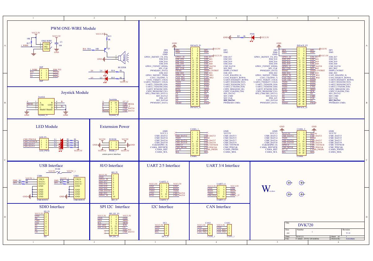 原理图(DVK720-Schematic).pdf
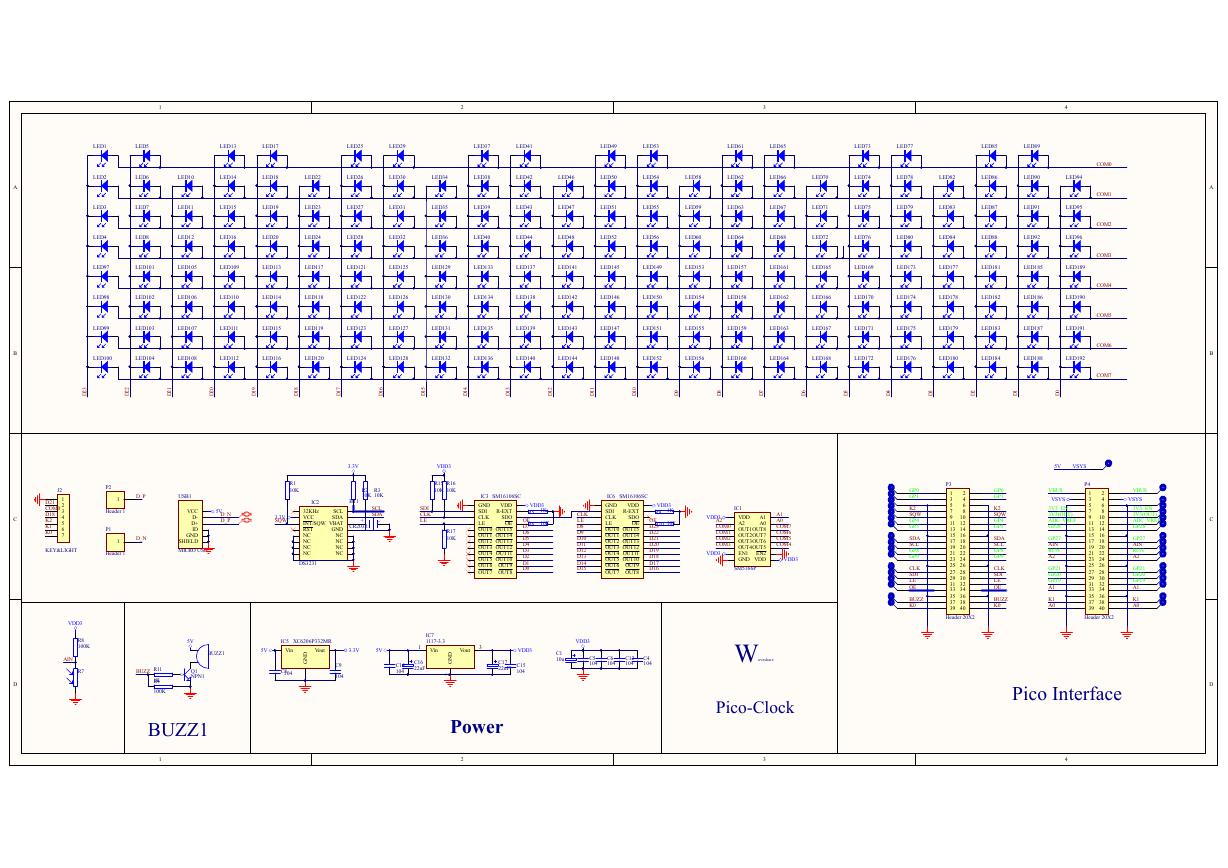 原理图(Pico-Clock-Green-Schdoc).pdf
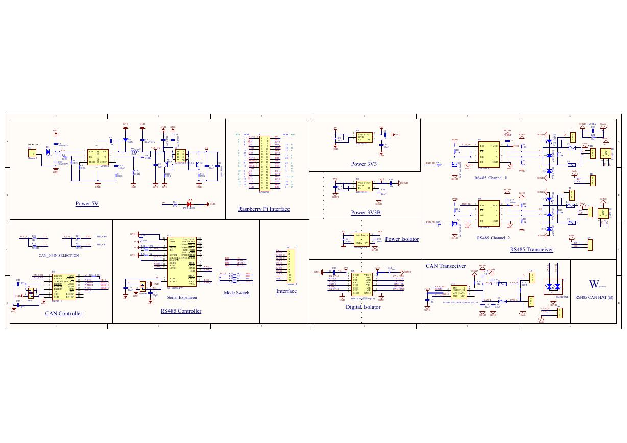 原理图(RS485-CAN-HAT-B-schematic).pdf
 File:SIM7500_SIM7600_SIM7800 Series_SSL_Application Note_V2.00.pdf
 ADS1263(Ads1262).pdf
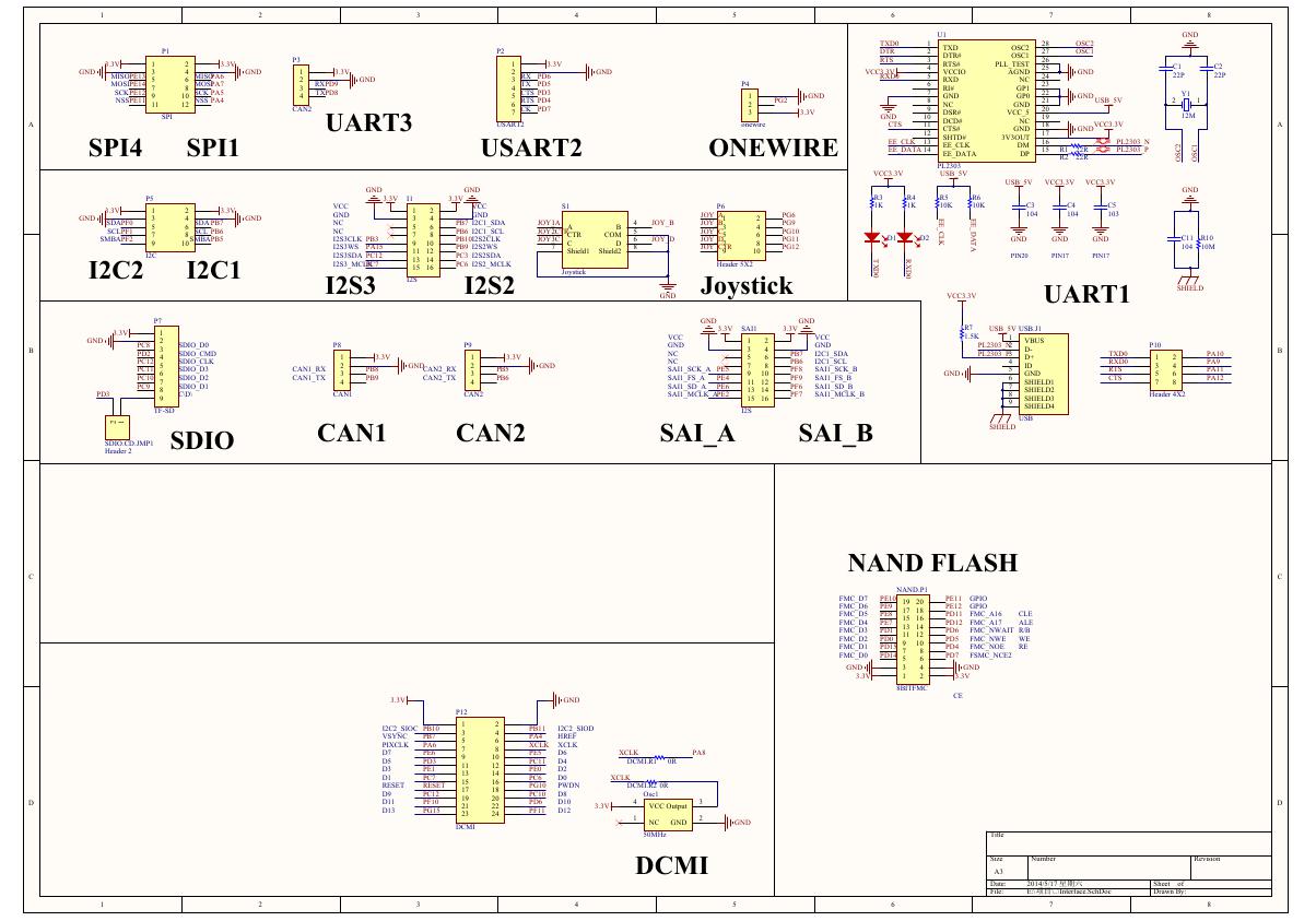 原理图(Open429Z-D-Schematic).pdf
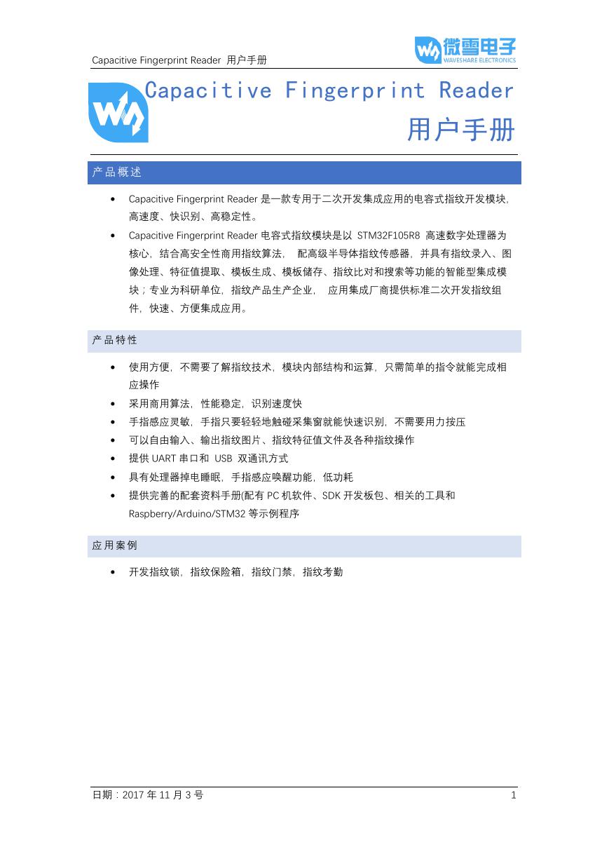 用户手册(Capacitive_Fingerprint_Reader_User_Manual_CN).pdf
 CY7C68013A(英文版)(CY7C68013A).pdf
 TechnicalReference_Dem.pdf