PRODUCT SPECIFICATIONS
For Customer:
Customer Model No.
ModuleNo.:
10.1F
1. Table of Contents
□ : APPROVAL FOR SPECIFICATION
□ : APPROVAL FOR SAMPLE
Date:2021.12.10
Version :A
No.
Item
Page
1
2
3
4
5
6
7
8
9
Cover Sheet(Table of Contents)
Revision Record
General Specifications
Outline Drawing
Absolute Maximum Ratings
Electrical Specifications and Timing Characteristics
Optical Characteristics
Reliability Test Items and Criteria
Quality Level
10
Packing Reliability
ForFor Customer
Customer’’ss Acceptance:
Acceptance:
Approved By
Comment
PREPARED
CHECKED
VERIFIED BY QA
VERIFIED BY R&D
DEPT
DEPT
�
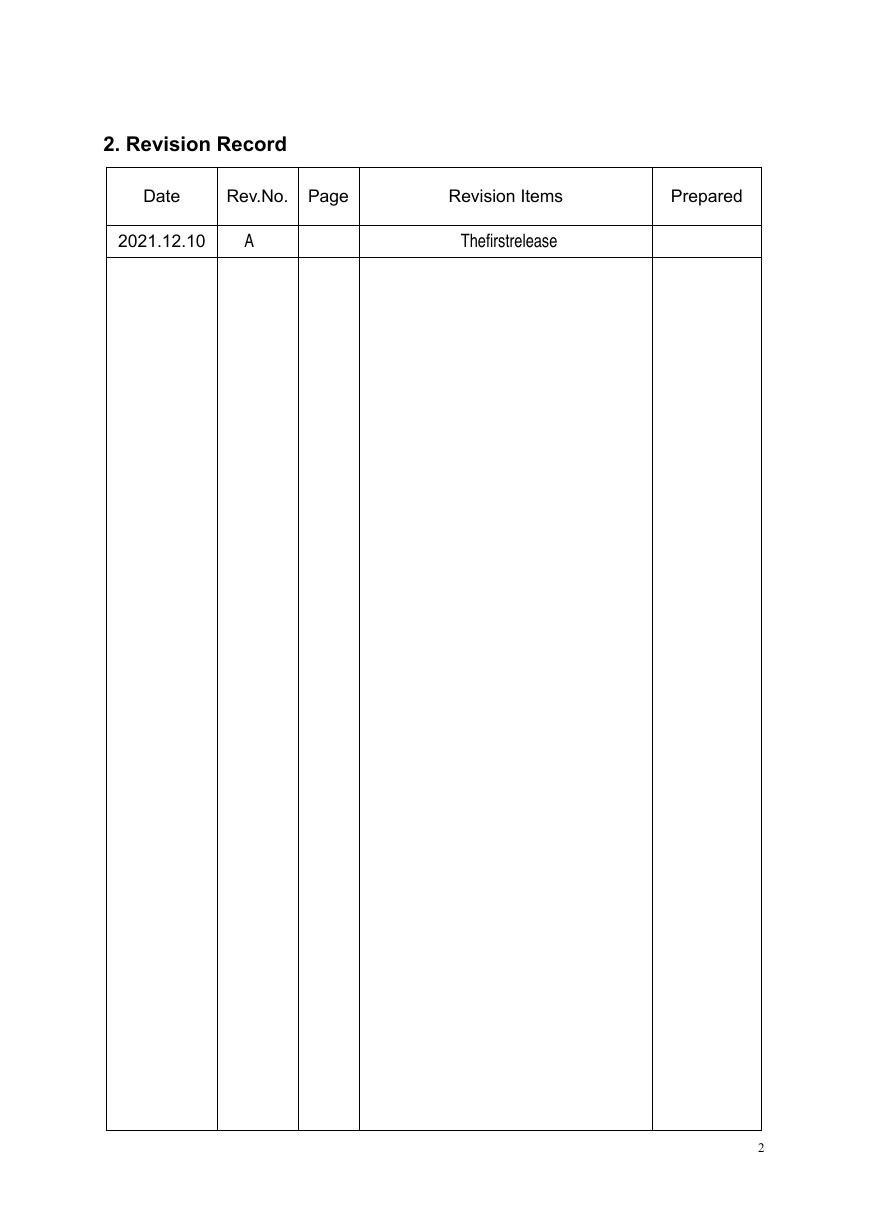
2. Revision Record
Date
Rev.No. Page
Revision Items
Prepared
2021.12.10
A
Thefirstrelease
2
�
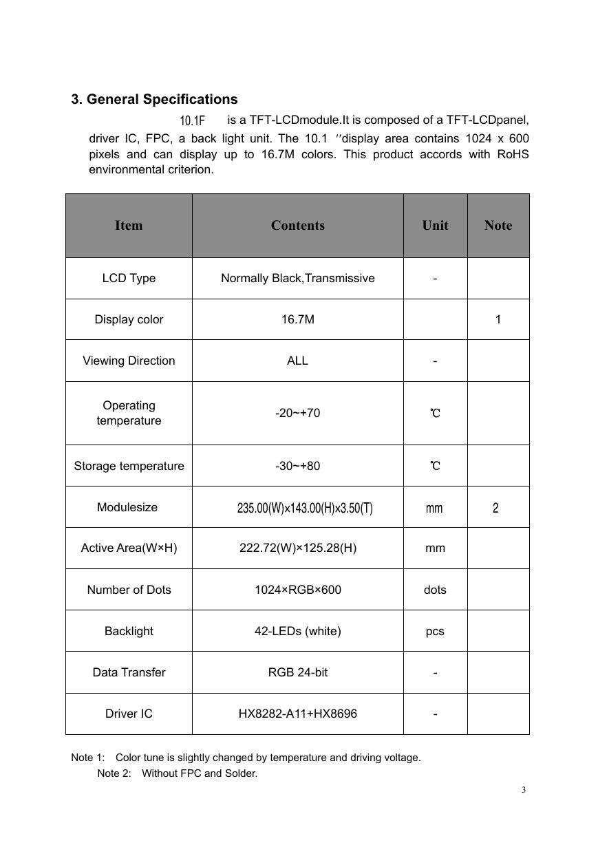
3. General Specifications
10.1F
is a TFT-LCDmodule.It is composed of a TFT-LCDpanel,
driver IC, FPC, a back light unit. The 10.1 ′′display area contains 1024 x 600
pixels and can display up to 16.7M colors. This product accords with RoHS
environmental criterion.
Item
Contents
Unit
Note
1
2
LCD Type
Normally Black,Transmissive
Display color
Viewing Direction
Operating
temperature
16.7M
ALL
-20~+70
Storage temperature
-30~+80
Modulesize
235.00(W)×143.00(H)×3.50(T)
Active Area(W×H)
222.72(W)×125.28(H)
Number of Dots
1024×RGB×600
Backlight
42-LEDs (white)
Data Transfer
RGB 24-bit
Driver IC
HX8282-A11+HX8696
-
-
℃
℃
mm
mm
dots
pcs
-
-
Note 1: Color tune is slightly changed by temperature and driving voltage.
Note 2: Without FPC and Solder.
3
�
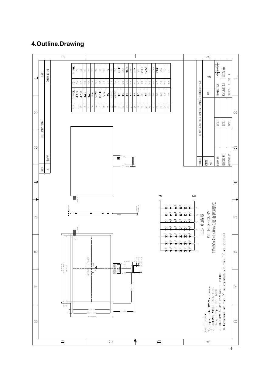
4.Outline.Drawing
E
T
A
D
N
O
I
T
P
I
R
C
S
E
D
版
初
V
E
R
A
K
A
5.00±0.3
A
K
5
0
.
0
±
3
.
0
)
C
P
F
+
强
补
I
P
(
图
路
电
D
E
L
V
4
.
0
2
-
8
.
6
1
f
V
)
试
测
流
电
定
(
A
m
0
4
1
=
7
*
0
2
=
F
I
3.50±0.30
3
0
.
0
±
5
3
.
0
3
0
.
0
±
0
5
.
0
5
0
.
0
±
0
5
.
4
2
0
1
.
0
±
0
5
.
5
2
0
5
.
0
±
0
6
.
3
0
1
55.00±0.50
0
2
.
0
±
0
5
.
3
纸
拉
易
纸
拉
易
0
2
.
0
±
0
0
.
5
3
2
)
Z
B
(
0
2
.
0
±
2
7
.
5
2
2
)
A
.
A
(
2
7
.
2
2
2
9
8
.
3
9
3
.
5
8.47
125.28(A.A)
7.01
128.19±0.20(BZ)
*143.00±0.20
1
F
O
1
:
T
E
E
H
S
4
�
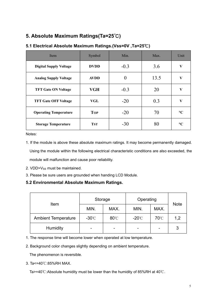
5. Absolute Maximum Ratings(Ta=25℃)
5.1 Electrical Absolute Maximum Ratings.(Vss=0V ,Ta=25℃)
Item
Digital Supply Voltage
Analog Supply Voltage
TFT Gate ON Voltage
TFT Gate OFF Voltage
Operating Temperature
Storage Temperature
Notes:
Symbol
DVDD
AVDD
VGH
VGL
TOP
TST
Min.
-0.3
0
-0.3
-20
-20
-30
Max.
3.6
13.5
20
0.3
70
80
Unit
V
V
V
V
°C
°C
1. If the module is above these absolute maximum ratings. It may become permanently damaged.
Using the module within the following electrical characteristic conditions are also exceeded, the
module will malfunction and cause poor reliability.
2. VDD>VSS must be maintained.
3. Please be sure users are grounded when handing LCD Module.
5.2 Environmental Absolute Maximum Ratings.
Item
Ambient Temperature
Humidity
Storage
Operating
MIN.
-30℃
-
MAX.
80℃
-
MIN.
-20℃
-
MAX.
70℃
-
Note
1,2
3
1. The response time will become lower when operated at low temperature.
2. Background color changes slightly depending on ambient temperature.
The phenomenon is reversible.
3. Ta<=40℃:85%RH MAX.
Ta>=40℃:Absolute humidity must be lower than the humidity of 85%RH at 40℃.
5
�
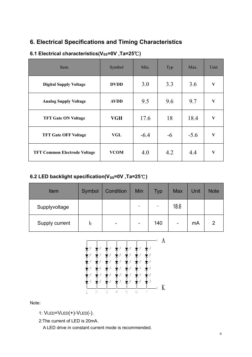
6. Electrical Specifications and Timing Characteristics
6.1 Electrical characteristics(VSS=0V ,Ta=25℃)
Item
Symbol
Min.
Digital Supply Voltage
DVDD
Analog Supply Voltage
TFT Gate ON Voltage
TFT Gate OFF Voltage
AVDD
VGH
VGL
TFT Common Electrode Voltage
VCOM
3.0
9.5
17.6
-6.4
4.0
Typ
3.3
9.6
18
-6
4.2
Max.
Unit
3.6
9.7
18.4
-5.6
4.4
V
V
V
V
V
6.2 LED backlight specification(VSS=0V ,Ta=25℃)
Item
Symbol Condition Min
Typ
Max
Unit
Note
Supplyvoltage
Supply current
If
-
-
-
-
18.6
140
-
mA
2
A
K
Note:
1: VLED=VLED(+)-VLED(-).
2:The current of LED is 20mA.
A LED drive in constant current mode is recommended.
6
�
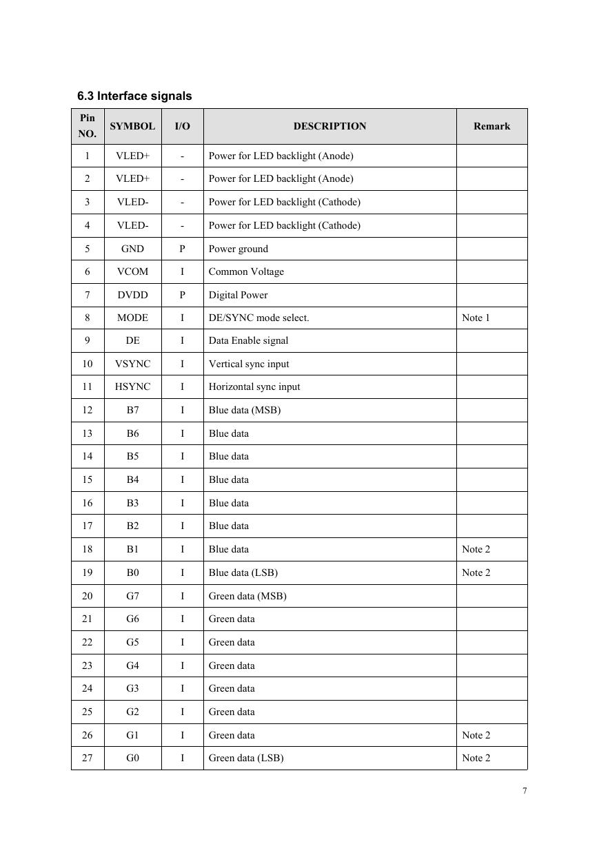
6.3 Interface signals
Pin
NO.
SYMBOL
I/O
1
2
3
4
5
6
7
8
9
10
11
12
13
14
15
16
17
18
19
20
21
22
23
24
25
26
27
VLED+
VLED+
VLED-
VLED-
GND
VCOM
DVDD
MODE
DE
VSYNC
HSYNC
B7
B6
B5
B4
B3
B2
B1
B0
G7
G6
G5
G4
G3
G2
G1
G0
-
-
-
-
P
I
P
I
I
I
I
I
I
I
I
I
I
I
I
I
I
I
I
I
I
I
I
DESCRIPTION
Remark
Power for LED backlight (Anode)
Power for LED backlight (Anode)
Power for LED backlight (Cathode)
Power for LED backlight (Cathode)
Power ground
Common Voltage
Digital Power
DE/SYNC mode select.
Data Enable signal
Vertical sync input
Horizontal sync input
Blue data (MSB)
Blue data
Blue data
Blue data
Blue data
Blue data
Blue data
Blue data (LSB)
Green data (MSB)
Green data
Green data
Green data
Green data
Green data
Green data
Green data (LSB)
Note 1
Note 2
Note 2
Note 2
Note 2
7
�
28
29
30
31
32
33
34
35
36
37
38
39
40
41
42
43
44
45
46
47
48
49
50
R7
R6
R5
R4
R3
R2
R1
R0
GND
DCLK
GND
SHLR
UPDN
VGH
VGL
AVDD
RESET
NC
VCOM
DITH
GND
NC
NC
I
I
I
I
I
I
I
I
P
I
P
I
I
P
P
P
I
-
I
I
P
-
-
Red data (MSB)
Red data
Red data
Red data
Red data
Red data
Red data
Red data (LSB)
Power ground
Clock input
Power ground
Left / Right Selection
Up / Down Selection
Gate ON Voltage
Gate OFF Voltage
Power for Analog Circuit
Global reset pin
Not connection
Common Voltage
Note 2
Note 2
Note 3
Note 4,5
Note 4,5
Note 6
Dithering function enable control
Note 7
Power ground
Not connection
Not connection
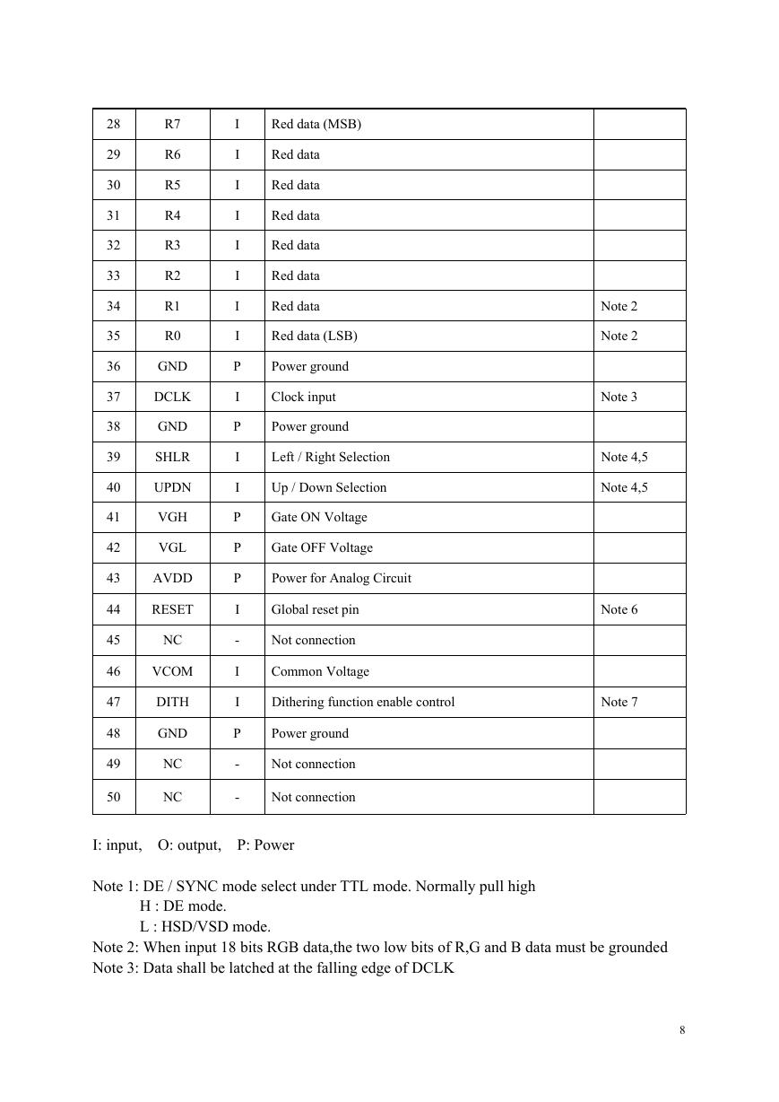
I: input, O: output, P: Power
Note 1: DE / SYNC mode select under TTL mode. Normally pull high
H : DE mode.
L : HSD/VSD mode.
Note 2: When input 18 bits RGB data,the two low bits of R,G and B data must be grounded
Note 3: Data shall be latched at the falling edge of DCLK
8
�



 V2版本原理图(Capacitive-Fingerprint-Reader-Schematic_V2).pdf
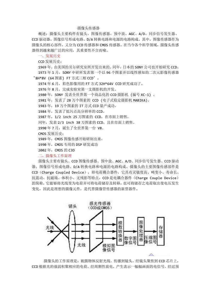 摄像头工作原理.doc
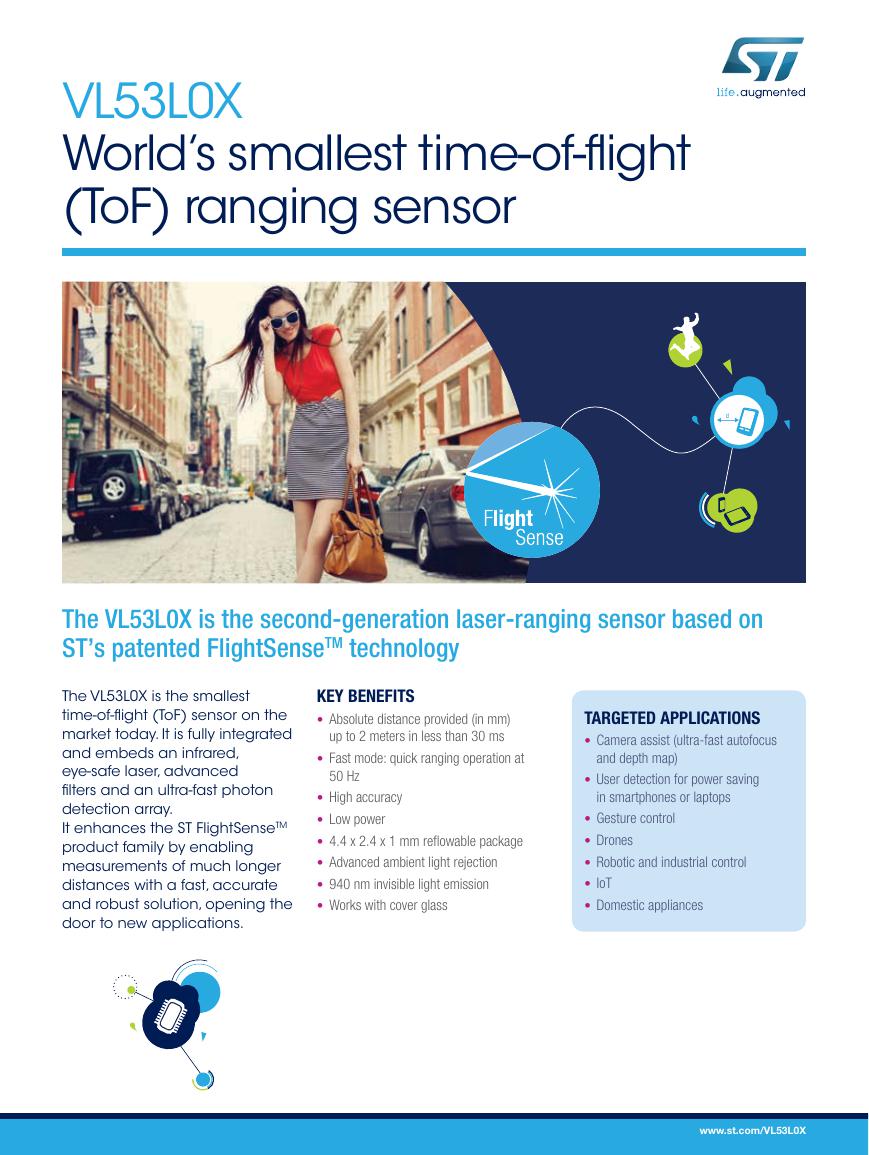 VL53L0X简要说明(En.FLVL53L00216).pdf
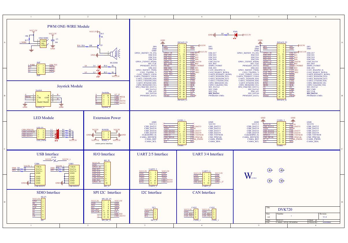 原理图(DVK720-Schematic).pdf
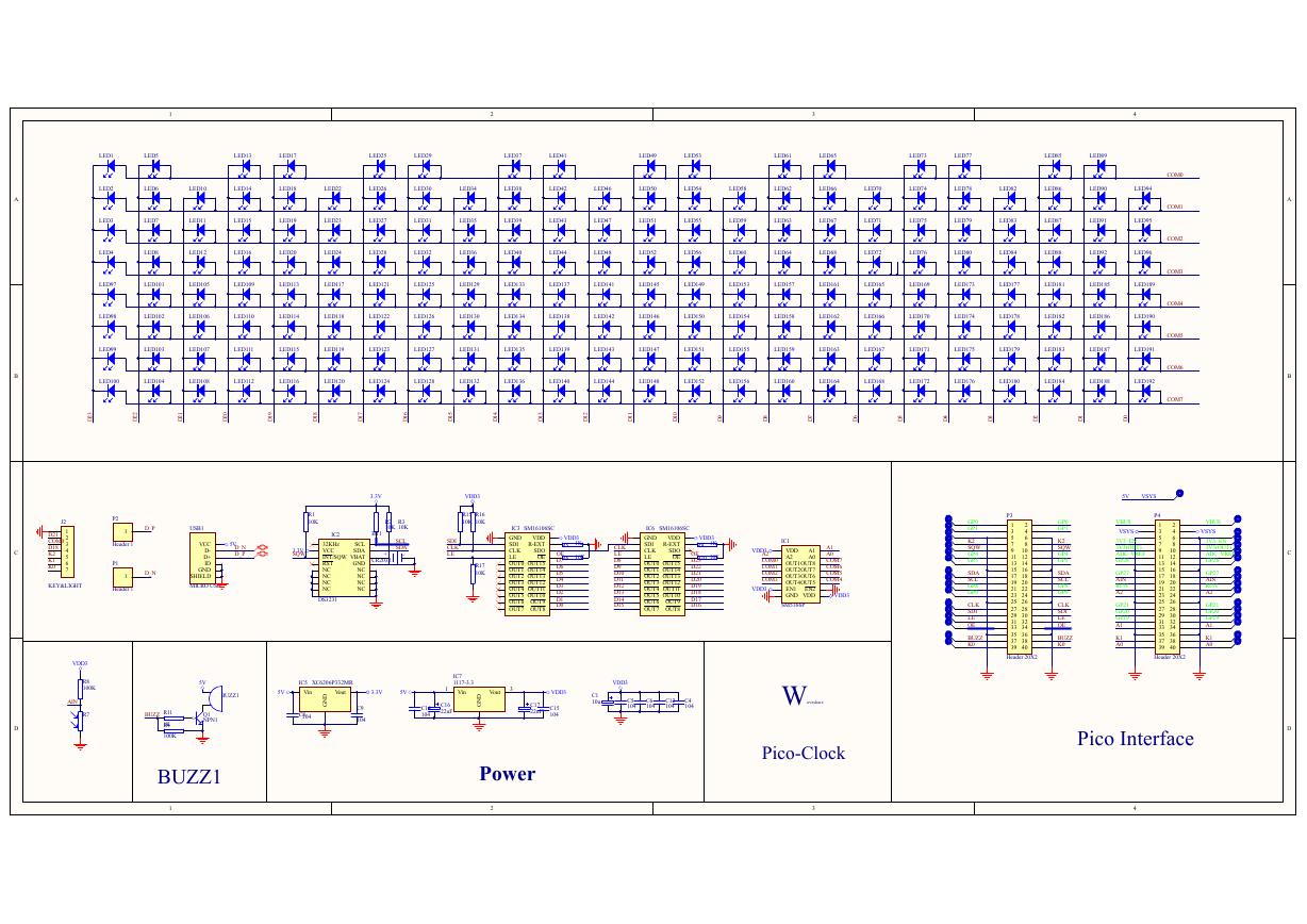 原理图(Pico-Clock-Green-Schdoc).pdf
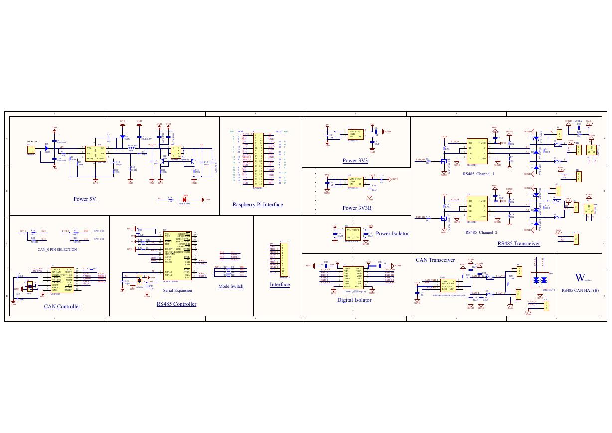 原理图(RS485-CAN-HAT-B-schematic).pdf
 File:SIM7500_SIM7600_SIM7800 Series_SSL_Application Note_V2.00.pdf
 ADS1263(Ads1262).pdf
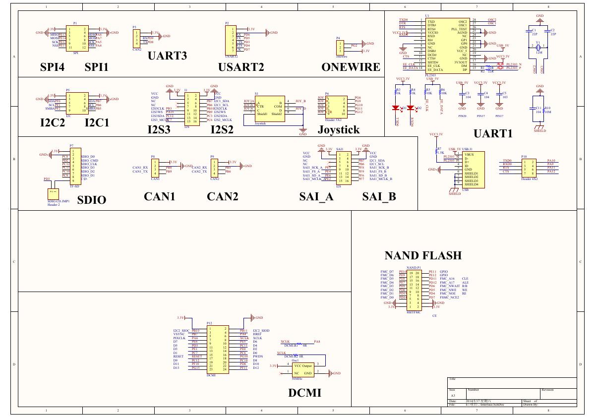 原理图(Open429Z-D-Schematic).pdf
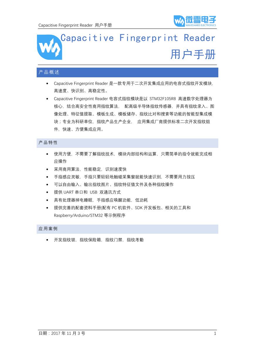 用户手册(Capacitive_Fingerprint_Reader_User_Manual_CN).pdf
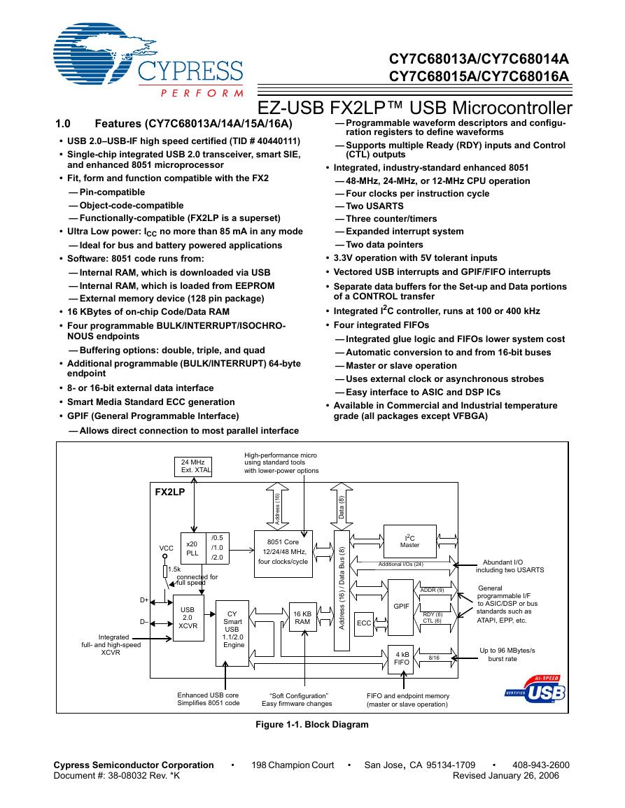 CY7C68013A(英文版)(CY7C68013A).pdf
 TechnicalReference_Dem.pdf