Data Sheet
V 1.0 / Apr. 2017
MSM261S4030H0R
I2S digital output MEMS microphone with Multi‐modes
�
MSM261S4030H0R
I2S digital output MEMS microphone
GENERAL DESCRIPTION
APPLICATIONS
Mobile Phone
Laptop
Tablet computer
Bluetooth headset
Earphone
Wearable intelligent equipment
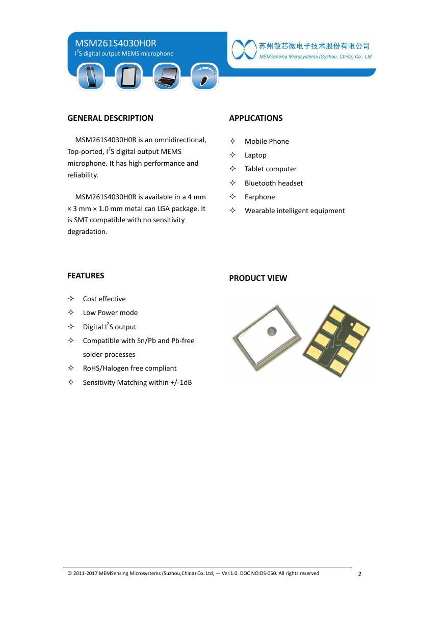
PRODUCT VIEW
MSM261S4030H0R is an omnidirectional,
Top‐ported, I2S digital output MEMS
microphone. It has high performance and
reliability.
MSM261S4030H0R is available in a 4 mm
× 3 mm × 1.0 mm metal can LGA package. It
is SMT compatible with no sensitivity
degradation.
FEATURES
Cost effective
Low Power mode
Digital I2S output
Compatible with Sn/Pb and Pb‐free
solder processes
RoHS/Halogen free compliant
Sensitivity Matching within +/‐1dB
© 2011‐2017 MEMSensing Microsystems (Suzhou,China) Co. Ltd, — Ver.1.0. DOC NO:DS‐050. All rights reserved
2
�
MSM261S4030H0R
I2S digital output MEMS microphone
ABSOLUTE MAXIMUM RATINGS
Parameter
Supply Voltage
Sound Pressure Level
Mechanical Shock
Temperature Range
Electrostatic discharge protection
SPECIFICATIONS
Maximum value
−0.3 to 4.0
140
10,000
−40 to 100
2 (HBM)
Unit
V
dB SPL
g
°C
kV
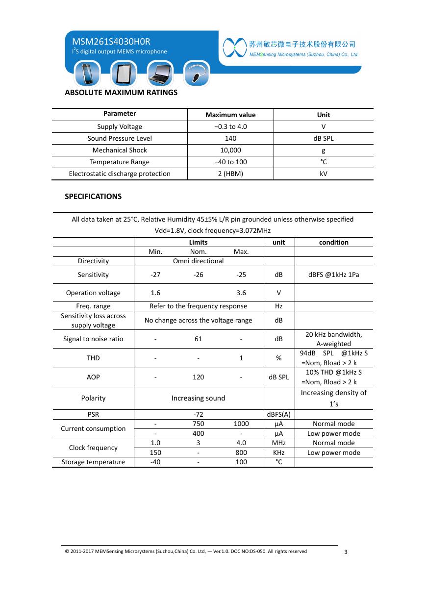
All data taken at 25°C, Relative Humidity 45±5% L/R pin grounded unless otherwise specified
Directivity
Sensitivity
Operation voltage
Freq. range
Sensitivity loss across
supply voltage
Vdd=1.8V, clock frequency=3.072MHz
Limits
Nom.
Omni directional
‐26
Min.
‐27
Max.
‐25
1.6
3.6
Refer to the frequency response
No change across the voltage range
Signal to noise ratio
THD
AOP
Polarity
PSR
Current consumption
Clock frequency
Storage temperature
‐
‐
‐
‐
‐
1.0
150
‐40
61
‐
120
Increasing sound
‐72
750
400
3
‐
‐
‐
1
‐
1000
‐
4.0
800
100
unit
dB
V
Hz
dB
dB
%
dB SPL
dBFS(A)
μA
μA
MHz
KHz
°C
condition
dBFS @1kHz 1Pa
20 kHz bandwidth,
A‐weighted
94dB SPL @1kHz S
=Nom, Rload > 2 k
10% THD @1kHz S
=Nom, Rload > 2 k
Increasing density of
1’s
Normal mode
Low power mode
Normal mode
Low power mode
© 2011‐2017 MEMSensing Microsystems (Suzhou,China) Co. Ltd, — Ver.1.0. DOC NO:DS‐050. All rights reserved
3
�
MSM261S4030H0R
I2S digital output MEMS microphone
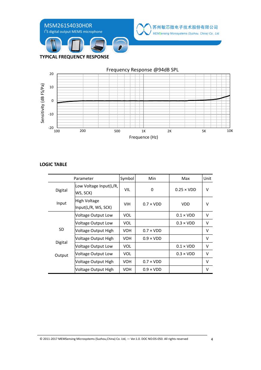
TYPICAL FREQUENCY RESPONSE
Frequency Response @94dB SPL
200
500
1K
2K
5K
Frequence (Hz)
10K
20
10
0
‐10
‐20
100
)
a
P
/
S
F
B
d
(
y
t
i
v
i
t
i
s
n
e
S
LOGIC TABLE
Digital
Input
SD
Digital
Output
Parameter
Low Voltage Input(L/R,
WS, SCK)
High Voltage
Input(L/R, WS, SCK)
Voltage Output Low
Voltage Output Low
Voltage Output High
Voltage Output High
Voltage Output Low
Voltage Output Low
Voltage Output High
Voltage Output High
Symbol
VIL
VIH
VOL
VOL
VOH
VOH
VOL
VOL
VOH
VOH
Min
0
0.7 × VDD
VDD
0.7 × VDD
0.9 × VDD
0.7 × VDD
0.9 × VDD
0.1 × VDD
0.3 × VDD
0.1 × VDD
0.3 × VDD
Max
Unit
0.25 × VDD
V
V
V
V
V
V
V
V
V
V
© 2011‐2017 MEMSensing Microsystems (Suzhou,China) Co. Ltd, — Ver.1.0. DOC NO:DS‐050. All rights reserved
4
�
MSM261S4030H0R
I2S digital output MEMS microphone
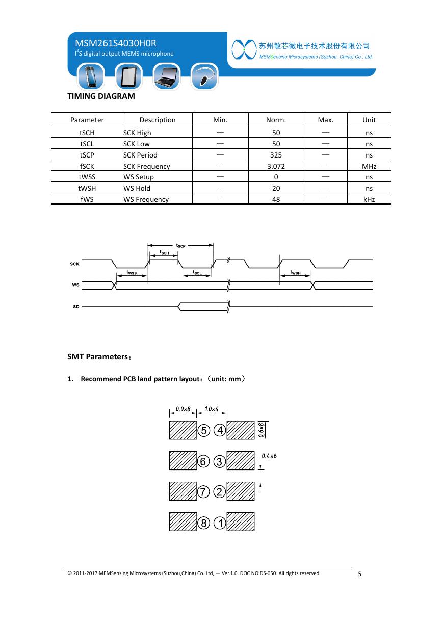
TIMING DIAGRAM
Parameter
Description
tSCH
tSCL
tSCP
fSCK
tWSS
tWSH
fWS
SCK High
SCK Low
SCK Period
SCK Frequency
WS Setup
WS Hold
WS Frequency
Norm.
50
50
325
3.072
0
20
48
Max.
—
—
—
—
—
—
—
Unit
ns
ns
ns
MHz
ns
ns
kHz
Min.
—
—
—
—
—
—
—
SMT Parameters:
1. Recommend PCB land pattern layout:(unit: mm)
© 2011‐2017 MEMSensing Microsystems (Suzhou,China) Co. Ltd, — Ver.1.0. DOC NO:DS‐050. All rights reserved
5
�
MSM261S4030H0R
I2S digital output MEMS microphone
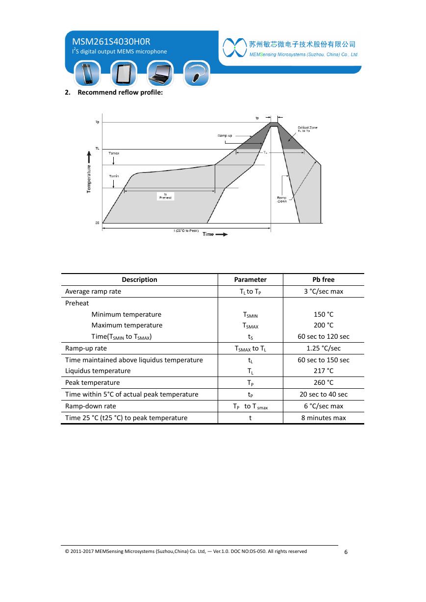
2. Recommend reflow profile:
Description
Average ramp rate
Preheat
Minimum temperature
Maximum temperature
Time(TSMIN to TSMAX)
Ramp‐up rate
Time maintained above liquidus temperature
Liquidus temperature
Peak temperature
Time within 5°C of actual peak temperature
Ramp‐down rate
Time 25 °C (t25 °C) to peak temperature
Pb free
3 °C/sec max
150 °C
200 °C
60 sec to 120 sec
1.25 °C/sec
60 sec to 150 sec
217 °C
260 °C
20 sec to 40 sec
6 °C/sec max
8 minutes max
Parameter
TL to TP
TSMIN
TSMAX
tS
TSMAX to TL
tL
TL
TP
tP
TP to T smax
t
© 2011‐2017 MEMSensing Microsystems (Suzhou,China) Co. Ltd, — Ver.1.0. DOC NO:DS‐050. All rights reserved
6
�
MSM261S4030H0R
I2S digital output MEMS microphone
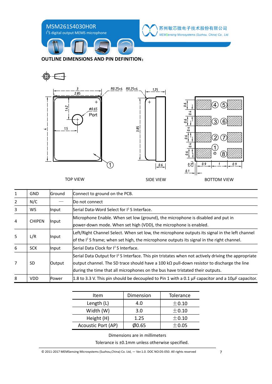
OUTLINE DIMENSIONS AND PIN DEFINITION:
TOP VIEW
SIDE VIEW
BOTTOM VIEW
1
2
3
4
5
6
7
8
GND
N/C
WS
Ground
—
Input
CHIPEN Input
L/R
Input
SCK
Input
SD
Output
Power
VDD
Connect to ground on the PCB.
Do not connect
Serial Data‐Word Select for I²S Interface.
Microphone Enable. When set low (ground), the microphone is disabled and put in
power‐down mode. When set high (VDD), the microphone is enabled.
Left/Right Channel Select. When set low, the microphone outputs its signal in the left channel
of the I²S frame; when set high, the microphone outputs its signal in the right channel.
Serial Data Clock for I²S Interface.
Serial Data Output for I²S Interface. This pin tristates when not actively driving the appropriate
output channel. The SD trace should have a 100 kΩ pull‐down resistor to discharge the line
during the time that all microphones on the bus have tristated their outputs.
1.8 to 3.3 V. This pin should be decoupled to Pin 1 with a 0.1 μF capacitor and a 10μF capacitor.
Item
Length (L)
Width (W)
Height (H)
Acoustic Port (AP)
Dimension
4.0
3.0
1.25
Ø0.65
Tolerance
±0.10
±0.10
±0.10
±0.05
Dimensions are in millimeters
Tolerance is ±0.1mm unless otherwise specified.
© 2011‐2017 MEMSensing Microsystems (Suzhou,China) Co. Ltd, — Ver.1.0. DOC NO:DS‐050. All rights reserved
7
�
MSM261S4030H0R
I2S digital output MEMS microphone
ADDITIONAL NOTES
(A) MSL (moisture sensitivity level) Class 2a.
(B) Maximum of 3 reflow cycles is recommended.
(C) In order to minimize device damage:
Do not board wash or clean after the reflow process.
Do not brush board with or without solvents after the reflow process.
Do not directly expose to ultrasonic processing, welding, or cleaning.
Do not insert any object in port hole of device at any time.
Do not apply air pressure into the port hole.
Do not pull a vacuum over port hole of the microphone.
MATERIALS STATEMENT
Meets the requirements of the European RoHS and Halogen‐Free.
© 2011‐2017 MEMSensing Microsystems (Suzhou,China) Co. Ltd, — Ver.1.0. DOC NO:DS‐050. All rights reserved
8
�


 V2版本原理图(Capacitive-Fingerprint-Reader-Schematic_V2).pdf
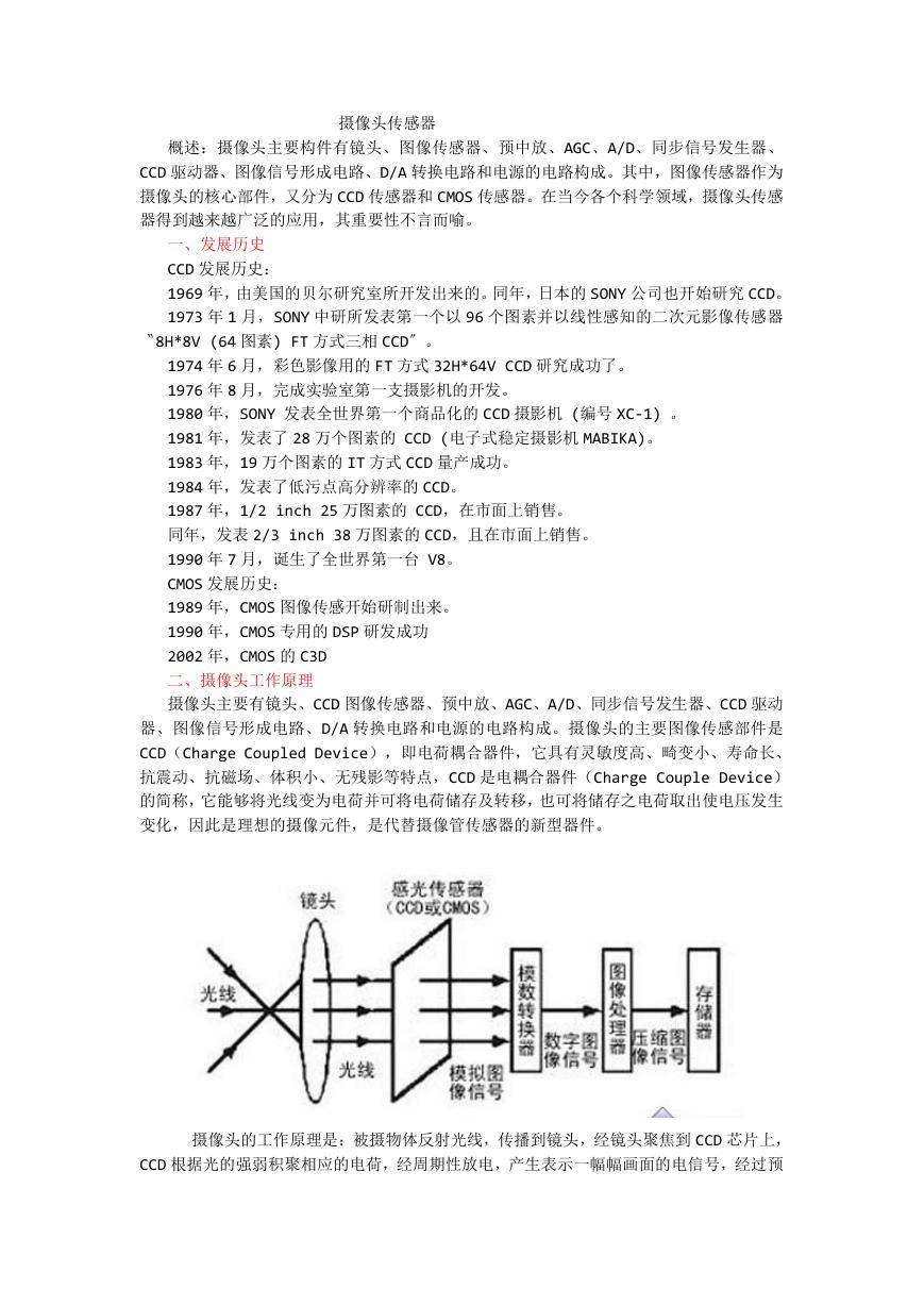 摄像头工作原理.doc
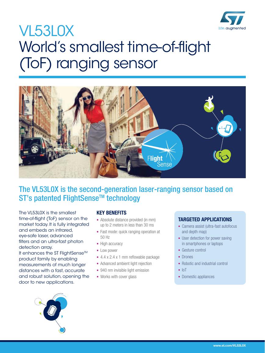 VL53L0X简要说明(En.FLVL53L00216).pdf
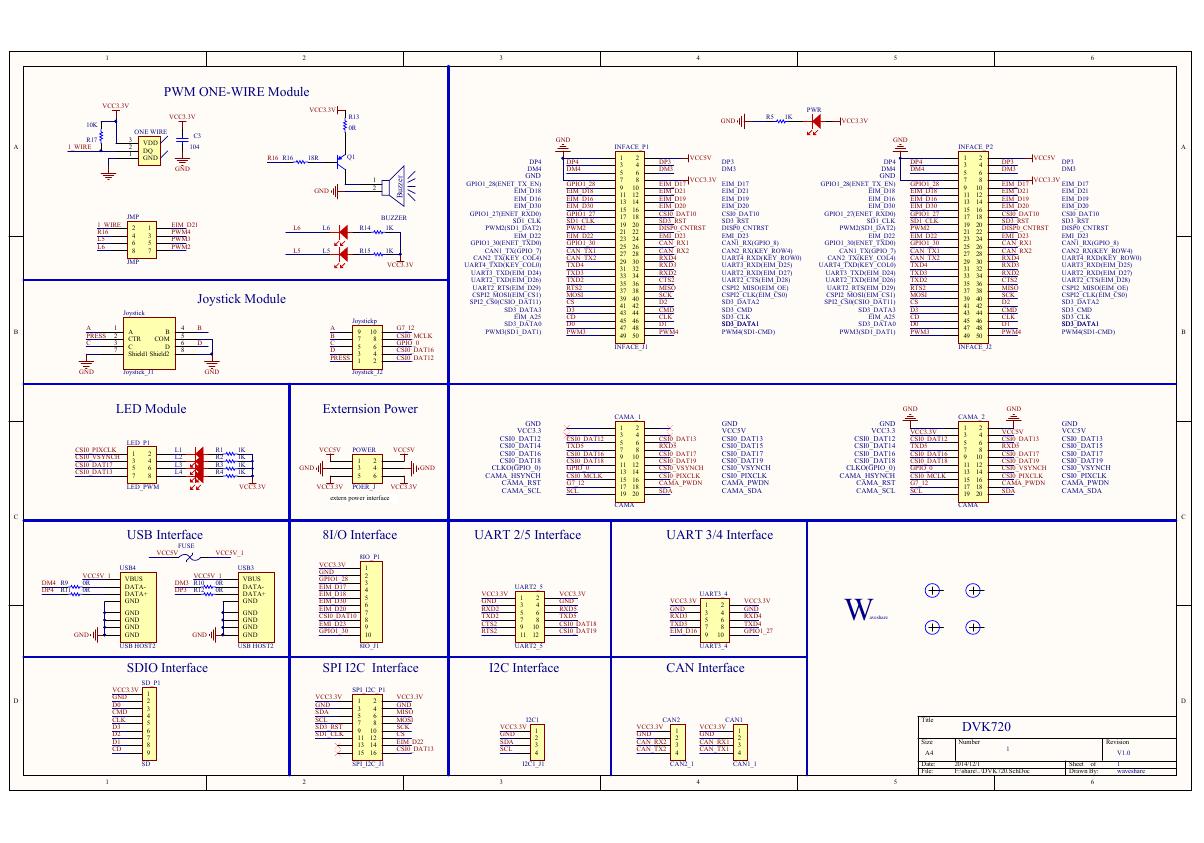 原理图(DVK720-Schematic).pdf
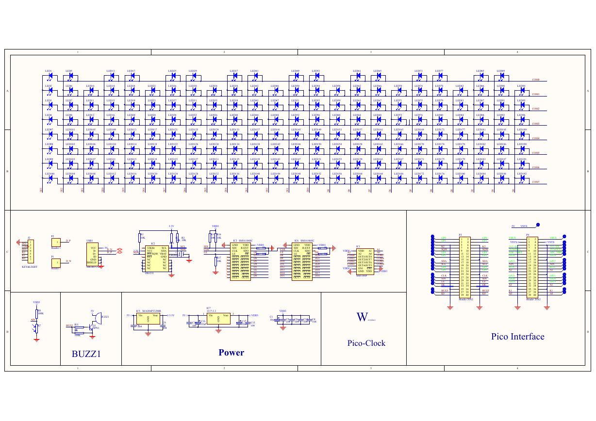 原理图(Pico-Clock-Green-Schdoc).pdf
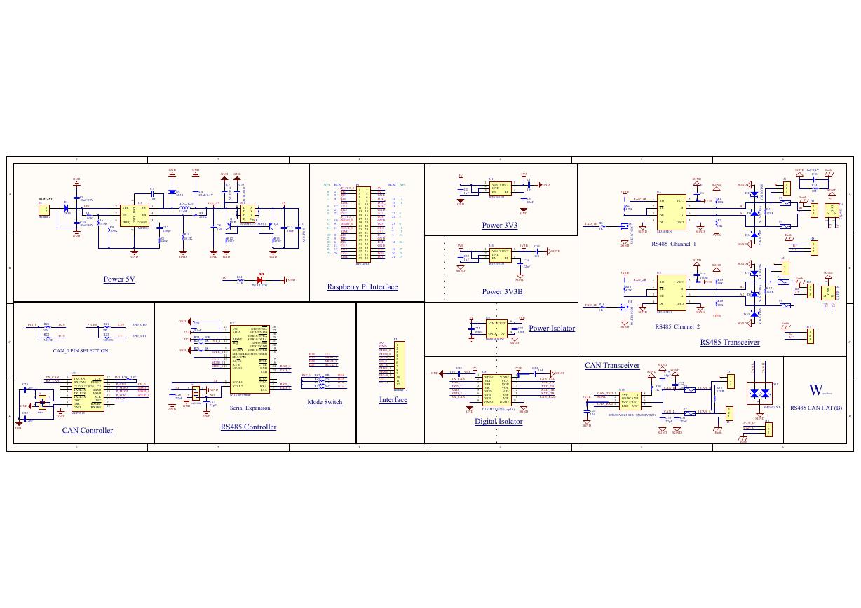 原理图(RS485-CAN-HAT-B-schematic).pdf
 File:SIM7500_SIM7600_SIM7800 Series_SSL_Application Note_V2.00.pdf
 ADS1263(Ads1262).pdf
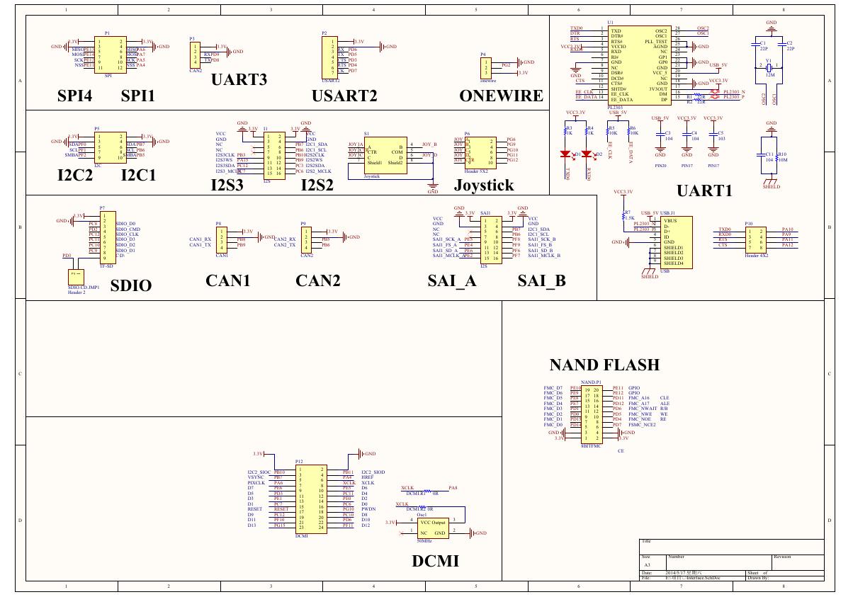 原理图(Open429Z-D-Schematic).pdf
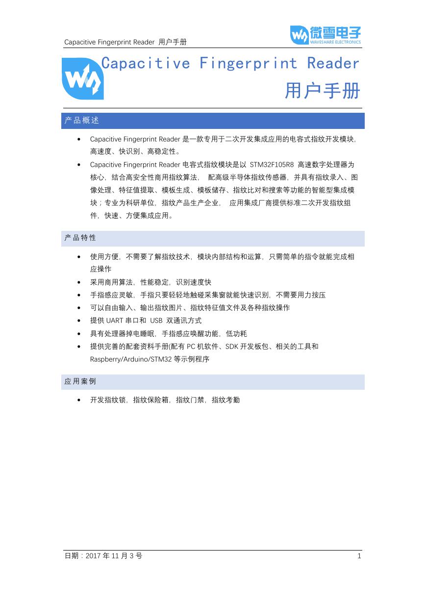 用户手册(Capacitive_Fingerprint_Reader_User_Manual_CN).pdf
 CY7C68013A(英文版)(CY7C68013A).pdf
 TechnicalReference_Dem.pdf