HIGH-VOLTAGE MIXED-SIGNAL IC
All-in-one driver IC w/ Timing Controller for
White/Black/Red Dot-Matrix Micro-Cup ESL
Preliminary Specifications
Datasheet Revision: 0.1
IC Version: c_A
April 1, 2015
S p e c i f i c a t i o n s a n d i n f o r m a t i o n h e r e i n a r e s u b j e c t t o c h a n g e w i t h o u t n o t i c e .
UUUULTRALTRALTRALTRACCCCHIPHIPHIPHIP
The Coolest EPD Driver, Ever!
�
UUUULTRALTRALTRALTRACCCCHIPHIPHIPHIP
©1999~2015
Table of Content
UC8176c_A0.1
All-in-one driver IC w/ Timing Controller
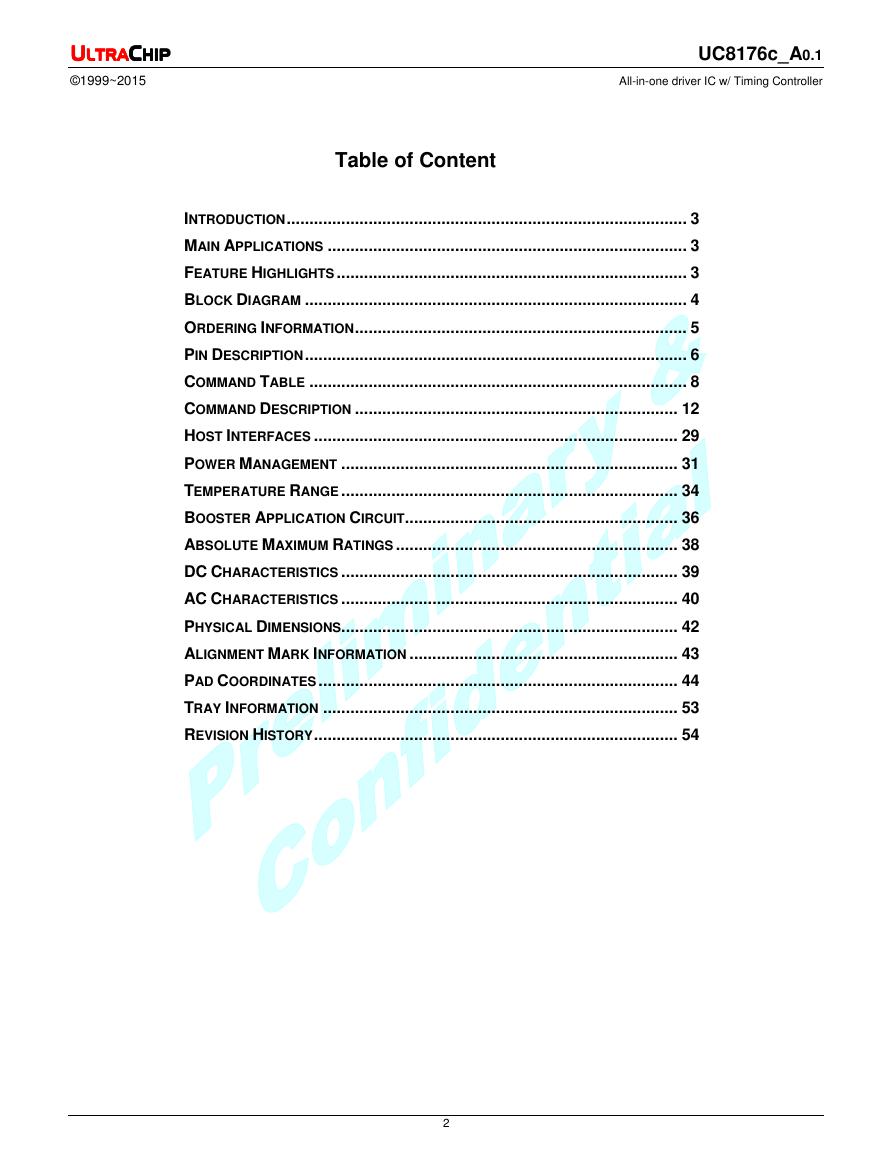
INTRODUCTION........................................................................................ 3
MAIN APPLICATIONS ............................................................................... 3
FEATURE HIGHLIGHTS ............................................................................. 3
BLOCK DIAGRAM .................................................................................... 4
ORDERING INFORMATION......................................................................... 5
PIN DESCRIPTION .................................................................................... 6
COMMAND TABLE ................................................................................... 8
COMMAND DESCRIPTION ....................................................................... 12
HOST INTERFACES ................................................................................ 29
POWER MANAGEMENT .......................................................................... 31
TEMPERATURE RANGE .......................................................................... 34
BOOSTER APPLICATION CIRCUIT............................................................ 36
ABSOLUTE MAXIMUM RATINGS .............................................................. 38
DC CHARACTERISTICS .......................................................................... 39
AC CHARACTERISTICS .......................................................................... 40
PHYSICAL DIMENSIONS.......................................................................... 42
ALIGNMENT MARK INFORMATION ........................................................... 43
PAD COORDINATES ............................................................................... 44
TRAY INFORMATION .............................................................................. 53
REVISION HISTORY................................................................................ 54
2
�
UUUULTRALTRALTRALTRACCCCHIPHIPHIPHIP
©1999~2015
UC8176c_A0.1
All-in-one driver IC w/ Timing Controller
UC8176
All-in-one driver IC with Timing Controller for
Whte/Black/Red Dot-Matrix Micro-Cup ESL
INTRODUCTION
This driver is an all-in-one driver with timing controller for
ESL. Its output is of 1-bit white/black and 1-bit red resolution
per pixel. The timing controller provides control signals for
the source driver and gate drivers.
The DC-DC controller allows it to generate the source
output voltage VDH/VDL (+/-2.4V~+/-11V). The chip also
includes an output buffer for the supply of the COM
electrode
is
configurable through a 3-wire/4-wire (SPI) serial interface.
(VCOMAC or VCOMDC). The system
MAIN APPLICATIONS
• E-tag application
FEATURE HIGHLIGHTS
• System-on-chip (SOC) for ESL
•
Temperature sensor:
− On-Chip: -25~50 oC +/- 2.0oC / 8-bit status
− Off-Chip: -55~125oC +/- 2.0oC /11-bit status
(I2C/LM75)
• Support LPD, Low Power Detection (VDD<2.5V)
• OSC / PLL: On-chip RC oscillator (1.625MHz +/- 5%)
• Vcom:
− AC-Vcom / DC-Vcom (by LUT)
− Support Vcom sensing (6-bit digital status)
• Charge Pump: On-chip booster and regulator:
− VGH: +16V
− VGL: -16V
− VDH: +2.4 ~ +11.0V (programmable, black/white)
− VDL: -2.4 ~ -11.0V (programmable, black/white)
− VDHR: +2.4 ~ +11.0V (programmable, red)
•
Timing controller supports several all-resolutions
• Digital supply voltage (VDD/AVDD) : 2.3~ 3.6V
• Resolution:
− Up to 400 source x 300 gate resolution
+ 1 border + 1 Vcom
−
1 bit for white/black and 1 bit for red per pixel
• Cascade: Up to 2 chip cascade mode
• Memory (Max.): 400 x 300 x 2 bits SRAM
•
3-wire/4-wire (SPI) serial interface
− Clock rate up to 20MHz
• OTP: 4K-byte OTP for LUT
• Package: (TBD)
• COM/SEG bump information
(TBD) µM
(TBD) µM +/- 3µM
Bump pitch:
Bump gap:
Bump surface: (TBD) µM2
Remark: Contact UltraChip for a visual inspection
document (03-DOC-093).
3
�
UUUULTRALTRALTRALTRACCCCHIPHIPHIPHIP
©1999~2015
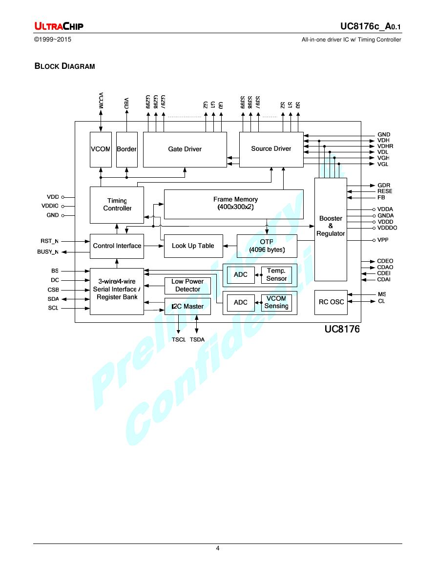
BLOCK DIAGRAM
UC8176c_A0.1
All-in-one driver IC w/ Timing Controller
4
�
UUUULTRALTRALTRALTRACCCCHIPHIPHIPHIP
©1999~2015
UC8176c_A0.1
All-in-one driver IC w/ Timing Controller
ORDERING INFORMATION
Part Number
I2C
Description
General Notes
APPLICATION INFORMATION
For improved readability, the specification contains many application data points. When application information is given, it is advisory and does
not form part of the specification for the device.
BARE DIE DISCLAIMER
All die are tested and are guaranteed to comply with all data sheet limits up to the point of wafer sawing. There is no post waffle saw/pack testing
performed on individual die. Although the latest modern processes are utilized for wafer sawing and die pick-&-place into waffle pack carriers,
UltraChip has no control of third party procedures in the handling, packing or assembly of the die. Accordingly, it is the responsibility of the
customer to test and qualify their application in which the die is to be used. UltraChip assumes no liability for device functionality or performance
of the die or systems after handling, packing or assembly of the die.
LIFE SUPPORT APPLICATIONS
These devices are not designed for use in life support appliances, or systems where malfunction of these products can reasonably be expected to
result in personal injuries. Customer using or selling these products for use in such applications do so at their own risk.
CONTENT DISCLAIMER
UltraChip believes the information contained in this document to be accurate and reliable. However, it is subject to change without notice. No
responsibility is assumed by UltraChip for its use, nor for infringement of patents or other rights of third parties. No part of this publication may be
reproduced, or transmitted in any form or by any means without the prior consent of UltraChip Inc. UltraChip's terms and conditions of sale apply
at all times.
CONTACT DETAILS
UltraChip Inc. (Headquarter)
4F, No. 618, Recom Road,
Neihu District, Taipei 114,
Taiwan, R. O. C.
Tel: +886 (2) 8797-8947
Fax: +886 (2) 8797-8910
Sales e-mail: sales@ultrachip.com
Web site: http://www.ultrachip.com
5
�
UUUULTRALTRALTRALTRACCCCHIPHIPHIPHIP
©1999~2015
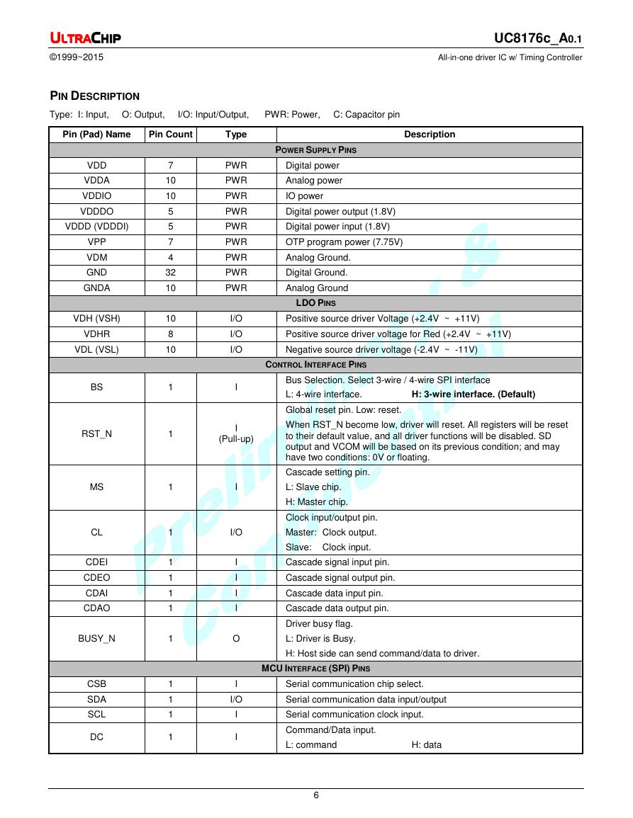
PIN DESCRIPTION
UC8176c_A0.1
All-in-one driver IC w/ Timing Controller
Type: I: Input, O: Output, I/O: Input/Output, PWR: Power, C: Capacitor pin
Pin (Pad) Name
Pin Count
Type
Description
VDD
VDDA
VDDIO
VDDDO
VDDD (VDDDI)
VPP
VDM
GND
GNDA
VDH (VSH)
VDHR
VDL (VSL)
BS
RST_N
MS
CL
CDEI
CDEO
CDAI
CDAO
BUSY_N
CSB
SDA
SCL
DC
7
10
10
5
5
7
4
32
10
10
8
10
1
1
1
1
1
1
1
1
1
1
1
1
1
PWR
PWR
PWR
PWR
PWR
PWR
PWR
PWR
PWR
I/O
I/O
I/O
I
I
(Pull-up)
POWER SUPPLY PINS
Digital power
Analog power
IO power
Digital power output (1.8V)
Digital power input (1.8V)
OTP program power (7.75V)
Analog Ground.
Digital Ground.
Analog Ground
LDO PINS
Positive source driver Voltage (+2.4V ~ +11V)
Positive source driver voltage for Red (+2.4V ~ +11V)
Negative source driver voltage (-2.4V ~ -11V)
CONTROL INTERFACE PINS
Bus Selection. Select 3-wire / 4-wire SPI interface
L: 4-wire interface.
H: 3-wire interface. (Default)
Global reset pin. Low: reset.
When RST_N become low, driver will reset. All registers will be reset
to their default value, and all driver functions will be disabled. SD
output and VCOM will be based on its previous condition; and may
have two conditions: 0V or floating.
Cascade setting pin.
I
L: Slave chip.
H: Master chip.
Clock input/output pin.
I/O
Master: Clock output.
I
I
I
I
Slave: Clock input.
Cascade signal input pin.
Cascade signal output pin.
Cascade data input pin.
Cascade data output pin.
Driver busy flag.
O
L: Driver is Busy.
H: Host side can send command/data to driver.
MCU INTERFACE (SPI) PINS
I
I/O
I
I
Serial communication chip select.
Serial communication data input/output
Serial communication clock input.
Command/Data input.
L: command
H: data
6
�
UUUULTRALTRALTRALTRACCCCHIPHIPHIPHIP
©1999~2015
UC8176c_A0.1
All-in-one driver IC w/ Timing Controller
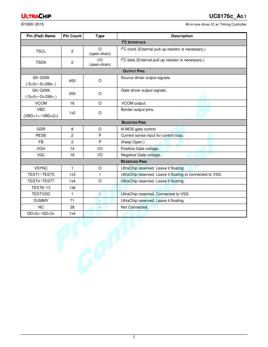
Pin (Pad) Name
Pin Count
Type
Description
I2C INTERFACE
I2C clock (External pull-up resistor is necessary.)
I2C data (External pull-up resistor is necessary.)
O
(open-drain)
I/O
(open-drain)
OUTPUT PINS
Source driver output signals.
Gate driver output signals.
VCOM output.
Border output pins.
BOOSTER PINS
N-MOS gate control
Current sense input for control loop.
(Keep Open.)
Positive Gate voltage.
Negative Gate voltage.
RESERVED PINS
UltraChip reserved. Leave it floating.
UltraChip reserved. Leave it floating or connected to VSS.
UltraChip reserved. Leave it floating.
UltraChip reserved. Connected to VSS.
UltraChip reserved. Leave it floating.
Not Connected.
O
O
O
O
O
P
P
I/O
I/O
O
I
O
I
-
--
TSCL
TSDA
S0~S399
( S<0>~S<399> )
G0~G299
( G<0>~G<299> )
VCOM
VBD
(VBD<1>~VBD<2>)
GDR
RESE
FB
VGH
VGL
VSYNC
TEST1~TEST3
TEST4~TEST7
TEST8~13
TESTVDD
DUMMY
NC
2
2
400
300
16
1x2
8
2
2
14
16
1
1x3
1x4
1x6
1
71
28
GD<0>~GD<3>
1x4
7
�
UUUULTRALTRALTRALTRACCCCHIPHIPHIPHIP
©1999~2015
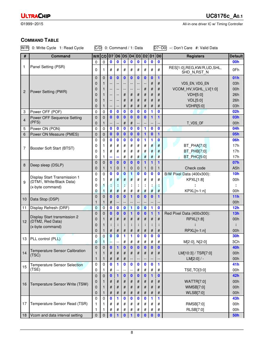
COMMAND TABLE
UC8176c_A0.1
All-in-one driver IC w/ Timing Controller
W/R: 0: Write Cycle 1: Read Cycle C/D: 0: Command / 1: Data D7~D0: –: Don’t Care #: Valid Data
W/R C/D D7 D6 D5 D4 D3 D2 D1 D0
0 0 0 0 0 0 0 0 0
0
1 # # # # # # # #
Registers
Default
RES[1:0],REG,KW/R,UD,SHL,
SHD_N,RST_N
00h
0Fh
01h
03h
00h
26h
26h
03h
02h
03h
00h
04h
05h
06h
17h
17h
17h
07h
A5h
10h
00h
:
00h
11h
00h
12h
13h
00h
:
00h
30h
3Ch
40h
00h
00h
41h
00h
42h
00h
00h
00h
43h
00h
00h
50h
#
Command
1 Panel Setting (PSR)
2 Power Setting (PWR)
3 Power OFF (POF)
4
Power OFF Sequence Setting
(PFS)
5 Power ON (PON)
6 Power ON Measure (PMES)
7 Booster Soft Start (BTST)
8 Deep sleep (DSLP)
9
Display Start Transmission 1
(DTM1, White/Black Data)
(x-byte command)
10 Data Stop (DSP)
11 Display Refresh (DRF)
12
Display Start transmission 2
(DTM2, Red Data)
(x-byte command)
13 PLL control (PLL)
14
Temperature Sensor Calibration
(TSC)
15
Temperature Sensor Selection
(TSE)
16 Temperature Sensor Write (TSW)
17 Temperature Sensor Read (TSR)
18 Vcom and data interval setting
0
0
0
0
0
0
0
0
0
0
0
0
0
0
0
0
0
0
0
0
0
0
0
1
0
0
0
0
0
0
0
0
1
1
0
0
0
0
0
0
0
1
1
0
0 0 0 0 0 0 0 0 1
--
--
--
--
--
--
--
-- # #
VDS_EN, VDG_EN
-- # # #
VCOM_HV,VGHL_LV[1:0]
1
1
1
1
--
--
--
--
-- # # # # # #
-- # # # # # #
--
1
-- # # # # # #
0 0 0 0 0 0 0 1 0
0 0 0 0 0 0 0 1 1
--
--
--
--
-- # #
1
--
0 0 0 0 0 0 1 0 0
0 0 0 0 0 0 1 0 1
0 0 0 0 0 0 1 1 0
1 # # # # # # # #
1 # # # # # # # #
-- # # # # # #
1
0 0 0 0 0 0 1 1 1
--
VDH[5:0]
VDL[5:0]
VDHR[5:0]
T_VDS_OF
BT_PHA[7:0]
BT_PHB[7:0]
BT_PHC[5:0]
1 1 0 1 0 0 1 0 1
0 0 0 0 1 0 0 0 0 B/W Pixel Data (400x300):
Check code
1 # # # # # # # #
:
:
:
:
:
:
:
:
1
1 # # # # # # # #
0 0 0 0 1 0 0 0 1
KPXL[1:8]
:
KPXL[n-1:n]
--
--
--
1 #
--
0 0 0 0 1 0 0 1 0
0 0 0 0 1 0 0 1 1 Red Pixel Data (400x300):
--
--
--
1 # # # # # # # #
:
:
:
:
:
:
:
:
1
1 # # # # # # # #
0 0 0 1 1 0 0 0 0
--
1
-- # # # # # #
0 0 1 0 0 0 0 0 0
RPXL[1:8]
:
RPXL[n-1:n]
M[2:0], N[2:0]
1 # # # # # # # #
LM[10:3] / TSR[7:0]
1 # # #
--
0 0 1 0 0 0 0 0 1
--
--
--
--
--
1 #
-- # # # #
0 0 1 0 0 0 0 1 0
--
1 # # # # # # # #
1 # # # # # # # #
1 # # # # # # # #
0 0 1 0 0 0 0 1 1
1 # # # # # # # #
1 # # # # # # # #
0 0 1 0 1 0 0 0 0
8
LM[2:0] / -
TSE,TO[3:0]
WATTR[7:0]
WMSB[7:0]
WLSB[7:0]
RMSB[7:0]
RLSB[7:0]
�



 V2版本原理图(Capacitive-Fingerprint-Reader-Schematic_V2).pdf
 摄像头工作原理.doc
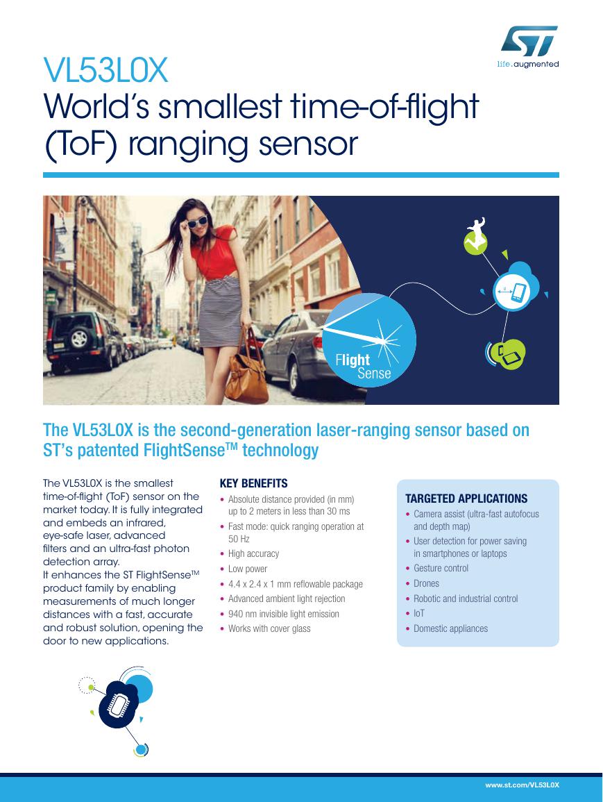 VL53L0X简要说明(En.FLVL53L00216).pdf
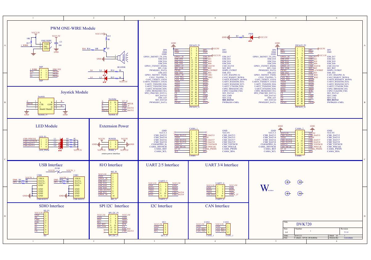 原理图(DVK720-Schematic).pdf
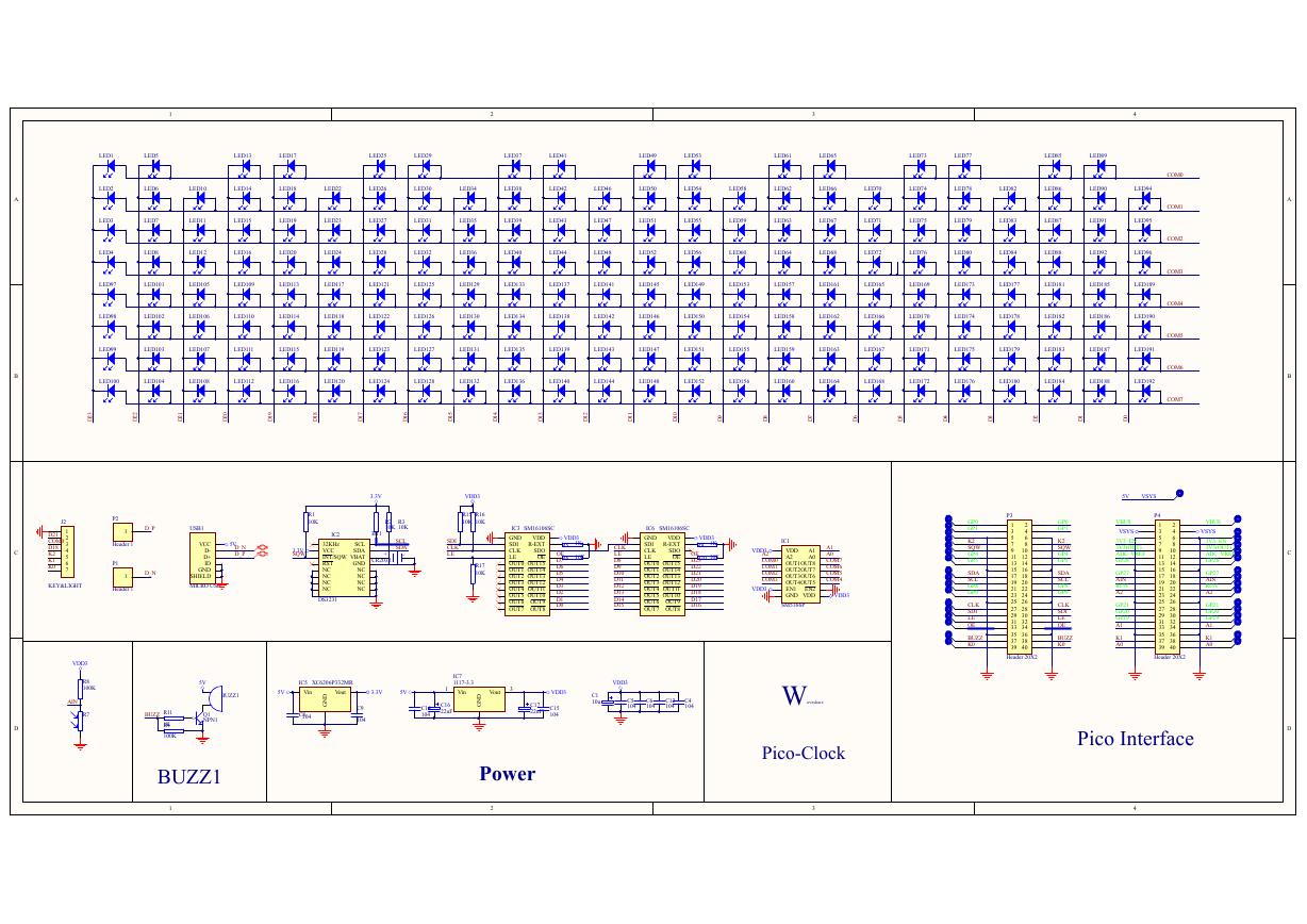 原理图(Pico-Clock-Green-Schdoc).pdf
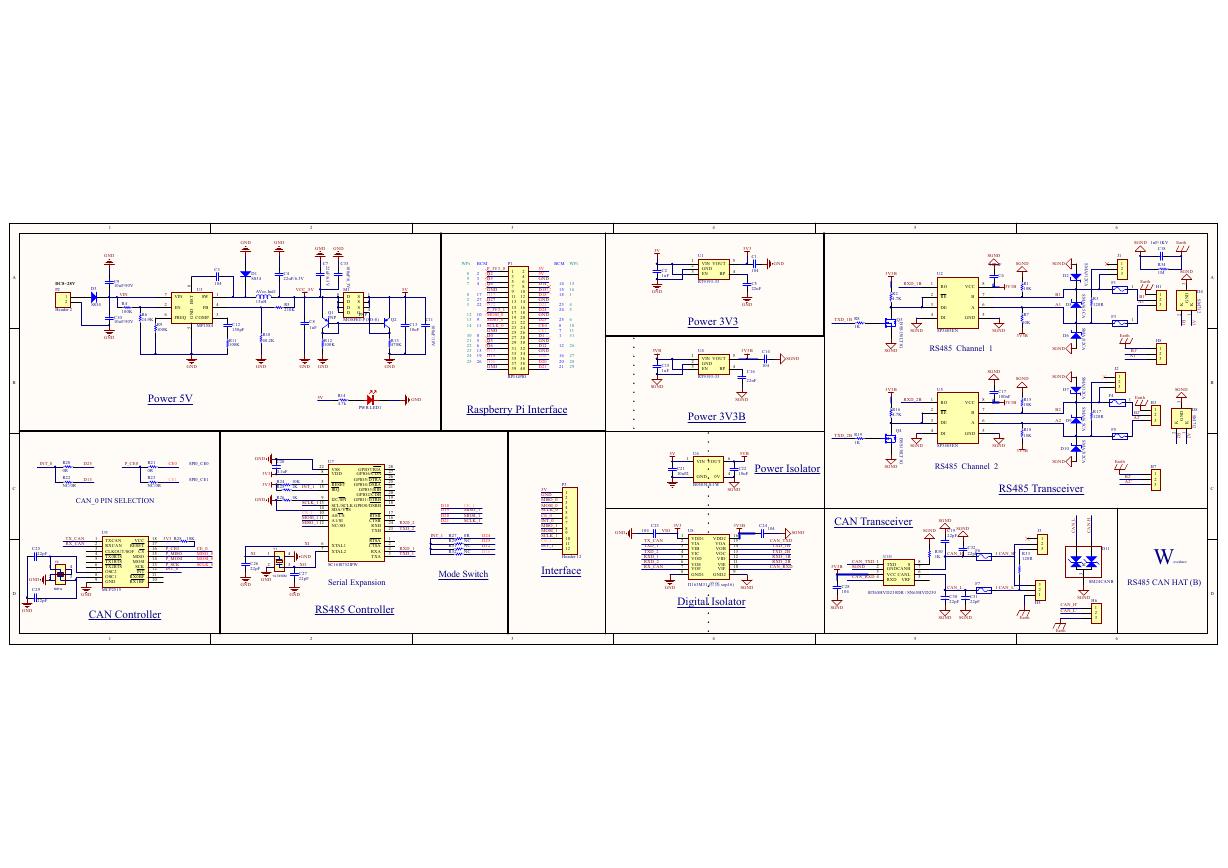 原理图(RS485-CAN-HAT-B-schematic).pdf
 File:SIM7500_SIM7600_SIM7800 Series_SSL_Application Note_V2.00.pdf
 ADS1263(Ads1262).pdf
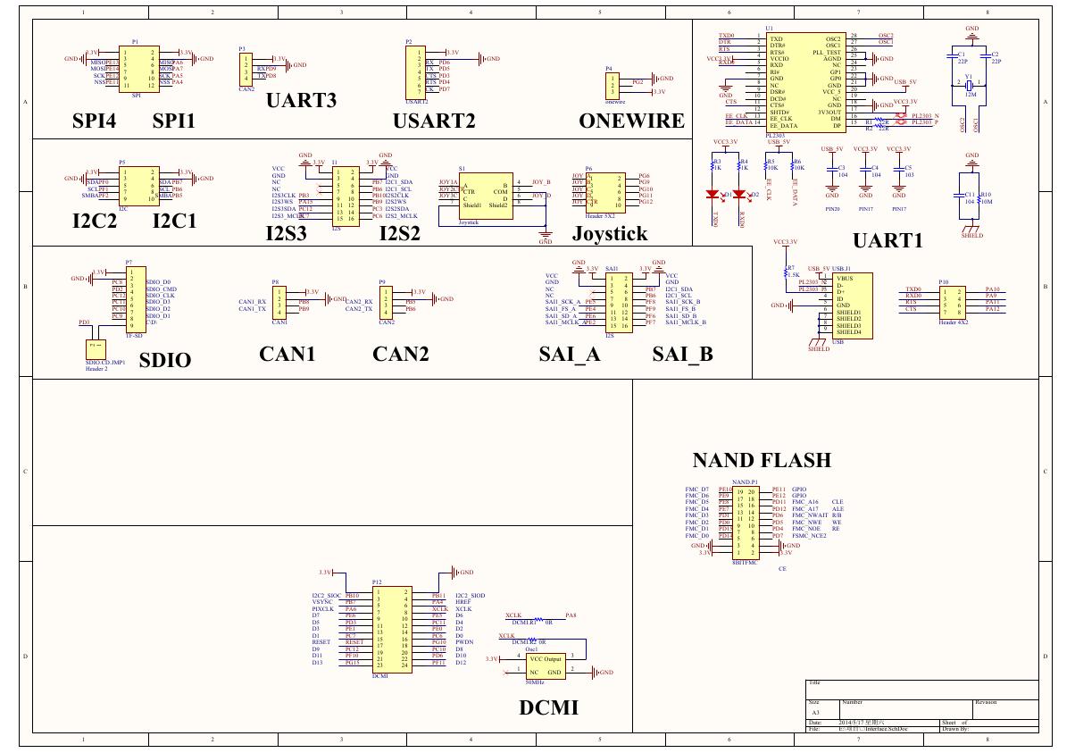 原理图(Open429Z-D-Schematic).pdf
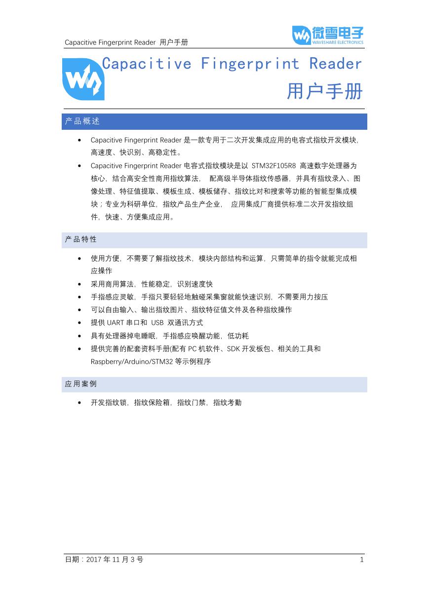 用户手册(Capacitive_Fingerprint_Reader_User_Manual_CN).pdf
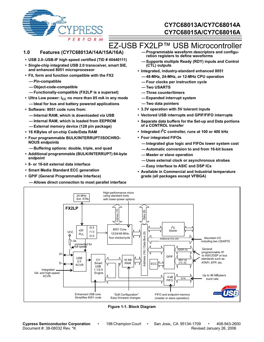 CY7C68013A(英文版)(CY7C68013A).pdf
 TechnicalReference_Dem.pdf