Notes:
Product Specification
Part Name: 1.5inch OLED Display Module
Ver: B
Customer:
Approved by
From:
Approved by
contact Waveshare Electronics
specification
1. Please
module
our products.
problems that may result from application based on the module described herein.
No responsibility is assumed by
Waveshare.
Co.,Ltd.
before
assigning
2. The information contained herein is presented merely to indicate the characteristics and performance of
your
product
based
on
this
for any intellectual property
claims or other
1.5inch OLED Module1 / 32
�
RReevviisseedd HHiissttoorryy
Part Number
Revision
Revision Content
Revised on
A
B
New
修改偏光片尺寸
20220415
20220701
1.5inch OLED B
i
1.5inch OLED Module2 / 32�
CCoonntteennttss
RReevviissiioonn HHiissttoorryy
CCoonntteennttss
11.. BBaassiicc SSppeecciiffiiccaattiioonnss
1.1 Display Specifications
1.2 Mechanical Specifications
1.3 Active Area / Memory Mapping & Pixel Construction
1.4 Mechanical Drawing
1.5 Pin Definition
22.. AAbbssoolluuttee MMaaxxiimmuumm RRaattiinnggss
33.. Optics & EElleeccttrriiccaall CChhaarraacctteerriissttiiccss
3.1 Optics Characteristics
3.2 DC Characteristics
3.3 AC Characteristics
3.3.1 68XX-Series MPU Parallel Interface Characteristics
3.3.2 80XX-Series MPU Parallel Interface Characteristics
3.3.3 Serial Interface Characteristics (4-wire SPI)
3.3.4 I2C Interface Characteristics
44.. FFuunnccttiioonnaall SSppeecciiffiiccaattiioonn
4.1 Commands
4.2 Power down and Power up Sequence
4.2.1 Power up Sequence
4.2.2 Power down Sequence
4.3 Reset Circuit
4.4 Actual Application Example
4.4.1 VCC Supplied Externally
55.. RReelliiaabbiilliittyy
5.1 Contents of Reliability Tests
5.2 Failure Check Standard
66.. OOuuttggooiinngg QQuuaalliittyy CCoonnttrrooll SSppeecciiffiiccaattiioonnss
6.1 Environment Required
6.2 Sampling Plan
6.3 Criteria & Acceptable Quality Level
6.3.1 Cosmetic Check (Display Off) in Non-Active Area
6.3.2 Cosmetic Check (Display Off) in Active Area
6.3.3 Pattern Check (Display On) in Active Area
77.. PPaacckkaaggee SSppeecciiffiiccaattiioonnss
88.. PPrreeccaauuttiioonnss WWhheenn UUssiinngg TThheessee OOEELL DDiissppllaayy MMoodduulleess
8.1 Handling Precautions
8.2 Storage Precautions
8.3 Designing Precautions
8.4 Precautions when disposing of the OEL display modules
8.5 Other Precautions
WWaarrrraannttyy
NNoottiiccee
ii
1.5inch OLED Module3 / 32�
11.. BBaassiicc SSppeecciiffiiccaattiioonnss
1.1 Display Specifications
1) Display Mode:
2) Display Color:
3) Drive Duty:
Passive Matrix
Monochrome (White)
1/128 Duty
1.2 Mechanical Specifications
1) Outline Drawing:
2) Number of Pixels:
3) Panel Size:
4) Active Area:
5) Pixel Pitch:
6) Pixel Size:
7) Weight:
According to the annexed outline drawing
128 128
33.9 37.3 1.44 (mm)
26.855 26.855 (mm)
0.21 0.21 (mm)
0.185 0.185 (mm)
TBD
1.3 Active Area / Memory Mapping & Pixel Construction
SEG 0SEG 126COM0COM127SEG127SEG1"A"---Dots Detailscale 10XG:0.025W:0.185P:0.210G:0.025W:0.185P:0.2101.5inch OLED Module4 / 32�
1
4
.
M
e
c
h
a
n
i
c
a
l
D
r
a
w
n
g
i
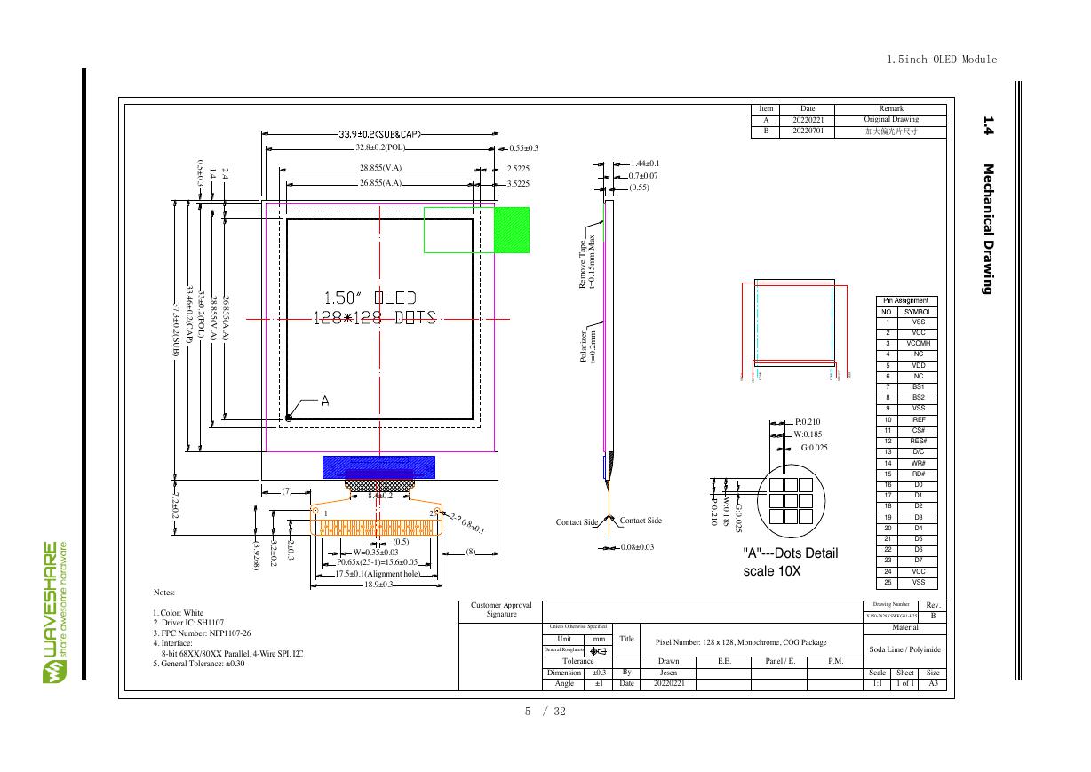
Notes:1. Color: White2. Driver IC: SH11073. FPC Number: NFP1107-264. Interface: 8-bit 68XX/80XX Parallel, 4-Wire SPI, I2C5. General Tolerance: ±0.30 Pixel Number: 128 x 128, Monochrome, COG Package±0.3mmUnless Otherwise SpecifiedUnitToleranceAngleDimensionGeneral RoughnessTitleDateByDrawnDrawing Number1 of 1SheetMaterialPanel / E.E.E.1:1ScaleA3SizeDateItemRemarkRev.Soda Lime / PolyimideCustomer ApprovalSignature±1BX150-2828KSWKG01-H25Jesen20220221AOriginal DrawingP.M.202202211VSS16D07BS114WR#13D/C12RES#11CS#10IREF3VCOMH2VCC24VCC9VSS5VDD6NC15RD#17D118D219D320D421D522D623D725VSS4NC8BS2(0.55)2.41.42.52253.52251.44±0.10.7±0.0726.855(A.A)28.855(V.A)33.46±0.2(CAP)37.3±0.2(SUB)26.855(A.A)28.855(V.A)"A"---Dots Detailscale 10XG:0.025W:0.185P:0.210G:0.025W:0.185P:0.210481SEG 0SEG 126COM0COM127SEG127SEG118.9±0.3W=0.35±0.03P0.65x(25-1)=15.6±0.057.2±0.2125(3.9268)2-?0.8±0.117.5±0.1(Alignment hole)2±0.33.2±0.2(0.5)8.4±0.2(8)(7)32.8±0.2(POL)33±0.2(POL)0.5±0.30.55±0.3Remove Tapet=0.15mm MaxPolarizert=0.2mmContact SideContact Side0.08±0.0320220701B加大偏光片尺寸1.5inch OLED Module5 / 32�
1.5
Pin Definition
Pin Number
Symbol
I/O
Function
PPoowweerr SSuuppppllyy
2,24
5
1,9,25
VCC
VDD
VSS
P
P
P
Power Supplly for OEL Panell
This is the most positive voltage supply pin of the chip. It must be supplied externally.
Power Supplly for Logiic
This is a voltage supply pin. It must be connected to external source.
Ground of OEL System
This is a ground pin. It also acts as a reference for the logic pins, the OEL driving voltages,
and the analog circuits. It must be connected to external ground.
DDrriivveerr
10
3
IInntteerrffaaccee
CCuurrrreenntt RReeffeerreennccee ffoorr BBrriigghhttnneessss AAddjjuussttmmeenntt
IREF
I
This pin is segment current reference pin. A resistor should be connected
between this pin and VSS. Set the current at 12.5A maximum.
VVoollttaaggee OOuuttppuutt HHiigghh LLeevveell ffoorr CCOOMM SSiiggnnaall
VCOMH
O
This pin is the input pin for the voltage output high level for COM signals. A
capacitor should be connected between this pin and VSS.
7,8
12
11
BS1
BS2
RES#
CS#
I
I
I
13
D/C
I
14
WR#
I
15
RD#
I
16~23
D0~D7
I/O
RReesseerrvvee
Communiicatiing Protocoll Sellect
These pins are MCU interface selection input. See the following table:
8-bit 68XX Parallel
8-bit 80XX Parallel
4-wire SPI
I2C
IM1
IM2
0
1
0
1
1
1
0
0
PPoowweerr RReesseett ffoorr CCoonnttrroolllleerr aanndd DDrriivveerr
This pin is reset signal input. When the pin is low, initialization of the chip is
executed. Keep this pin pull high during normal operation.
CChhiipp SSeelleecctt
This pin is the chip select input. The chip is enabled for MCU communication only
when CS# is pulled low.
Data/Command Controll
This pin is Data/Command control pin. When the pin is pulled high, the input at D7~D0
will be interpreted as display data. When the pin is pulled low, the input at D7~D0 will be
transferred to the command register.
When the pin is pulled high and serial interface mode is selected, the data at SI will be
interpreted as data. When it is pulled low, the data at SI will be
transferred to the command register. In I2C mode, this pin acts as SA0 for slave address
selection.
For detail relationship to MCU interface signals, please refer to the Timing Characteristics
Diagrams.
This is a MPU interface input pad.
When connected to an 8080 MPU, this is active LOW. This pad connects to the 8080
MPU WR
signal. The signals on the data bus are latched at the rising edge of the WR signal.
When connected to a 6800 Series MPU: This is the read/write control signal input
terminal.
When R/W = “H”: Read.
When R/W = “L”: Write.
This is a MPU interface input pad.
When connected to an 8080 series MPU, it is active LOW. This pad is connected to
the RD signal
of the 8080 series MPU, and the data bus is in an output status when this signal is
“L”.
When connected to a 6800 series MPU, this is active HIGH. This is used as an enable
clock input
of the 6800 series MPU.
Seriiall Data Input/Output and cllock
When serial mode is selected, D1 will be the serial data input SI and D0 will be the serial
clock input SCL.
When I2C mode is selected, D1 be the serial data input SDA and D0 is the serial clock
input, SCL.
4,6
NC
-
Reserved Piin
The N.C. pins between function pins are reserved for compatible and flexible design.
1.5inch OLED Module6 / 32�
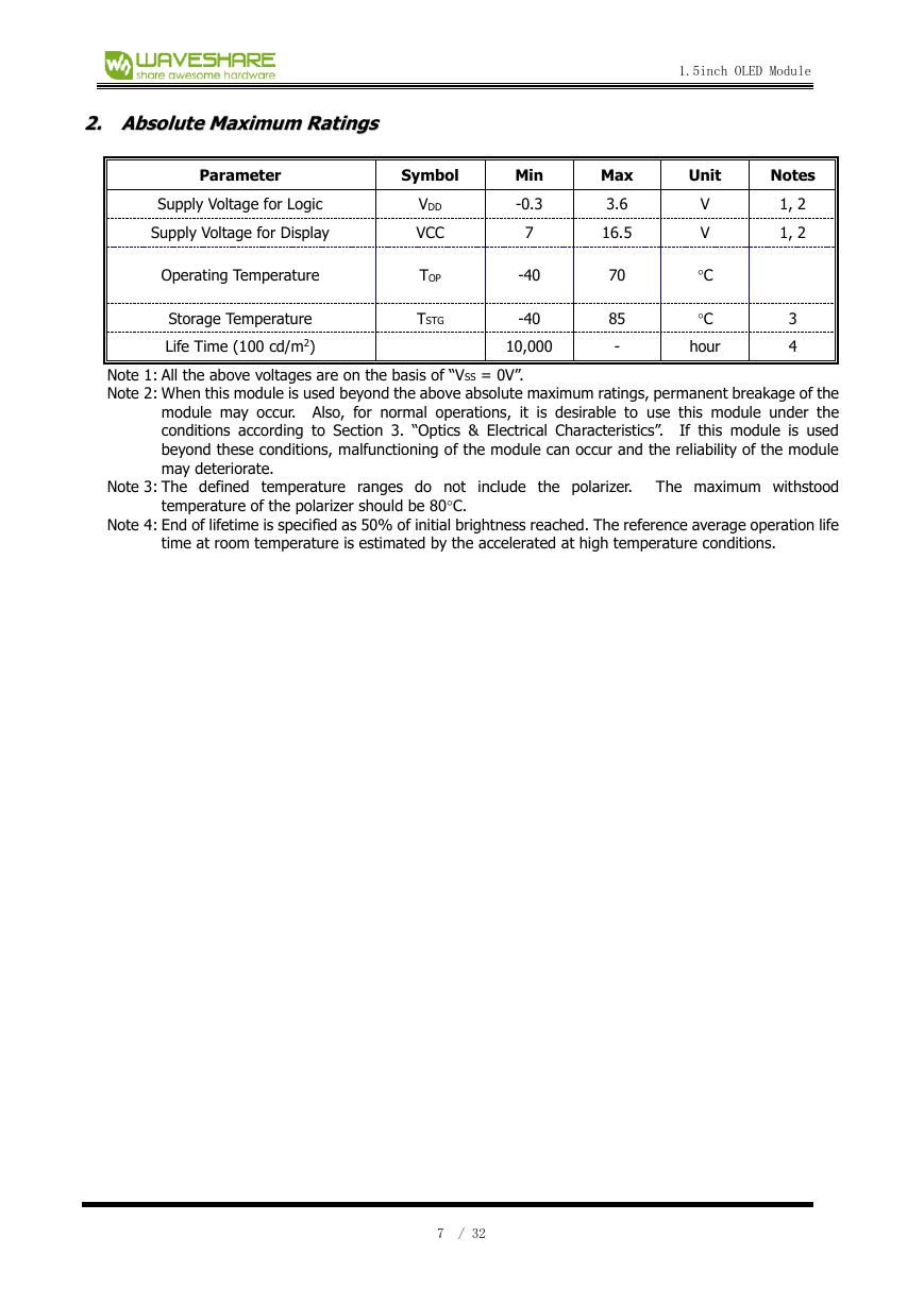
22.. AAbbssoolluuttee MMaaxxiimmuumm RRaattiinnggss
Parameter
Symbol
Supply Voltage for Logic
Supply Voltage for Display
Operating Temperature
Storage Temperature
Life Time (100 cd/m2)
VDD
VCC
TOP
TSTG
Min
-0.3
7
-40
-40
10,000
Max
3.6
16.5
70
85
-
Unit
Notes
V
V
C
C
hour
1, 2
1, 2
3
4
Note 1: All the above voltages are on the basis of “VSS = 0V”.
Note 2: When this module is used beyond the above absolute maximum ratings, permanent breakage of the
module may occur. Also, for normal operations, it is desirable to use this module under the
conditions according to Section 3. “Optics & Electrical Characteristics”. If this module is used
beyond these conditions, malfunctioning of the module can occur and the reliability of the module
may deteriorate.
Note 3: The defined temperature ranges do not include the polarizer. The maximum withstood
temperature of the polarizer should be 80C.
Note 4: End of lifetime is specified as 50% of initial brightness reached. The reference average operation life
time at room temperature is estimated by the accelerated at high temperature conditions.
1.5inch OLED Module7 / 32�
33.. OOppttiiccss && EElleeccttrriiccaall CChhaarraacctteerriissttiiccss
3.1 Optics Characteristics
Characteristics
Symbol
Conditions
Min
Typ
Max
Unit
Brightness
(VCC Supplied Externally)
C.I.E. (White)
Dark Room Contrast
Viewing Angle
Lbr
(x)
(y)
CR
Note 4
80
100
-
cd/m2
C.I.E. 1931
0.25
0.27
0.29
0.31
0.33
0.35
-
-
>10000:1
Free
-
-
degree
* Optical measurement taken at VDD = 2.8V, VCC = 12V.
Software configuration follows Section 4.5 Initialization.
3.2 DC Characteristics
Characteristics
Symbol
Conditions
Min
Typ
Max
Unit
Supply Voltage for Logic
VDD
1.65
2.8
3.5
V
Supply Voltage for Display
VCC
Note 5
11.5
12.0
12.5
V
High Level Input
VIH
IOUT = 100μA, 3.3MHz 0.8VDD
-
VDD
V
Low Level Input
VIL
IOUT = 100μA, 3.3MHz
0
High Level Output
Low Level Output
Operating Current for VCI
Operating Current for VCC
VOH
VOL
IDD
IPP
Sleep Mode Current for VDD IDD, SLEEP
Sleep Mode Current for VCC
ICC, SLEEP
IOUT = 100μA, 3.3MHz 0.8VDD
IOUT = 100μA, 3.3MHz
Note 6
0
-
-
-
-
-
-
-
55
25
0.1
0.5
0.2VDD
VDD
0.2VDD
100
32
5
5
V
V
V
μA
mA
μA
μA
Note 5 & 6: Brightness (Lbr) and Supply Voltage for Display (VCC) are subject to the change of the panel
characteristics and the customer’s request.
Note 6: VDD = 2.8V, VCC = 12.0V, 100% Display Area Turn on.
* Software configuration follows Section 4.5 Initialization.
1.5inch OLED Module8 / 32�






 V2版本原理图(Capacitive-Fingerprint-Reader-Schematic_V2).pdf
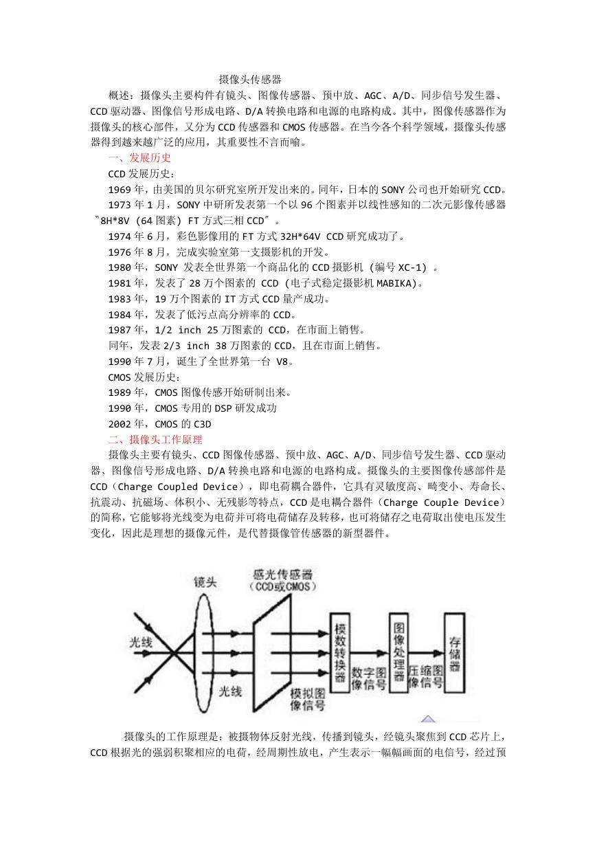 摄像头工作原理.doc
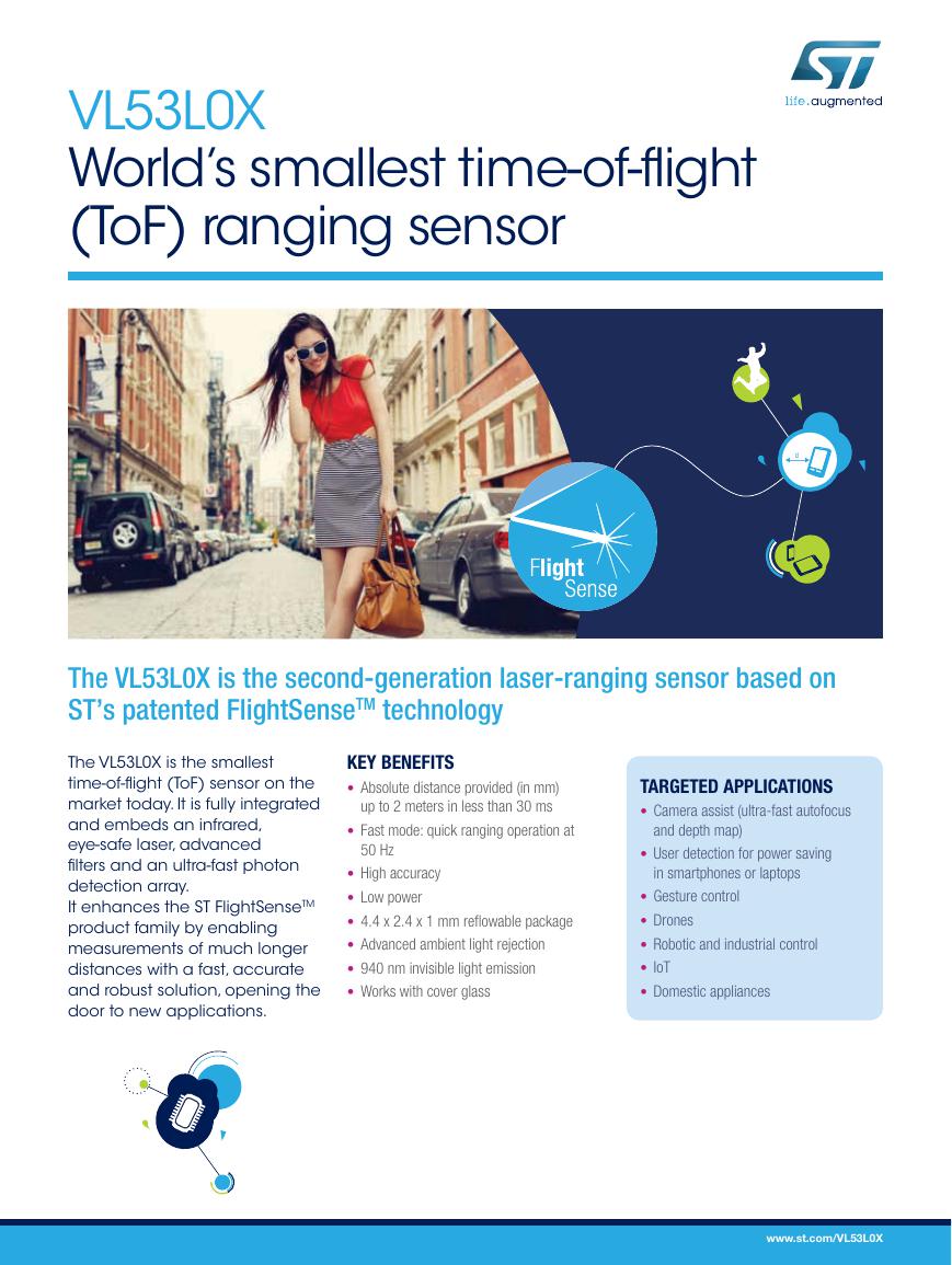 VL53L0X简要说明(En.FLVL53L00216).pdf
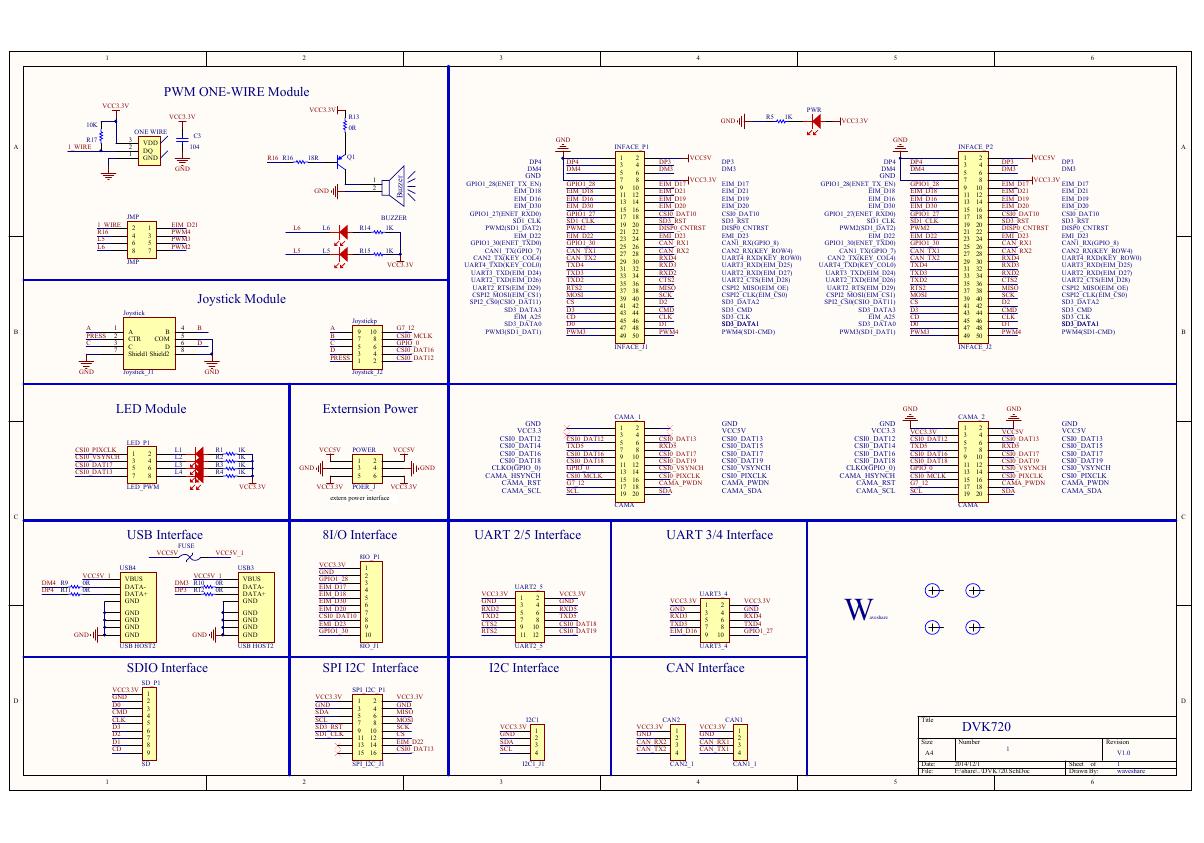 原理图(DVK720-Schematic).pdf
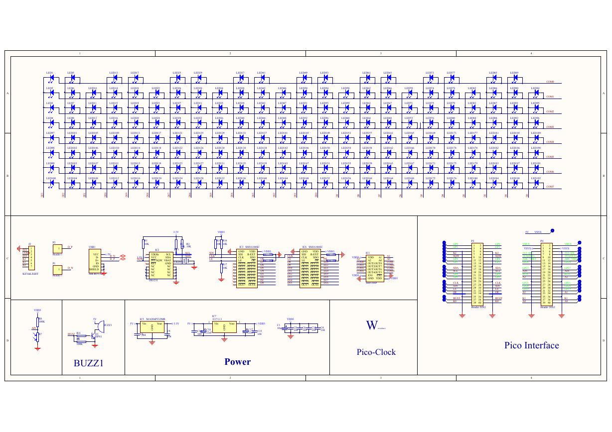 原理图(Pico-Clock-Green-Schdoc).pdf
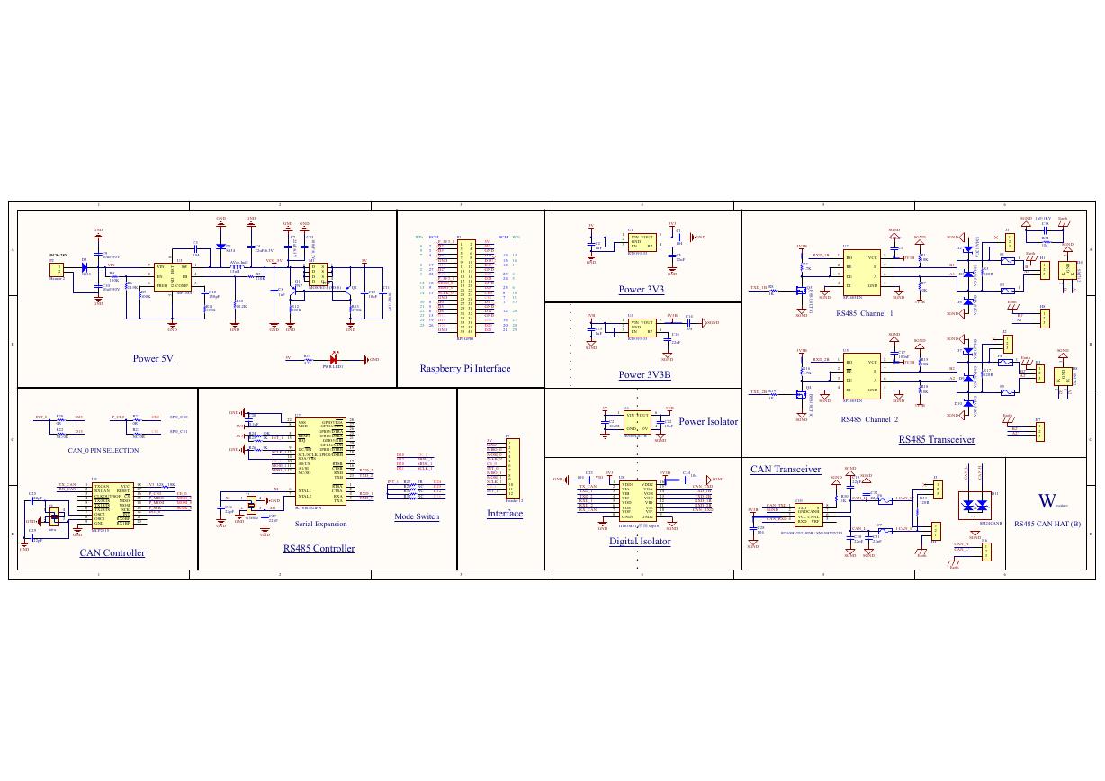 原理图(RS485-CAN-HAT-B-schematic).pdf
 File:SIM7500_SIM7600_SIM7800 Series_SSL_Application Note_V2.00.pdf
 ADS1263(Ads1262).pdf
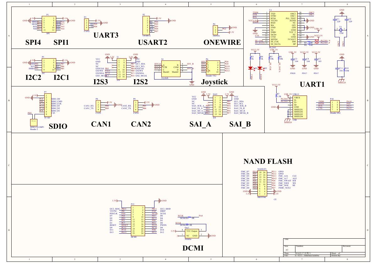 原理图(Open429Z-D-Schematic).pdf
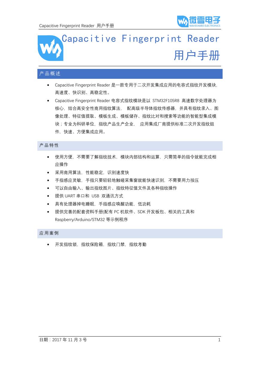 用户手册(Capacitive_Fingerprint_Reader_User_Manual_CN).pdf
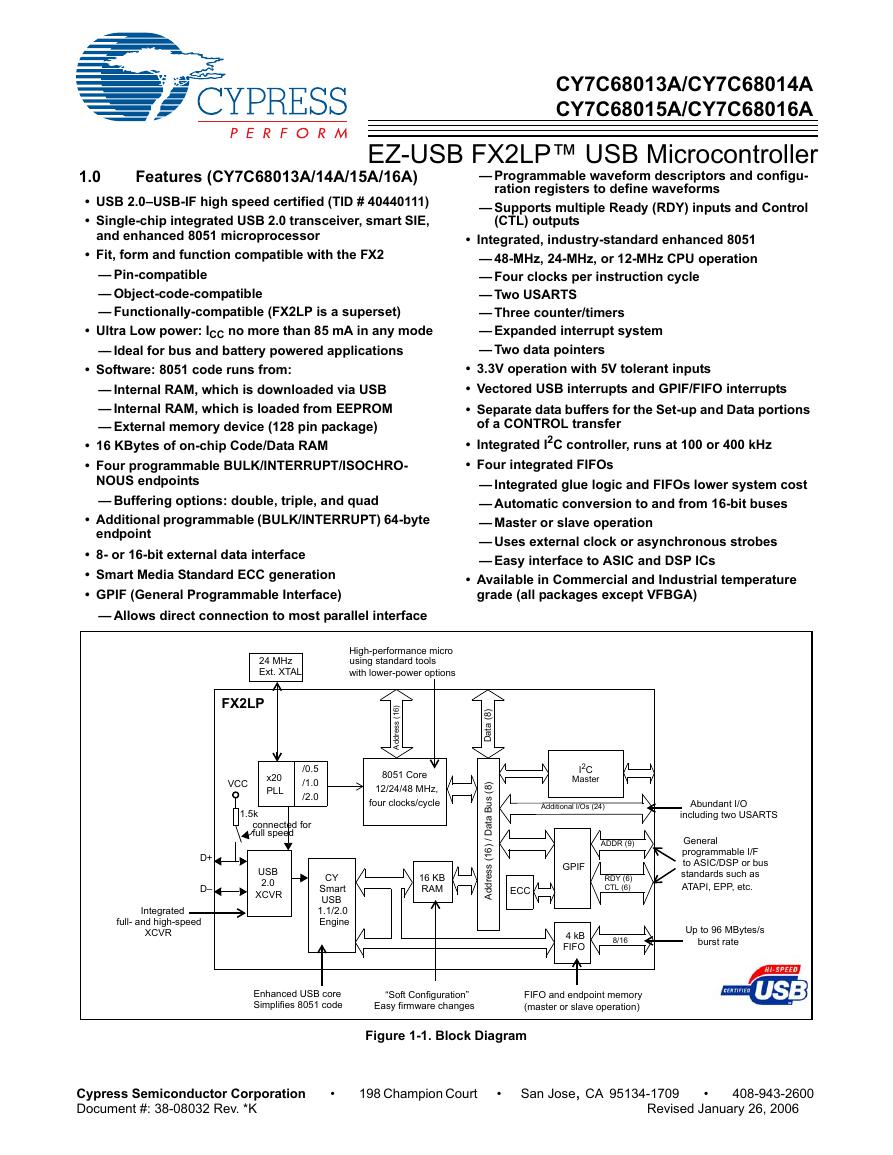 CY7C68013A(英文版)(CY7C68013A).pdf
 TechnicalReference_Dem.pdf