Version: 1.0
Technical Specification
MODEL NO: 7.3inch e-Paper (F)
The content of this information is subject to be changed without
notice. Please contact Waveshare
7.3inch e-Paper (F)�
Revision History
Rev.
Issued Date
Revised Contents
0.1
1.0
2021.09.10
2021.11.29
Tentative
Final
7.3inch e-Paper (F)�
TECHNICAL SPECIFICATION
CONTENTS
1. Application ..................................................................................................................................................... 1
2. Features .......................................................................................................................................................... 1
3. Mechanical Specifications .............................................................................................................................. 1
4. Mechanical Drawing of EPD Module .............................................................................................................. 2
5.
Input/Output Interface ..................................................................................................................................... 3
6. Command Table ............................................................................................................................................. 6
7. Electrical Characteristics ................................................................................................................................. 8
8. Optical Characteristics .................................................................................................................................. 16
9. Handling, Safety and Environmental Requirements and Remark ................................................................... 17
10. Reliability Test ............................................................................................................................................. 19
11. Block Diagram ............................................................................................................................................. 20
7.3inch e-Paper (F)�
1. Application
This is a reflective electrophoretic E Ink® technology display module on an active matrix TFT substrate.
The diagonal length of the active area is 7.3” and contains 800 x 480 pixels. The panel is capable of displaying
7-colors of black, white, red, yellow, blue, green, and orange images depending on the associated lookup table
used. The circuitry on the panel includes an integrated gate and source driver, timing controller, oscillator, DC-
DC boost circuit, and memory to store the frame buffer and lookup tables, and additional circuitry to control
VCOM and BORDER settings.
2.
Features
E Ink Gallery Palette™ display
High contrast TFT electrophoretic
800 x 480 display
High reflectance
Ultra wide viewing angle
Ultra low power consumption
Pure reflective mode
Bi-stable
Low current sleep mode
On chip display RAM
Serial Peripheral Interface
External SPI flash/eeprom for waveform
On-chip oscillator
On-chip booster and regulator control for generating Vcom, Gate and Source driving voltage
I2C Signal Master Interface to read external temperature sensor
Operational temperature range (15 ~ 35℃)
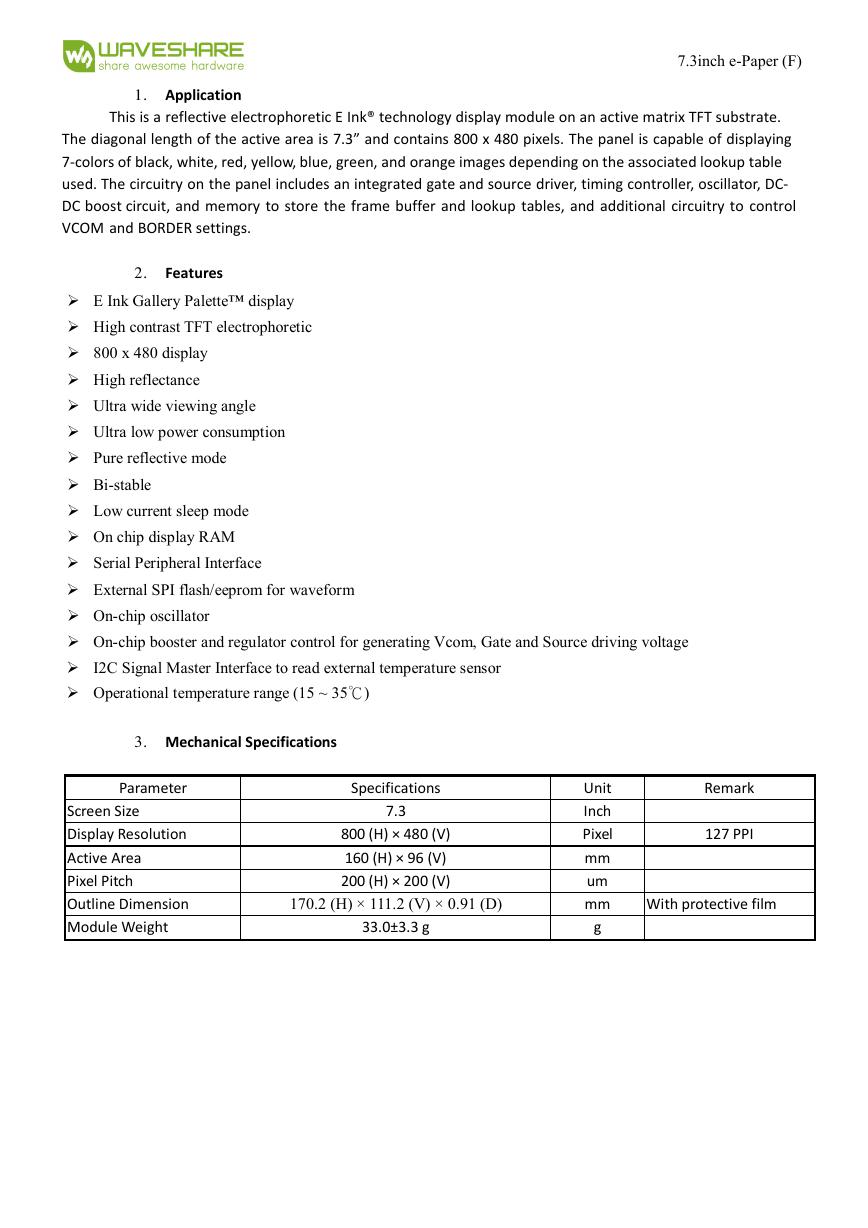
3. Mechanical Specifications
Parameter
Screen Size
Display Resolution
Active Area
Pixel Pitch
Outline Dimension
Module Weight
Specifications
7.3
800 (H) × 480 (V)
160 (H) × 96 (V)
200 (H) × 200 (V)
170.2 (H) × 111.2 (V) × 0.91 (D)
33.0±3.3 g
Remark
127 PPI
With protective film
Unit
Inch
Pixel
mm
um
mm
g
7.3inch e-Paper (F)�
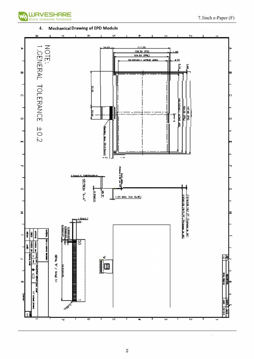
4.
Mechanical
Drawing
of EPD Module
_....._
9)
_!,.11_
主
竺
卜
-i
'|
'|
'|
'
l-__
-_
4'|
'|
'|
'
i
i
i
�
|
l
'|
'
T
A
i
i
'|__
1今20UAX.(W亟
N
O
T
E
:
1
.G
E
N
E
R
A
L
T
O
L
E
R
A
N
C
E
片
0
.2
王
。
。
。
m
..,
。
::c
c...
`
li
a
F
d
.
、
只
丘
5
�
1
►
口
。
。
m
..,
。
::c
;;
�le..
.
i
g玉
,
0
.9
1怜
0
.
8
(
W、P
F.
Th
iel
5
8
·
亨
仁b}
o.s
5
1:
.09
o
r
w、o
P
F'
,
Th
i
e
亏
$
”
了
仁b
4
。
。
忐偷
L
卜
o
!
父
1
黛=
g
-
L
.
7.3inch e-Paper (F)�
5.
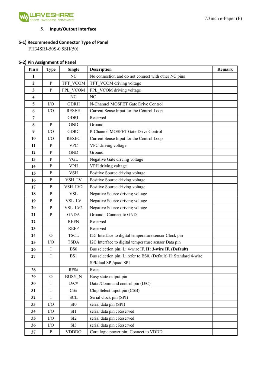
Input/Output Interface
5-1) Recommended Connector Type of Panel
FH34SRJ-50S-0.5SH(50)
5-2) Pin Assignment of Panel
Pin #
Type
Single
Description
Remark
1
2
3
4
5
6
7
8
9
10
11
12
13
14
15
16
17
18
19
20
21
22
23
24
25
26
27
28
29
30
31
32
33
34
35
36
37
P
P
I/O
I/O
P
I/O
I/O
P
P
P
P
P
P
P
P
P
P
P
O
I/O
I
I
I
O
I
I
I
I/O
I/O
I/O
I/O
P
NC
No connection and do not connect with other NC pins
TFT_VCOM TFT_VCOM driving voltage
FPL_VCOM FPL_VCOM driving voltage
NC
NC
GDRH
N-Channel MOSFET Gate Drive Control
RESEH
Current Sense Input for the Control Loop
GDRL
Reserved
GND
Ground
GDRC
P-Channel MOSFET Gate Drive Control
RESEC
Current Sense Input for the Control Loop
VPC
GND
VGL
VPH
VSH
VPC driving voltage
Ground
Negative Gate driving voltage
VPH driving voltage
Positive Source driving voltage
VSH_LV
Positive Source driving voltage
VSH_LV2
Positive Source driving voltage
VSL
Negative Source driving voltage
VSL_LV
Negative Source driving voltage
VSL_LV2 Negative Source driving voltage
GNDA
Ground ; Connect to GND
REFN
Reserved
REFP
TSCL
Reserved
I2C Interface to digital temperature sensor Clock pin
TSDA
I2C Interface to digital temperature sensor Data pin
BS0
BS1
Bus selection pin; L: 4-wire IF. H: 3-wire IF. (Default)
Bus selection pin; L: refer to BS0. (Default) H: Standard 4-wire
SPI/dual SPI/quad SPI
RES#
Reset
BUSY_N
Busy state output pin
D/C#
CS#
SCL
SI0
SI1
SI2
SI3
Data /Command control pin (D/C)
Chip Select input pin (CSB)
Serial clock pin (SPI)
serial data pin (SPI)
serial data pin ; Reserved
serial data pin ; Reserved
serial data pin ; Reserved
VDDDO
Core logic power pin; Connect to VDDD
7.3inch e-Paper (F)�
38
39
40
41
42
43
44
45
46
47
48
49
50
P
P
P
P
P
P
P
P
P
P
P
VDD
GND
Supply voltage
Ground; Connect to GNDA
VDDIO
Supply voltage
VCP2
CP2N
CP2P
VCP1
CP1N
CP1P
Charge Pump Pin
Charge Pump Pin
Charge Pump Pin
Charge Pump Pin
Charge Pump Pin
Charge Pump Pin
CGH1N
Charge Pump Pin; Reserved
CGH1P
Charge Pump Pin; Reserved
VGH
Positive Gate driving voltage
VCOMBD VCOMBD driving voltage
Note 5-1: This pin (CS#) is the chip select input connecting to the MCU. The chip is enabled for MCU communication only when CS# is
pulled Low.
Note 5-2: This pin (D/C#) is Data/Command control pin connecting to the MCU. When the pin is pulled HIGH, the data will be interpreted
as data. When the pin is pulled Low, the data will be interpreted as command.
Note 5-3: This pin (RES#) is reset signal input. The Reset is active Low.
Note 5-4: This pin (BUSY_N) is Busy state output pin. When Busy is low, the operation of chip should not be interrupted and any
commands should not be issued to the module. The driver IC will put Busy pin low when the driver IC is working such as:
- Outputting display waveform; or
- Programming with OTP
- Communicating with digital temperature sensor
Note 5-5: This pin (BS0) is for 3-line SPI or 4-line SPI selection. When it is “Low”, 4-line SPI is selected. When it is “High”, 3-line SPI (9
bits SPI) is selected. Please refer to below Table.
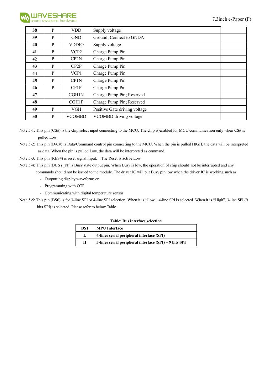
Table: Bus interface selection
BS1 MPU Interface
L
H
4-lines serial peripheral interface (SPI)
3-lines serial peripheral interface (SPI) – 9 bits SPI
7.3inch e-Paper (F)�
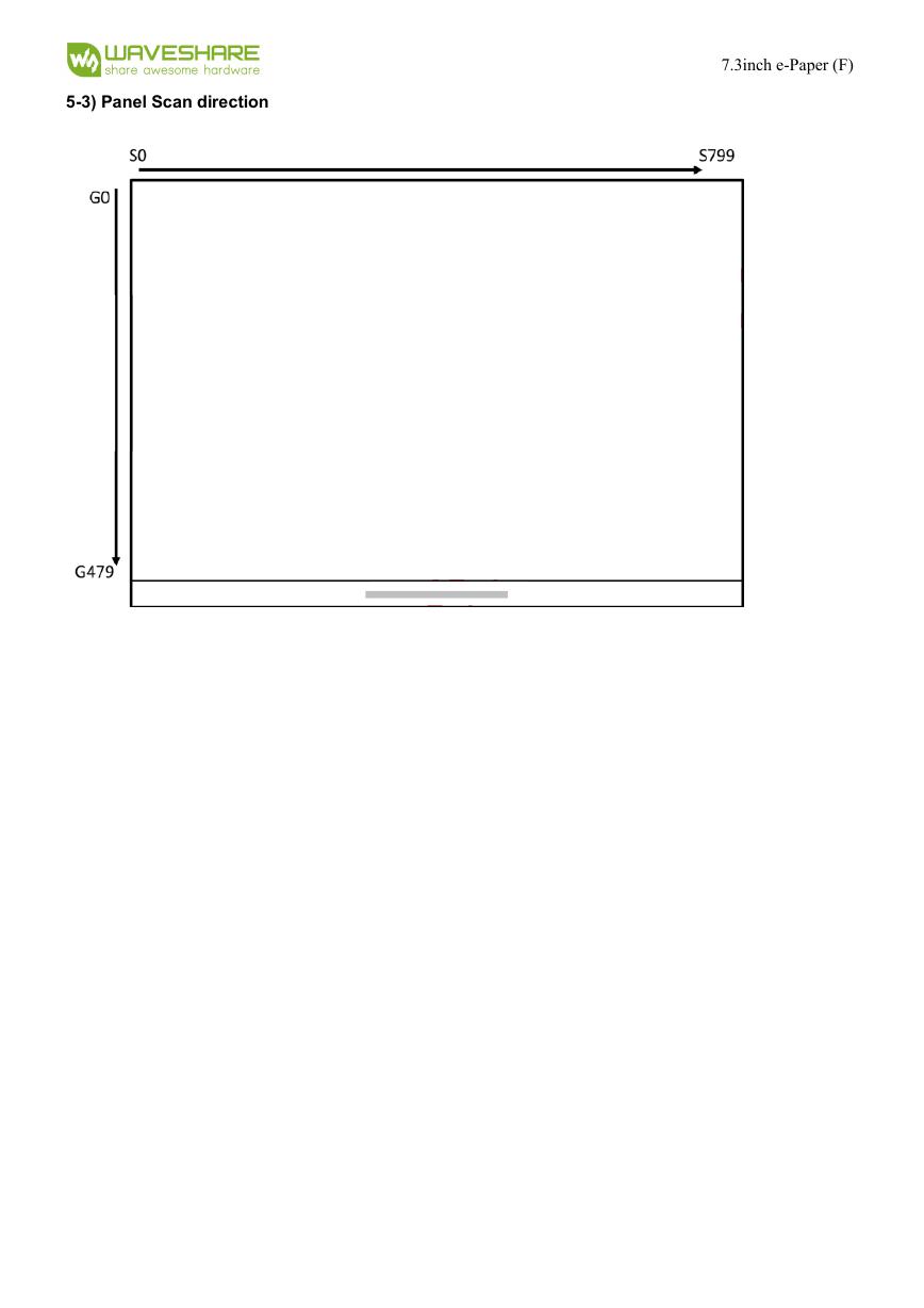
5-3) Panel Scan direction
7.3inch e-Paper (F)�



 V2版本原理图(Capacitive-Fingerprint-Reader-Schematic_V2).pdf
 摄像头工作原理.doc
 VL53L0X简要说明(En.FLVL53L00216).pdf
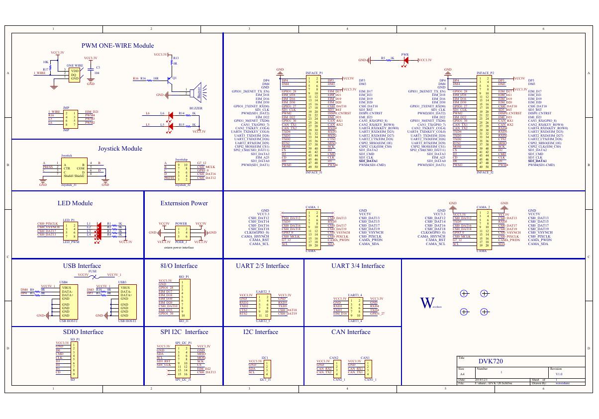 原理图(DVK720-Schematic).pdf
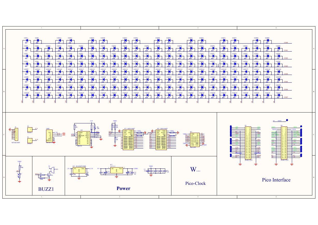 原理图(Pico-Clock-Green-Schdoc).pdf
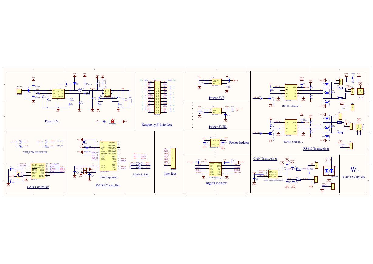 原理图(RS485-CAN-HAT-B-schematic).pdf
 File:SIM7500_SIM7600_SIM7800 Series_SSL_Application Note_V2.00.pdf
 ADS1263(Ads1262).pdf
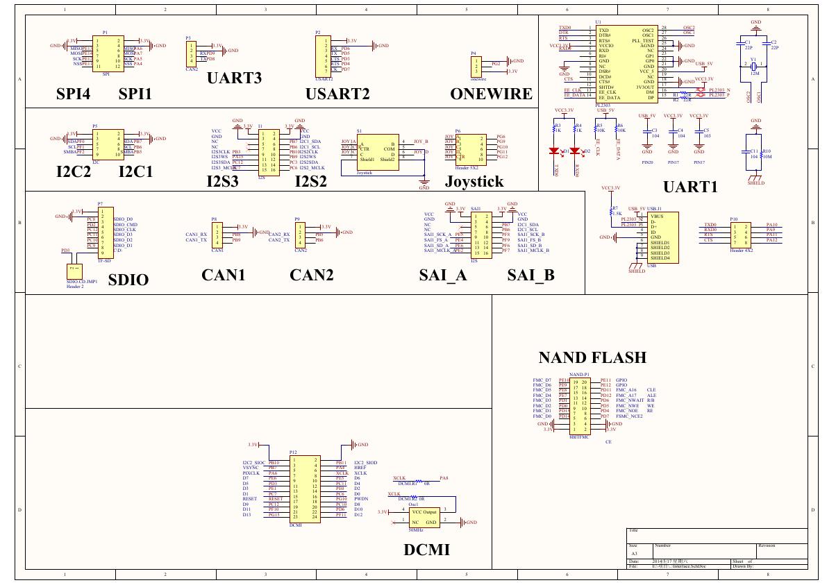 原理图(Open429Z-D-Schematic).pdf
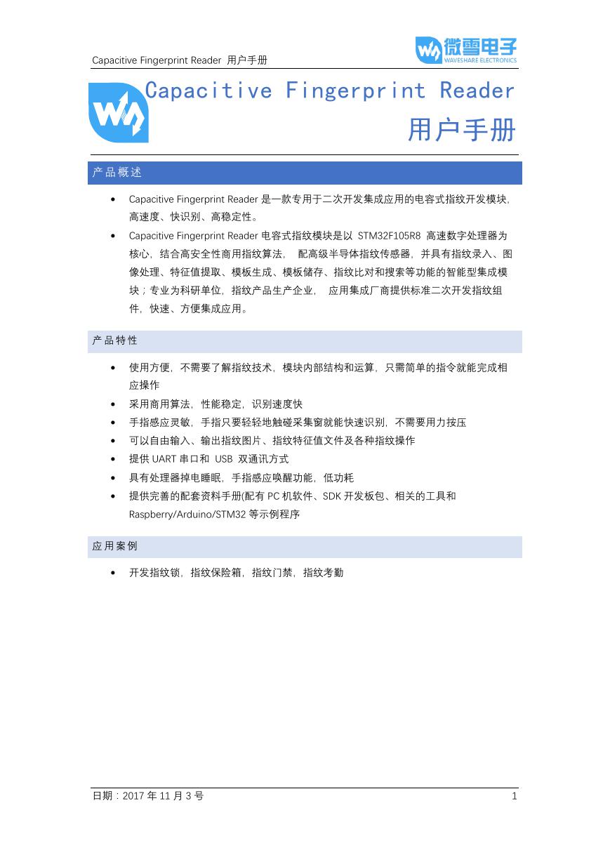 用户手册(Capacitive_Fingerprint_Reader_User_Manual_CN).pdf
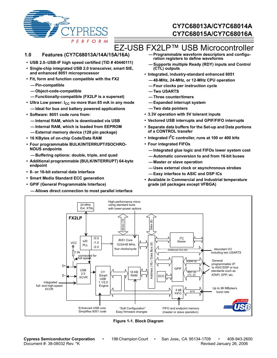 CY7C68013A(英文版)(CY7C68013A).pdf
 TechnicalReference_Dem.pdf