PCF8563
Real-time clock/calendar
Rev. 06 — 21 February 2008
Product data sheet
1. General description
2. Features
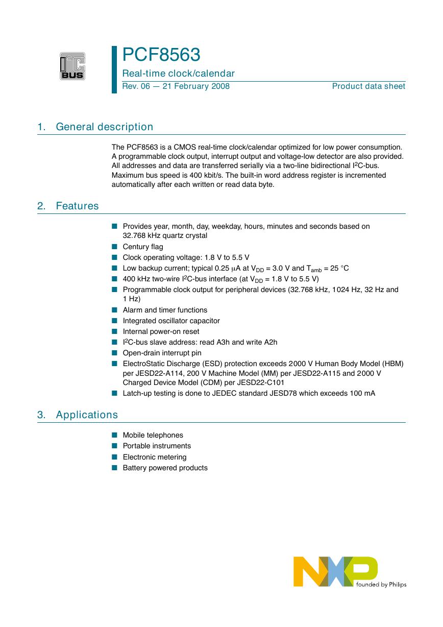
The PCF8563 is a CMOS real-time clock/calendar optimized for low power consumption.
A programmable clock output, interrupt output and voltage-low detector are also provided.
All addresses and data are transferred serially via a two-line bidirectional I2C-bus.
Maximum bus speed is 400 kbit/s. The built-in word address register is incremented
automatically after each written or read data byte.
n Provides year, month, day, weekday, hours, minutes and seconds based on
32.768 kHz quartz crystal
n Century flag
n Clock operating voltage: 1.8 V to 5.5 V
n Low backup current; typical 0.25 m A at VDD = 3.0 V and Tamb = 25 C
n 400 kHz two-wire I2C-bus interface (at VDD = 1.8 V to 5.5 V)
n Programmable clock output for peripheral devices (32.768 kHz, 1024 Hz, 32 Hz and
1 Hz)
n Alarm and timer functions
n Integrated oscillator capacitor
n Internal power-on reset
n I2C-bus slave address: read A3h and write A2h
n Open-drain interrupt pin
n ElectroStatic Discharge (ESD) protection exceeds 2000 V Human Body Model (HBM)
per JESD22-A114, 200 V Machine Model (MM) per JESD22-A115 and 2000 V
Charged Device Model (CDM) per JESD22-C101
n Latch-up testing is done to JEDEC standard JESD78 which exceeds 100 mA
3. Applications
n Mobile telephones
n Portable instruments
n Electronic metering
n Battery powered products
�
NXP Semiconductors
4. Ordering information
PCF8563
Real-time clock/calendar
Table 1.
Type number Topside
Ordering information
mark
PCF8563P
PCF8563T
PCF8563TS
PCF8563P
8563T
8563
Package
Name
DIP8
SO8
TSSOP8
PCF8563BS
8563S
HVSON10
5. Block diagram
Description
plastic dual in-line package; 8 leads (300 mil)
plastic small outline package; 8 leads; body width 3.9 mm
plastic thin shrink small outline package; 8 leads; body width
3 mm
plastic thermal enhanced very thin small outline package;
no leads; 10 terminals; body 3 · 3 · 0.85 mm
Version
SOT97-1
SOT96-1
SOT505-1
SOT650-1
OSCILLATOR
32.768 kHz
DIVIDER
CLOCK OUT
CLKOUT
CONTROL
CONTROL_STATUS_1
CONTROL_STATUS_2
CLKOUT_CONTROL
TIME
VL_SECONDS
MINUTES
HOURS
DAYS
WEEKDAYS
CENTURY_MONTHS
YEARS
ALARM FUNCTION
MINUTE_ALARM
HOUR_ALARM
DAY_ALARM
WEEKDAY_ALARM
TIMER FUNCTION
TIMER_CONTROL
TIMER
00
01
0D
02
03
04
05
06
07
08
09
0A
0B
0C
0E
0F
INTERRUPT
INT
001aah658
OSCI
OSCO
VDD
VSS
MONITOR
POWER ON
RESET
WATCH
DOG
SDA
SCL
I2C-BUS
INTERFACE
PCF8563
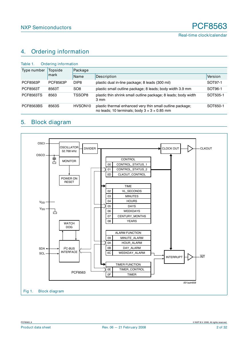
Fig 1. Block diagram
PCF8563_6
Product data sheet
Rev. 06 — 21 February 2008
© NXP B.V. 2008. All rights reserved.
2 of 32
�
NXP Semiconductors
6. Pinning information
6.1 Pinning
PCF8563
Real-time clock/calendar
OSCI
OSCO
INT
VSS
1
2
3
4
PCF8563P
8
7
6
5
VDD
CLKOUT
SCL
SDA
OSCI
OSCO
INT
VSS
1
2
3
4
PCF8563T
8
7
6
5
VDD
CLKOUT
SCL
SDA
001aaf977
001aaf975
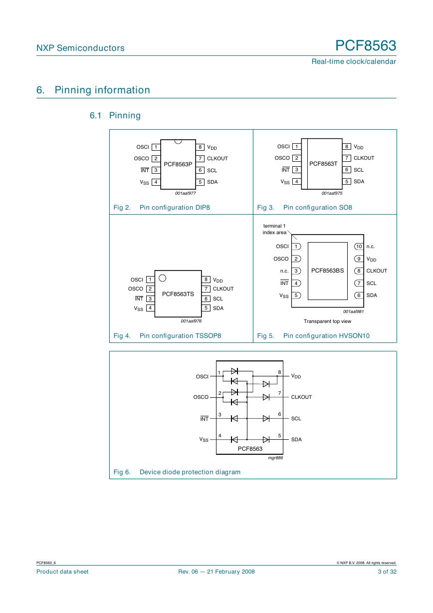
Fig 2.
Pin configuration DIP8
Fig 3.
Pin configuration SO8
terminal 1
index area
OSCI
OSCO
n.c.
INT
VSS
1
2
3
4
5
PCF8563BS
10
n.c.
9
8
7
6
VDD
CLKOUT
SCL
SDA
001aaf981
Transparent top view
OSCI
OSCO
INT
VSS
1
2
3
4
8
7
6
5
VDD
CLKOUT
SCL
SDA
PCF8563TS
001aaf976
Fig 4.
Pin configuration TSSOP8
Fig 5.
Pin configuration HVSON10
OSCI
OSCO
INT
VSS
1
2
3
4
8
7
6
5
VDD
CLKOUT
SCL
SDA
Fig 6. Device diode protection diagram
PCF8563
mgr886
PCF8563_6
Product data sheet
Rev. 06 — 21 February 2008
© NXP B.V. 2008. All rights reserved.
3 of 32
�
NXP Semiconductors
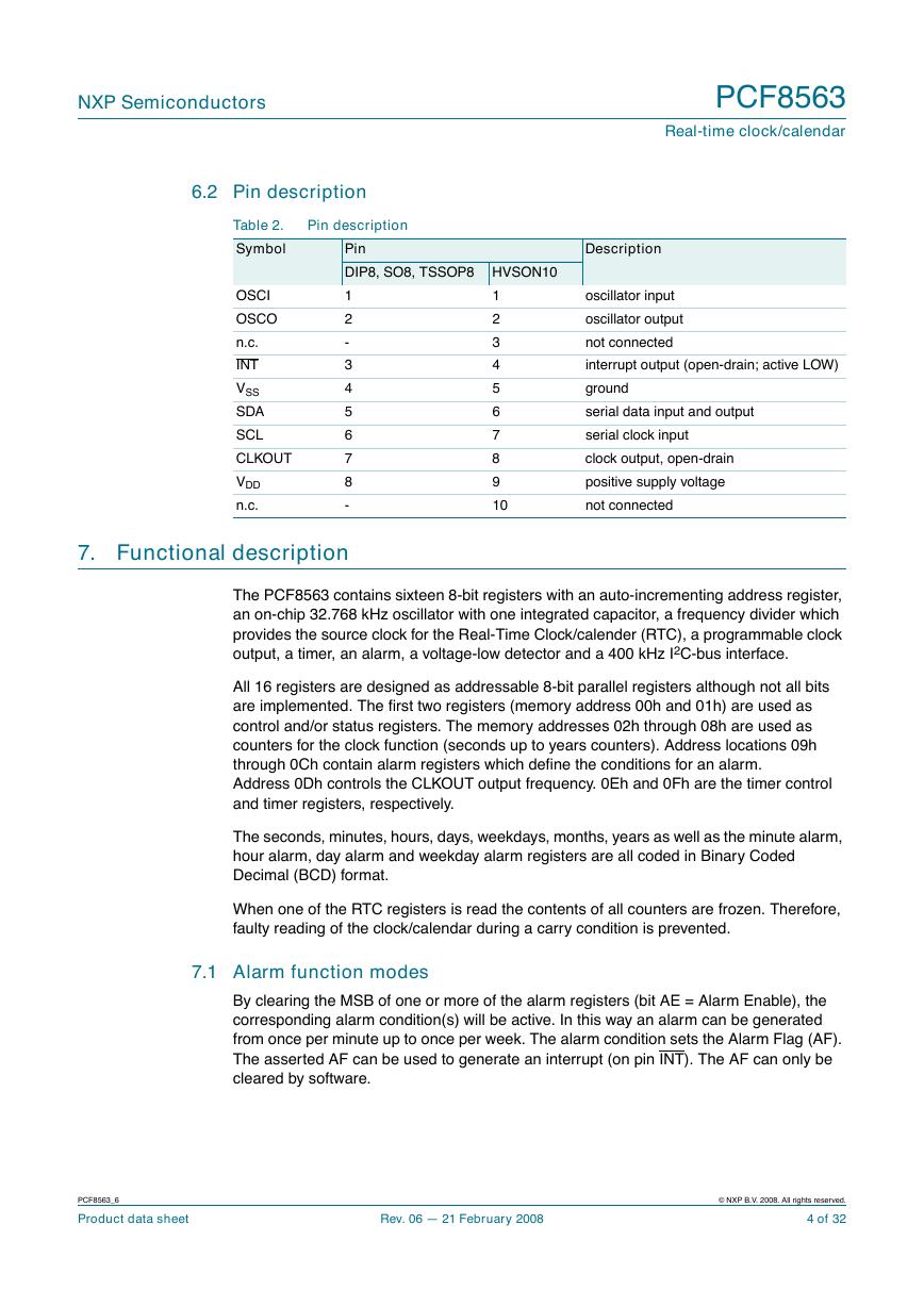
6.2 Pin description
PCF8563
Real-time clock/calendar
Table 2.
Symbol
OSCI
OSCO
n.c.
INT
VSS
SDA
SCL
CLKOUT
VDD
n.c.
Pin description
Pin
DIP8, SO8, TSSOP8 HVSON10
1
2
-
3
4
5
6
7
8
-
1
2
3
4
5
6
7
8
9
10
Description
oscillator input
oscillator output
not connected
interrupt output (open-drain; active LOW)
ground
serial data input and output
serial clock input
clock output, open-drain
positive supply voltage
not connected
7. Functional description
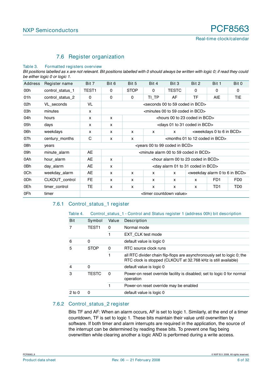
The PCF8563 contains sixteen 8-bit registers with an auto-incrementing address register,
an on-chip 32.768 kHz oscillator with one integrated capacitor, a frequency divider which
provides the source clock for the Real-Time Clock/calender (RTC), a programmable clock
output, a timer, an alarm, a voltage-low detector and a 400 kHz I2C-bus interface.
All 16 registers are designed as addressable 8-bit parallel registers although not all bits
are implemented. The first two registers (memory address 00h and 01h) are used as
control and/or status registers. The memory addresses 02h through 08h are used as
counters for the clock function (seconds up to years counters). Address locations 09h
through 0Ch contain alarm registers which define the conditions for an alarm.
Address 0Dh controls the CLKOUT output frequency. 0Eh and 0Fh are the timer control
and timer registers, respectively.
The seconds, minutes, hours, days, weekdays, months, years as well as the minute alarm,
hour alarm, day alarm and weekday alarm registers are all coded in Binary Coded
Decimal (BCD) format.
When one of the RTC registers is read the contents of all counters are frozen. Therefore,
faulty reading of the clock/calendar during a carry condition is prevented.
7.1 Alarm function modes
By clearing the MSB of one or more of the alarm registers (bit AE = Alarm Enable), the
corresponding alarm condition(s) will be active. In this way an alarm can be generated
from once per minute up to once per week. The alarm condition sets the Alarm Flag (AF).
The asserted AF can be used to generate an interrupt (on pin INT). The AF can only be
cleared by software.
PCF8563_6
Product data sheet
Rev. 06 — 21 February 2008
© NXP B.V. 2008. All rights reserved.
4 of 32
�
NXP Semiconductors
7.2 Timer
PCF8563
Real-time clock/calendar
The 8-bit countdown timer at address 0Fh is controlled by the timer control register at
address 0Eh. The timer control register determines one of 4 source clock frequencies for
the timer (4096 Hz, 64 Hz, 1 Hz, or 1⁄60 Hz), and enables or disables the timer. The timer
counts down from a software-loaded 8-bit binary value. At the end of every countdown,
the timer sets the Timer Flag (TF). The TF may only be cleared by software. The
asserted TF can be used to generate an interrupt (on pin INT). The interrupt may be
generated as a pulsed signal every countdown period or as a permanently active signal
which follows the state of TF. Bit TI_TP is used to control this mode selection. When
reading the timer, the current countdown value is returned.
7.3 Clock output
A programmable square wave is available at pin CLKOUT. Operation is controlled by the
CLKOUT control register at address 0Dh. Frequencies of 32.768 kHz (default), 1024 Hz,
32 Hz and 1 Hz can be generated for use as a system clock, microcontroller clock, input to
a charge pump, or for calibration of the oscillator. CLKOUT is an open-drain output and
enabled at power-on. If disabled it becomes high-impedance.
7.4 Reset
The PCF8563 includes an internal reset circuit which is active whenever the oscillator is
stopped. In the reset state the I2C-bus logic is initialized and all registers are reset
according to Table 25.
7.5 Voltage-low detector
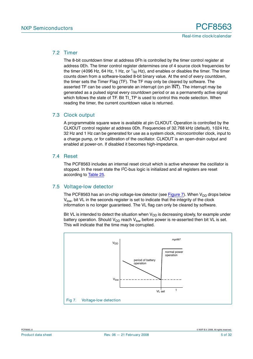
The PCF8563 has an on-chip voltage-low detector (see Figure 7). When VDD drops below
Vlow, bit VL in the seconds register is set to indicate that the integrity of the clock
information is no longer guaranteed. The VL flag can only be cleared by software.
Bit VL is intended to detect the situation when VDD is decreasing slowly, for example under
battery operation. Should VDD reach Vlow before power is re-asserted then bit VL is set.
This will indicate that the time may be corrupted.
mgr887
normal power
operation
period of battery
operation
VDD
Vlow
Fig 7.
Voltage-low detection
VL set
t
PCF8563_6
Product data sheet
Rev. 06 — 21 February 2008
© NXP B.V. 2008. All rights reserved.
5 of 32
�
NXP Semiconductors
7.6 Register organization
PCF8563
Real-time clock/calendar
Bit 2
0
TF
Bit 1
0
AIE
Bit 0
0
TIE
Bit 5
STOP
0
Bit 7
TEST1
Bit 6
Bit 4
0
TI_TP
Bit 3
TESTC
AF
0
VL
x
x
x
x
C
Formatted registers overview
Table 3.
Bitpositionslabelledasxarenotrelevant.Bitpositionslabelledwith0shouldalwaysbewrittenwithlogic0;ifreadtheycould
be either logic0 or logic1.
Address Register name
control_status_1
00h
control_status_2
01h
02h
VL_seconds
minutes
03h
hours
04h
05h
days
weekdays
06h
century_months
07h
years
08h
09h
minute_alarm
hour_alarm
0Ah
day_alarm
0Bh
0Ch
weekday_alarm
CLKOUT_control
0Dh
timer_control
0Eh
0Fh
timer
x
x
x
0
0
x
x
x
x
x
x
x
x
x
AE
AE
AE
AE
FE
TE
FD1
TD1
FD0
TD0
x
x
x
x
x
x
x
x
x
x
x
x
7.6.1 Control_status_1 register
Control_status_1 - Control and Status register 1 (address 00h) bit description
Table 4.
Bit
7
6
5
4
3
Symbol
TEST1
0
STOP
0
TESTC
2 to 0
0
0
1
Value Description
Normal mode
0
EXT_CLK test mode
1
default value is logic 0
RTC source clock runs
all RTC divider chain flip-flops are asynchronously set to logic 0; the
RTC clock is stopped (CLKOUT at 32.768 kHz is still available)
default value is logic 0
Power-on reset override facility is disabled; set to logic 0 for normal
operation
Power-on reset override may be enabled
default value is logic 0
0
1
7.6.2 Control_status_2 register
Bits TF and AF: When an alarm occurs, AF is set to logic 1. Similarly, at the end of a timer
countdown, TF is set to logic 1. These bits maintain their value until overwritten by
software. If both timer and alarm interrupts are required in the application, the source of
the interrupt can be determined by reading these bits. To prevent one flag being
overwritten while clearing another a logic AND is performed during a write access.
PCF8563_6
Product data sheet
Rev. 06 — 21 February 2008
© NXP B.V. 2008. All rights reserved.
6 of 32
�
NXP Semiconductors
PCF8563
Real-time clock/calendar
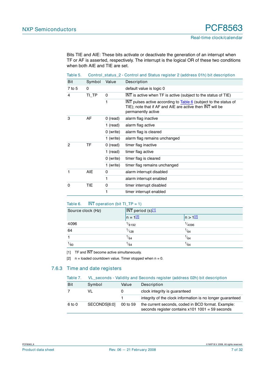
Bits TIE and AIE: These bits activate or deactivate the generation of an interrupt when
TF or AF is asserted, respectively. The interrupt is the logical OR of these two conditions
when both AIE and TIE are set.
Control_status_2 - Control and Status register 2 (address 01h) bit description
Symbol Value
0
TI_TP
Description
default value is logic 0
INT is active when TF is active (subject to the status of TIE)
INT pulses active according to Table 6 (subject to the status of
TIE); note that if AF and AIE are active then INT will be
permanently active
alarm flag inactive
alarm flag active
alarm flag is cleared
alarm flag remains unchanged
timer flag inactive
timer flag active
timer flag is cleared
timer flag remains unchanged
alarm interrupt disabled
alarm interrupt enabled
timer interrupt disabled
timer interrupt enabled
0
1
AF
TF
AIE
TIE
0 (read)
1 (read)
0 (write)
1 (write)
0 (read)
1 (read)
0 (write)
1 (write)
0
1
0
1
Table 6.
Source clock (Hz)
INT operation (bit TI_TP = 1)
INT period (s)[1]
n = 1[2]
1⁄8192
1⁄128
1⁄64
1⁄64
n > 1[2]
1⁄4096
1⁄64
1⁄64
1⁄64
Table 5.
Bit
7 to 5
4
3
2
1
0
4096
64
1
1⁄60
Table 7.
Bit
7
[1] TF and INT become active simultaneously.
[2]
n = loaded countdown value. Timer stopped when n = 0.
7.6.3 Time and date registers
VL_seconds - Validity and Seconds register (address 02h) bit description
Symbol
VL
Description
clock integrity is guaranteed
integrity of the clock information is no longer guaranteed
the current seconds, coded in BCD format. Example:
seconds register contains x101 1001 = 59 seconds
Value
0
1
00 to 59
6 to 0
SECONDS[6:0]
PCF8563_6
Product data sheet
Rev. 06 — 21 February 2008
© NXP B.V. 2008. All rights reserved.
7 of 32
�
NXP Semiconductors
PCF8563
Real-time clock/calendar
Table 8.
Bit
7
6 to 0
Table 9.
Bit
7 to 6
5 to 0
Minutes - Minutes register (address 03h) bit description
Symbol
x
MINUTES[6:0]
Description
not relevant
the current minutes, coded in BCD format
00 to 59
Value
Hours - Hours register (address 04h) bit description
Symbol
x
HOURS[5:0]
Description
not relevant
the current hours, coded in BCD format
00 to 23
Value
Table 10. Days - Days register (address 05h) bit description
Bit
7 to 6
5 to 0
Description
not relevant
the current day, coded in BCD format[1]
Symbol
x
DAYS[5:0]
01 to 31
Value
[1] The PCF8563 compensates for leap years by adding a 29th day to February if the year counter contains a
value which is exactly divisible by 4, including the year 00.
Table 11. Weekdays - Weekdays register (address 06h) bit description
Bit
7 to 3
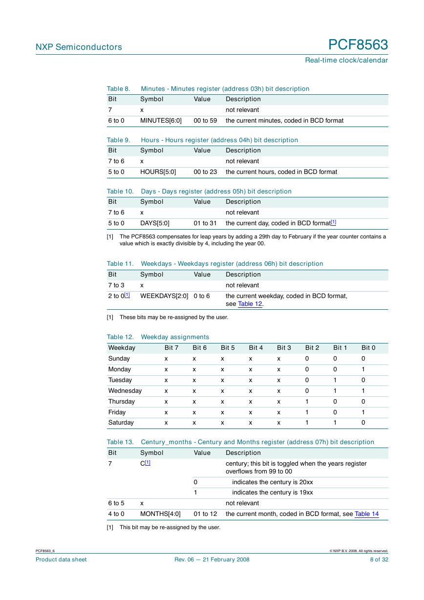
2 to 0[1] WEEKDAYS[2:0] 0 to 6
Description
not relevant
the current weekday, coded in BCD format,
see Table 12.
Symbol
x
Value
[1] These bits may be re-assigned by the user.
Table 12. Weekday assignments
Bit 6
Weekday
x
Sunday
x
Monday
Tuesday
x
x
Wednesday
x
Thursday
Friday
x
x
Saturday
Bit 7
x
x
x
x
x
x
x
Bit 5
x
x
x
x
x
x
x
Bit 4
x
x
x
x
x
x
x
Bit 3
x
x
x
x
x
x
x
Bit 2
0
0
0
0
1
1
1
Bit 1
0
0
1
1
0
0
1
Bit 0
0
1
0
1
0
1
0
Table 13. Century_months - Century and Months register (address 07h) bit description
Bit
7
Description
century; this bit is toggled when the years register
overflows from 99 to 00
Symbol
C[1]
Value
0
1
indicates the century is 20xx
indicates the century is 19xx
6 to 5
4 to 0
x
MONTHS[4:0]
not relevant
the current month, coded in BCD format, see Table 14
01 to 12
[1] This bit may be re-assigned by the user.
PCF8563_6
Product data sheet
Rev. 06 — 21 February 2008
© NXP B.V. 2008. All rights reserved.
8 of 32
�


 V2版本原理图(Capacitive-Fingerprint-Reader-Schematic_V2).pdf
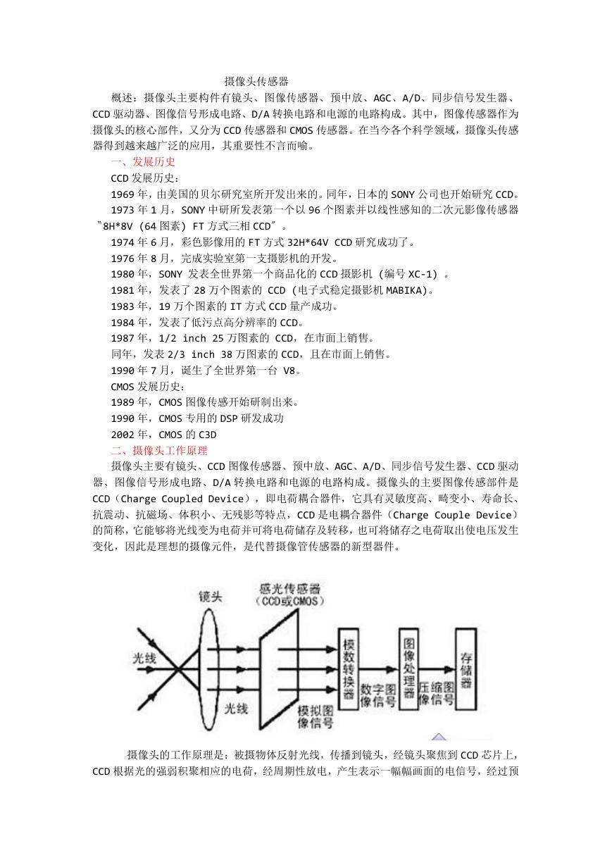 摄像头工作原理.doc
 VL53L0X简要说明(En.FLVL53L00216).pdf
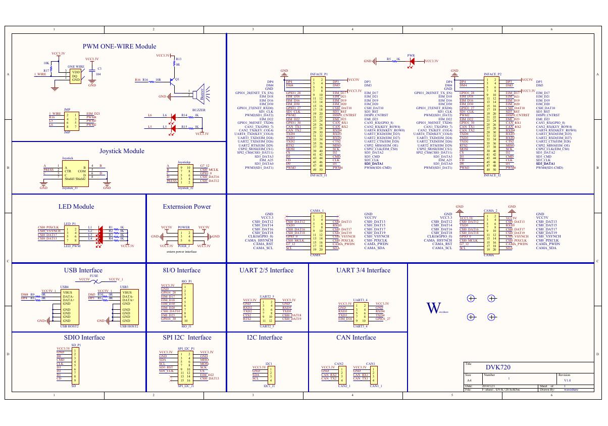 原理图(DVK720-Schematic).pdf
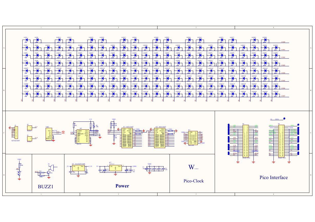 原理图(Pico-Clock-Green-Schdoc).pdf
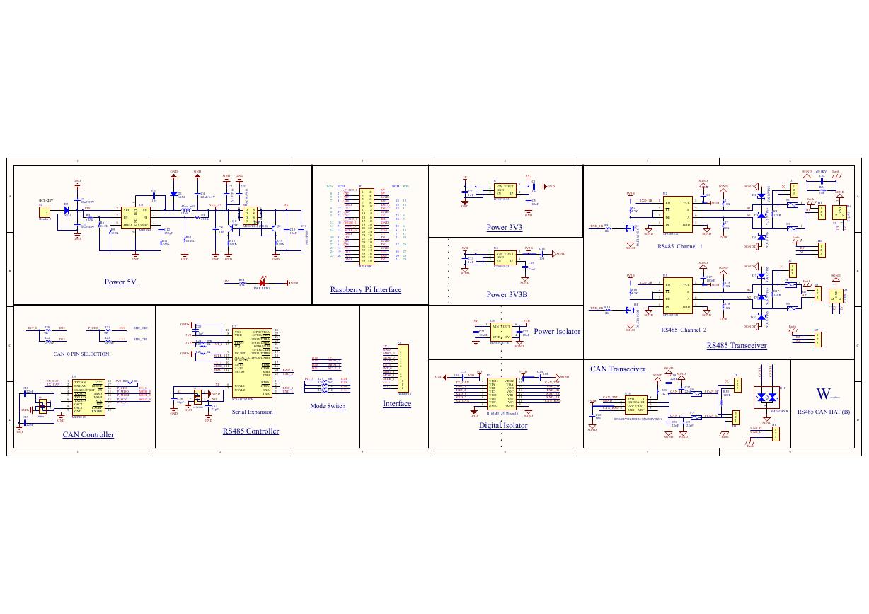 原理图(RS485-CAN-HAT-B-schematic).pdf
 File:SIM7500_SIM7600_SIM7800 Series_SSL_Application Note_V2.00.pdf
 ADS1263(Ads1262).pdf
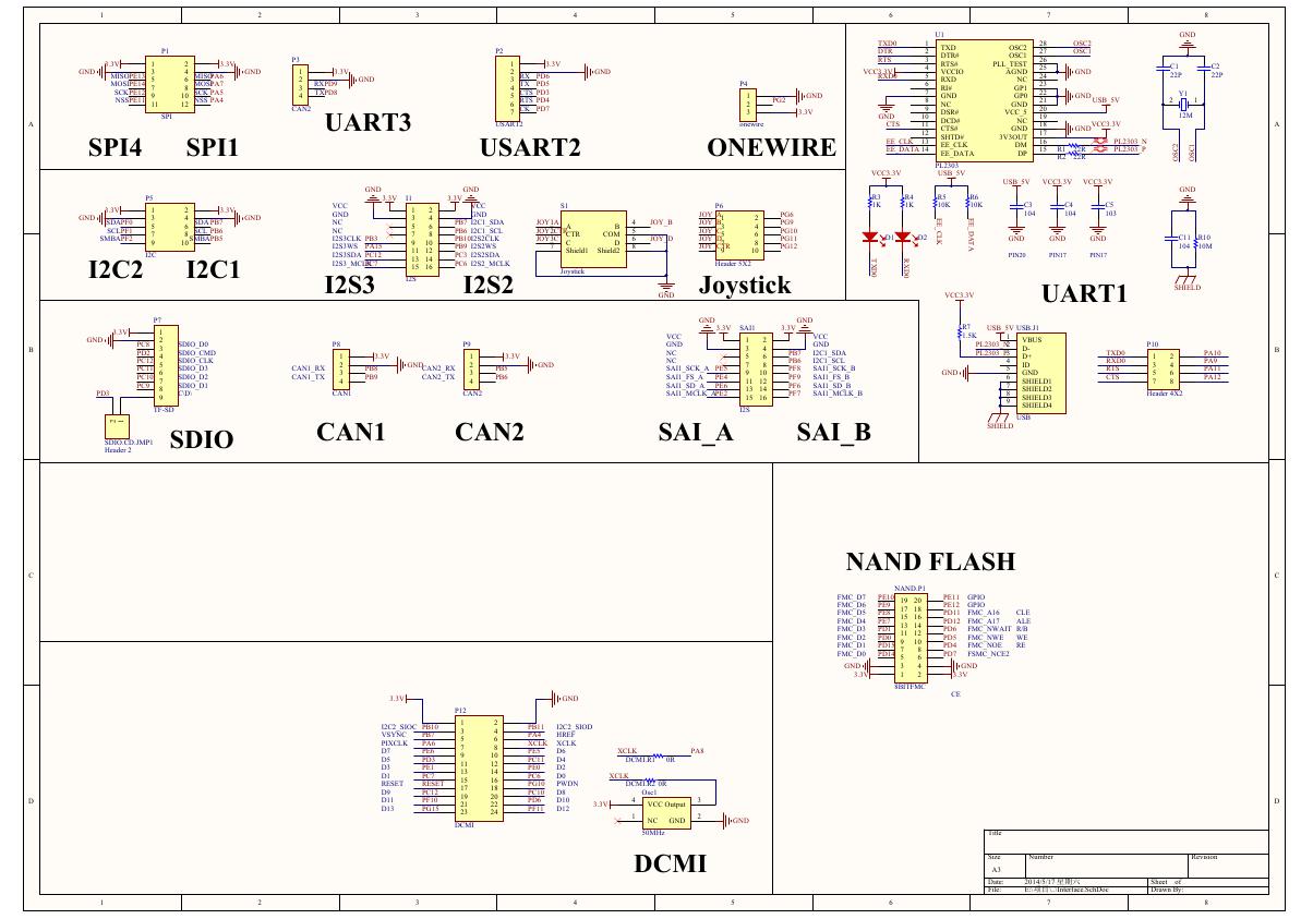 原理图(Open429Z-D-Schematic).pdf
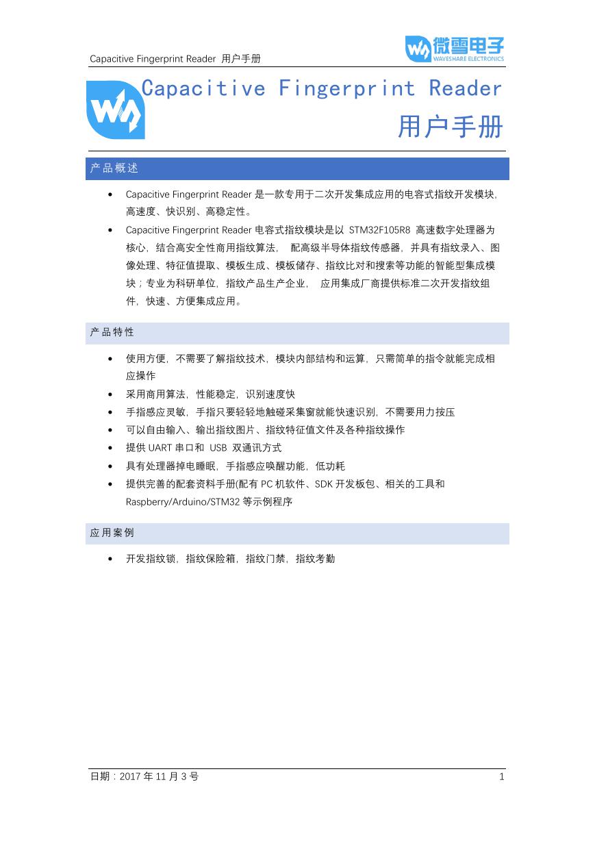 用户手册(Capacitive_Fingerprint_Reader_User_Manual_CN).pdf
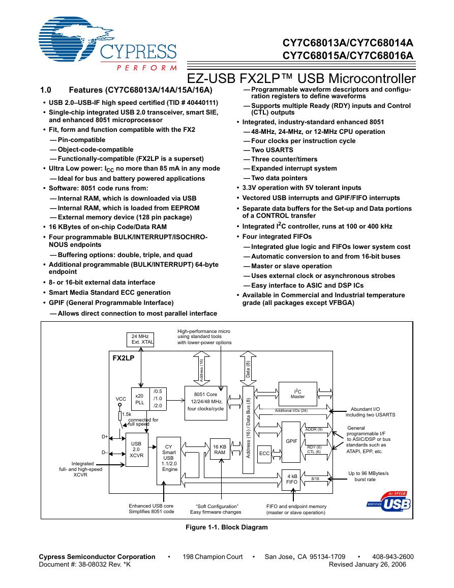 CY7C68013A(英文版)(CY7C68013A).pdf
 TechnicalReference_Dem.pdf