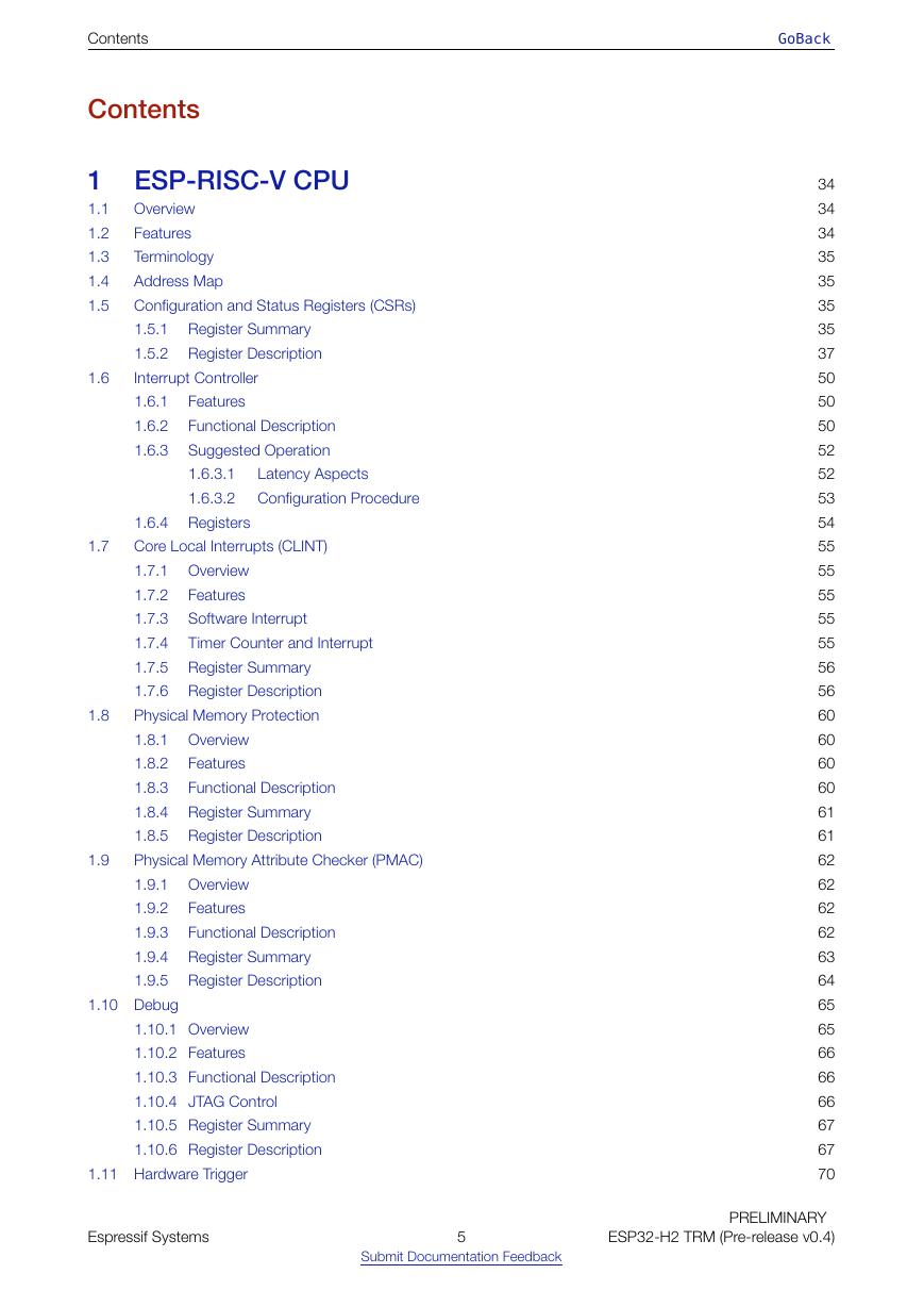
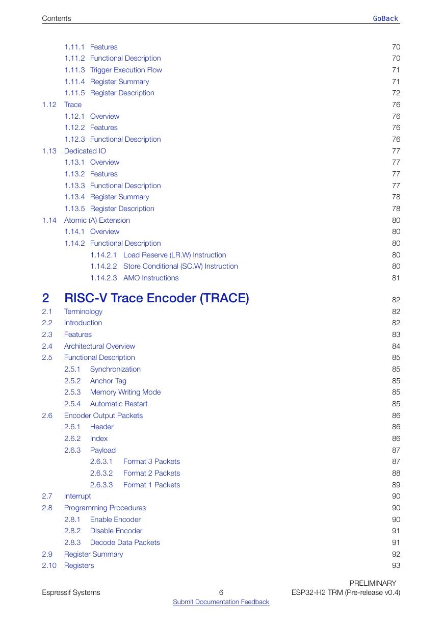
1 ESP-RISC-V CPU
1.1 Overview
1.2 Features
1.3 Terminology
1.4 Address Map
1.5 Configuration and Status Registers (CSRs)
1.5.1 Register Summary
1.5.2 Register Description
1.6 Interrupt Controller
1.6.1 Features
1.6.2 Functional Description
1.6.3 Suggested Operation
1.6.4 Registers
1.7 Core Local Interrupts (CLINT)
1.7.1 Overview
1.7.2 Features
1.7.3 Software Interrupt
1.7.4 Timer Counter and Interrupt
1.7.5 Register Summary
1.7.6 Register Description
1.8 Physical Memory Protection
1.8.1 Overview
1.8.2 Features
1.8.3 Functional Description
1.8.4 Register Summary
1.8.5 Register Description
1.9 Physical Memory Attribute Checker (PMAC)
1.9.1 Overview
1.9.2 Features
1.9.3 Functional Description
1.9.4 Register Summary
1.9.5 Register Description
1.10 Debug
1.10.1 Overview
1.10.2 Features
1.10.3 Functional Description
1.10.4 JTAG Control
1.10.5 Register Summary
1.10.6 Register Description
1.11 Hardware Trigger
1.11.1 Features
1.11.2 Functional Description
1.11.3 Trigger Execution Flow
1.11.4 Register Summary
1.11.5 Register Description
1.12 Trace
1.12.1 Overview
1.12.2 Features
1.12.3 Functional Description
1.13 Dedicated IO
1.13.1 Overview
1.13.2 Features
1.13.3 Functional Description
1.13.4 Register Summary
1.13.5 Register Description
1.14 Atomic (A) Extension
1.14.1 Overview
1.14.2 Functional Description
2 RISC-V Trace Encoder (TRACE)
2.1 Terminology
2.2 Introduction
2.3 Features
2.4 Architectural Overview
2.5 Functional Description
2.5.1 Synchronization
2.5.2 Anchor Tag
2.5.3 Memory Writing Mode
2.5.4 Automatic Restart
2.6 Encoder Output Packets
2.6.1 Header
2.6.2 Index
2.6.3 Payload
2.7 Interrupt
2.8 Programming Procedures
2.8.1 Enable Encoder
2.8.2 Disable Encoder
2.8.3 Decode Data Packets
2.9 Register Summary
2.10 Registers
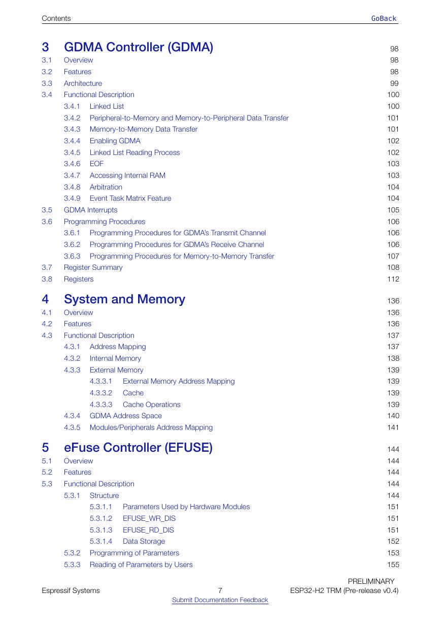
3 GDMA Controller (GDMA)
3.1 Overview
3.2 Features
3.3 Architecture
3.4 Functional Description
3.4.1 Linked List
3.4.2 Peripheral-to-Memory and Memory-to-Peripheral Data Transfer
3.4.3 Memory-to-Memory Data Transfer
3.4.4 Enabling GDMA
3.4.5 Linked List Reading Process
3.4.6 EOF
3.4.7 Accessing Internal RAM
3.4.8 Arbitration
3.4.9 Event Task Matrix Feature
3.5 GDMA Interrupts
3.6 Programming Procedures
3.6.1 Programming Procedures for GDMA's Transmit Channel
3.6.2 Programming Procedures for GDMA's Receive Channel
3.6.3 Programming Procedures for Memory-to-Memory Transfer
3.7 Register Summary
3.8 Registers
4 System and Memory
4.1 Overview
4.2 Features
4.3 Functional Description
4.3.1 Address Mapping
4.3.2 Internal Memory
4.3.3 External Memory
4.3.4 GDMA Address Space
4.3.5 Modules/Peripherals Address Mapping
5 eFuse Controller (EFUSE)
5.1 Overview
5.2 Features
5.3 Functional Description
5.3.1 Structure
5.3.2 Programming of Parameters
5.3.3 Reading of Parameters by Users
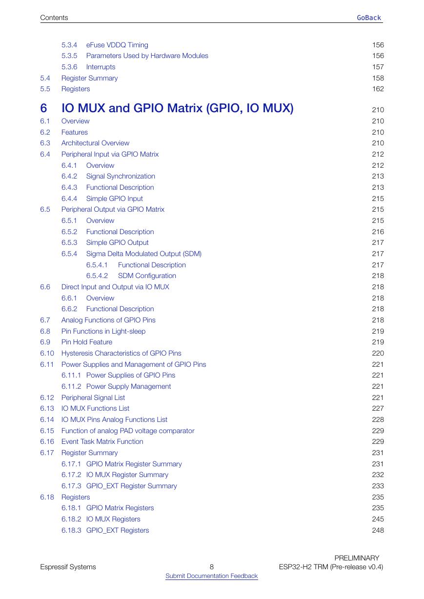
5.3.4 eFuse VDDQ Timing
5.3.5 Parameters Used by Hardware Modules
5.3.6 Interrupts
5.4 Register Summary
5.5 Registers
6 IO MUX and GPIO Matrix (GPIO, IO MUX)
6.1 Overview
6.2 Features
6.3 Architectural Overview
6.4 Peripheral Input via GPIO Matrix
6.4.1 Overview
6.4.2 Signal Synchronization
6.4.3 Functional Description
6.4.4 Simple GPIO Input
6.5 Peripheral Output via GPIO Matrix
6.5.1 Overview
6.5.2 Functional Description
6.5.3 Simple GPIO Output
6.5.4 Sigma Delta Modulated Output (SDM)
6.6 Direct Input and Output via IO MUX
6.6.1 Overview
6.6.2 Functional Description
6.7 Analog Functions of GPIO Pins
6.8 Pin Functions in Light-sleep
6.9 Pin Hold Feature
6.10 Hysteresis Characteristics of GPIO Pins
6.11 Power Supplies and Management of GPIO Pins
6.11.1 Power Supplies of GPIO Pins
6.11.2 Power Supply Management
6.12 Peripheral Signal List
6.13 IO MUX Functions List
6.14 IO MUX Pins Analog Functions List
6.15 Function of analog PAD voltage comparator
6.16 Event Task Matrix Function
6.17 Register Summary
6.17.1 GPIO Matrix Register Summary
6.17.2 IO MUX Register Summary
6.17.3 GPIO_EXT Register Summary
6.18 Registers
6.18.1 GPIO Matrix Registers
6.18.2 IO MUX Registers
6.18.3 GPIO_EXT Registers
7 Reset and Clock
7.1 Reset
7.1.1 Overview
7.1.2 Architectural Overview
7.1.3 Features
7.1.4 Functional Description
7.1.5 Peripheral Reset
7.2 Clock
7.2.1 Overview
7.2.2 Architectural Overview
7.2.3 Features
7.2.4 Functional Description
7.3 Programming Procedures
7.3.1 HP System Clock Configuration
7.3.2 LP System Clock Configuration
7.3.3 Peripheral Clock Reset and Configuration
7.4 Register Summary
7.4.1 PCR Register Summary
7.4.2 LP System Clock Register Summary
7.5 Registers
7.5.1 PCR Registers
7.5.2 LP System Clock Registers
8 Chip Boot Control
8.1 Overview
8.2 Functional Description
8.2.1 Default Configuration
8.2.2 Boot Mode Control
8.2.3 ROM Messages Printing Control
8.2.4 JTAG Signal Source Control
9 Interrupt Matrix (INTMTX)
9.1 Overview
9.2 Interrupt Terminology in ESP32-H2
9.2.1 Interrupt
9.2.2 Interrupt signal/interrupt source
9.2.3 Interrupt Flow in ESP32-H2
9.3 Features
9.4 Architecture
9.5 Functional Description
9.5.1 Peripheral Interrupt Sources
9.5.2 CPU Interrupts
9.5.3 Assign Peripheral Interrupt Source to CPU Interrupt
9.5.4 Query Current Interrupt Status of SOURCE
9.6 Register Summary
9.6.1 Interrupt Matrix Register Summary
9.6.2 Interrupt Priority Register Summary
9.7 Registers
9.7.1 Interrupt Matrix Registers
9.7.2 Interrupt Priority Registers
10 Event Task Matrix (SOC_ETM)
10.1 Overview
10.2 Features
10.3 Functional Description
10.3.1 Architecture
10.3.2 Events
10.3.3 Tasks
10.3.4 Timing Considerations
10.3.5 Channel Control
10.4 Register Summary
10.5 Registers
11 System Timer (SYSTIMER)
11.1 Overview
11.2 Features
11.3 Clock Source Selection
11.4 Functional Description
11.4.1 Counter
11.4.2 Comparator and Alarm
11.4.3 Event Task Matrix
11.4.4 Synchronization Operation
11.4.5 Interrupt
11.5 Programming Procedure
11.5.1 Read Current Count Value
11.5.2 Configure An One-Time Alarm in Target Mode
11.5.3 Configure Periodic Alarms in Period Mode
11.5.4 Update After Deep-sleep and Light-sleep
11.6 Register Summary
11.7 Registers
12 Timer Group (TIMG)
12.1 Overview
12.2 Features
12.3 Functional Description
12.3.1 16-bit Prescaler and Clock Selection
12.3.2 54-bit Time-base Counter
12.3.3 Alarm Generation
12.3.4 Timer Reload
12.3.5 Event Task Matrix Feature
12.3.6 RTC_SLOW_CLK Frequency Calculation
12.3.7 Interrupts
12.4 Configuration and Usage
12.4.1 Timer as a Simple Clock
12.4.2 Timer as One-shot Alarm
12.4.3 Timer as Periodic Alarm by APB
12.4.4 Timer as Periodic Alarm by ETM
12.4.5 RTC_SLOW_CLK Frequency Calculation
12.5 Register Summary
12.6 Registers
13 Watchdog Timers (WDT)
13.1 Overview
13.2 Digital Watchdog Timers
13.2.1 Features
13.2.2 Functional Description
13.3 Super Watchdog
13.3.1 Features
13.3.2 Super Watchdog Controller
13.4 Interrupts
13.5 Register Summary
13.6 Registers
14 Access Permission Management (APM)
14.1 Overview
14.2 Features
14.3 TEE and REE Terminology
14.4 Functional Description
14.4.1 TEE Controller Functional Description
14.4.2 APM Controller Functional Description
14.5 Programming Procedure
14.6 Illegal Access and Interrupts
14.7 Register Summary
14.7.1 APM Registers of HP System (HP_APM_REG)
14.7.2 APM Registers of LP System (LP_APM_REG)
14.7.3 TEE Registers of HP System
14.8 Registers
14.8.1 APM Registers of HP System (HP_APM_REG)
14.8.2 APM Registers of LP System (LP_APM_REG)
14.8.3 TEE Registers of HP System
15 System Registers
15.1 Overview
15.2 Function Description
15.2.1 External Memory Encryption/Decryption Configuration
15.2.2 Anti-DPA Attack Security Control
15.2.3 Software ROM Table Register
15.2.4 Bus Timeout Protection
15.3 Register Summary
15.4 Registers
16 Debug Assistant (ASSIST_DEBUG,MEM_MONITOR)
16.1 Overview
16.2 Features
16.3 Functional Description
16.3.1 Region Read/Write Monitoring
16.3.2 SP Monitoring
16.3.3 PC Logging
16.3.4 CPU/DMA Bus Access Logging
16.4 Recommended Operation
16.4.1 Region Read/Write Monitoring and SP Monitoring Configuration
16.4.2 PC Logging Configuration
16.4.3 CPU/DMA Bus Access Logging Configuration
16.5 Register Summary
16.5.1 Summary of Bus Logging Configuration Registers
16.5.2 Summary of Other Registers
16.6 Registers
16.6.1 Bus Logging Configuration Registers
16.6.2 Other Registers
17 AES Accelerator (AES)
17.1 Introduction
17.2 Features
17.3 Clock and Reset
17.4 AES Working Modes
17.5 Typical AES Working Mode
17.5.1 Key, Plaintext, and Ciphertext
17.5.2 Endianness
17.5.3 Operation Process
17.6 DMA-AES Working Mode
17.6.1 Key, Plaintext, and Ciphertext
17.6.2 Endianness
17.6.3 Standard Incrementing Function
17.6.4 Block Number
17.6.5 Initialization Vector
17.6.6 Block Operation Process
17.7 Memory Summary
17.8 Register Summary
17.9 Registers
18 ECC Accelerator (ECC)
18.1 Introduction
18.2 Features
18.3 ECC Basics
18.3.1 Elliptic Curve and Points on the Curves
18.3.2 Affine Coordinates and Jacobian Coordinates
18.3.3 Memory Blocks
18.3.4 Data and Data Block
18.3.5 Writing Data
18.3.6 Reading Data
18.3.7 Standard Calculation and Jacobian Calculation
18.4 Function Description
18.4.1 Key Size
18.4.2 Working Modes
18.5 Clock and Reset
18.6 Interrupts
18.7 Programming Procedures
18.8 Register Summary
18.9 Registers
19 HMAC Accelerator (HMAC)
19.1 Main Features
19.2 Functional Description
19.2.1 Upstream Mode
19.2.2 Downstream JTAG Enable Mode
19.2.3 Downstream Digital Signature Algorithm Mode
19.2.4 HMAC eFuse Configuration
19.2.5 HMAC Process (Detailed)
19.3 HMAC Algorithm Details
19.3.1 Padding Bits
19.3.2 HMAC Algorithm Structure
19.4 Register Summary
19.5 Registers
20 RSA Accelerator (RSA)
20.1 Introduction
20.2 Features
20.3 Functional Description
20.3.1 Large-Number Modular Exponentiation
20.3.2 Large-Number Modular Multiplication
20.3.3 Large-Number Multiplication
20.3.4 Options for Additional Acceleration
20.4 Memory Summary
20.5 Register Summary
20.6 Registers
21 SHA Accelerator (SHA)
21.1 Introduction
21.2 Features
21.3 Working Modes
21.4 Function Description
21.4.1 Preprocessing
21.4.2 Hash Operation
21.4.3 Message Digest
21.4.4 Interrupt
21.5 Register Summary
21.6 Registers
22 Digital Signature Algorithm (DSA)
22.1 Overview
22.2 Features
22.3 Functional Description
22.3.1 Overview
22.3.2 Private Key Operands
22.3.3 Software Prerequisites
22.3.4 DSA Operation at the Hardware Level
22.3.5 DSA Operation at the Software Level
22.4 Memory Summary
22.5 Register Summary
22.6 Registers
23 Elliptic Curve Digital Signature Algorithm (ECDSA)
23.1 Introduction
23.2 Features
23.3 ECDSA Basics
23.3.1 Domain Parameters
23.3.2 Key Generation
23.3.3 Signature Generation
23.3.4 Signature Verification
23.4 Functional Description
23.4.1 ECDSA Working Modes
23.4.2 Data and Data Block
23.4.3 Security Features
23.5 Programming Procedures
23.5.1 ECDSA Process
23.5.2 Clocks and Resets
23.5.3 Interrupts
23.6 Memory Blocks
23.7 Register Summary
23.8 Registers
24 External Memory Encryption and Decryption (XTS_AES)
24.1 Overview
24.2 Features
24.3 Module Structure
24.4 Functional Description
24.4.1 XTS Algorithm
24.4.2 Key
24.4.3 Target Memory Space
24.4.4 Data Writing
24.4.5 Manual Encryption Block
24.4.6 Auto Decryption Block
24.5 Software Process
24.6 Anti-DPA
24.7 Register Summary
24.8 Registers
25 UART Controller (UART)
25.1 Overview
25.2 Features
25.3 UART Structure
25.4 Functional Description
25.4.1 Clock and Reset
25.4.2 UART FIFO
25.4.3 Baud Rate Generation and Detection
25.4.4 UART Data Frame
25.4.5 AT_CMD Character Stucture
25.4.6 RS485
25.4.7 IrDA
25.4.8 Wake-up
25.4.9 Flow Control
25.4.10 GDMA Mode
25.4.11 UART Interrupts
25.4.12 UHCI Interrupts
25.5 Programming Procedures
25.5.1 Register Type
25.5.2 Detailed Steps
25.6 Register Summary
25.6.1 UART Register Summary
25.6.2 UHCI Register Summary
25.7 Registers
25.7.1 UART Registers
25.7.2 UHCI Registers
26 SPI Controller (SPI)
26.1 Overview
26.2 Glossary
26.3 Features
26.4 Architectural Overview
26.5 Functional Description
26.5.1 Data Modes
26.5.2 Introduction to FSPI Bus Signals
26.5.3 Bit Read/Write Order Control
26.5.4 Transfer Types
26.5.5 CPU-Controlled Data Transfer
26.5.6 DMA-Controlled Data Transfer
26.5.7 Data Flow Control
26.5.8 GP-SPI2 as a Master
26.5.9 GP-SPI2 Works as a Slave
26.6 CS Setup Time and Hold Time Control
26.7 GP-SPI2 Clock Control
26.7.1 Clock Phase and Polarity
26.7.2 Clock Control as Master
26.7.3 Clock Control as Slave
26.8 Interrupts
26.9 Register Summary
26.10 Registers
27 I2C Controller (I2C)
27.1 Overview
27.2 Features
27.3 I2C Architecture
27.4 Functional Description
27.4.1 Clock Configuration
27.4.2 SCL and SDA Noise Filtering
27.4.3 SCL Clock Stretching
27.4.4 Generating SCL Pulses in Idle State
27.4.5 Synchronization
27.4.6 Open-Drain Output
27.4.7 Timing Parameter Configuration
27.4.8 Timeout Control
27.4.9 Command Configuration
27.4.10 TX/RX RAM Data Storage
27.4.11 Data Conversion
27.4.12 Addressing Mode
27.4.13 R/W Bit Check in 10-bit Addressing Mode
27.4.14 To Start the I2C Controller
27.5 Programming Example
27.5.1 I2C master Writes to I2C slave with a 7-bit Address in One Command Sequence
27.5.2 I2C master Writes to I2C slave with a 10-bit Address in One Command Sequence
27.5.3 I2C master Writes to I2C slave with Two 7-bit Addresses in One Command Sequence
27.5.4 I2C master Writes to I2C slave with a 7-bit Address in Multiple Command Sequences
27.5.5 I2C master Reads I2C slave with a 7-bit Address in One Command Sequence
27.5.6 I2C master Reads I2C slave with a 10-bit Address in One Command Sequence
27.5.7 I2C master Reads I2C slave with Two 7-bit Addresses in One Command Sequence
27.5.8 I2C master Reads I2C slave with a 7-bit Address in Multiple Command Sequences
27.6 Interrupts
27.7 Register Summary
27.8 Registers
28 I2S Controller (I2S)
28.1 Overview
28.2 Terminology
28.3 Features
28.4 System Architecture
28.5 Supported Audio Standards
28.5.1 TDM Philips Standard
28.5.2 TDM MSB Alignment Standard
28.5.3 TDM PCM Standard
28.5.4 PDM Standard
28.6 I2S TX/RX Clock
28.7 I2S Reset
28.8 I2S Master/Slave Mode
28.8.1 Master/Slave TX Mode
28.8.2 Master/Slave RX Mode
28.9 Transmitting Data
28.9.1 Data Format Control
28.9.2 Channel Mode Control
28.10 Receiving Data
28.10.1 Channel Mode Control
28.10.2 Data Format Control
28.11 Software Configuration Process
28.11.1 Configure I2S as TX Mode
28.11.2 Configure I2S as RX Mode
28.12 I2S Interrupts
28.12.1 Event Task Matrix Feature
28.13 Register Summary
28.14 Registers
29 Pulse Count Controller (PCNT)
29.1 Features
29.2 Functional Description
29.3 Applications
29.3.1 Channel 0 Incrementing Independently
29.3.2 Channel 0 Decrementing Independently
29.3.3 Channel 0 and Channel 1 Incrementing Together
29.4 Register Summary
29.5 Registers
30 USB Serial/JTAG Controller (USB_SERIAL_JTAG)
30.1 Overview
30.2 Features
30.3 Functional Description
30.3.1 CDC-ACM USB Interface Functional Description
30.3.2 CDC-ACM Firmware Interface Functional Description
30.3.3 USB-to-JTAG Interface: JTAG Command Processor
30.3.4 USB-to-JTAG Interface: CMD_REP Usage Example
30.3.5 USB-to-JTAG Interface: Response Capture Unit
30.3.6 USB-to-JTAG Interface: Control Transfer Requests
30.4 Recommended Operation
30.5 Interrupts
30.6 Register Summary
30.7 Registers
31 Two-wire Automotive Interface (TWAI)
31.1 Features
31.2 Protocol Overview
31.2.1 TWAI Properties
31.2.2 TWAI Messages
31.2.3 TWAI Errors
31.2.4 TWAI Bit Timing
31.3 Architectural Overview
31.3.1 Registers Block
31.3.2 Bit Stream Processor
31.3.3 Error Management Logic
31.3.4 Bit Timing Logic
31.3.5 Acceptance Filter
31.3.6 Receive FIFO
31.4 Functional Description
31.4.1 Modes
31.4.2 Bit Timing
31.4.3 Interrupt Management
31.4.4 Transmit and Receive Buffers
31.4.5 Receive FIFO and Data Overruns
31.4.6 Acceptance Filter
31.4.7 Error Management
31.4.8 Error Code Capture
31.4.9 Arbitration Lost Capture
31.4.10 Transceiver Auto-Standby
31.5 Register Summary
31.6 Registers
32 LED PWM Controller (LEDC)
32.1 Overview
32.2 Features
32.3 Functional Description
32.3.1 Architecture
32.3.2 Timers
32.3.3 PWM Generators
32.3.4 Duty Cycle Fading
32.3.5 Event Task Matrix Feature
32.3.6 Interrupts
32.4 Register Summary
32.5 Registers
33 Motor Control PWM (MCPWM)
33.1 Overview
33.2 Features
33.3 Modules
33.3.1 Overview
33.3.2 PWM Timer Module
33.3.3 PWM Operator Module
33.3.4 Capture Module
33.3.5 ETM Module
33.3.6 Interrupts
33.4 Register Summary
33.5 Registers
34 Remote Control Peripheral (RMT)
34.1 Overview
34.2 Features
34.3 Functional Description
34.3.1 RMT Architecture
34.3.2 RMT RAM
34.3.3 Clock
34.3.4 Transmitter
34.3.5 Receiver
34.3.6 Configuration Update
34.3.7 Interrupts
34.4 Register Summary
34.5 Registers
35 Parallel IO Controller (PARL_IO)
35.1 Introduction
35.2 Glossary
35.3 Features
35.4 Architectural Overview
35.5 Functional Description
35.5.1 Clock Generator
35.5.2 Clock & Reset Restriction
35.5.3 Master-Slave Mode
35.5.4 Receive Modes of the RX Unit
35.5.5 RX Unit GDMA SUC EOF Generation
35.5.6 RX Unit Timeout
35.5.7 Output Clock Gating of TX Unit
35.5.8 Valid Signal Output of TX Unit
35.5.9 Bus Idle Value of TX Unit
35.5.10 Data Transfer in a Single Frame
35.5.11 Bit Reversal in One Byte
35.6 Programming Procedures
35.6.1 Data Receiving Operation Process
35.6.2 Data Transmitting Operation Process
35.7 Application Examples
35.7.1 Co-working with SPI
35.7.2 Co-working with I2S
35.8 Interrupts
35.9 Register Summary
35.10 Registers
36 SAR ADC and Temperature Sensor
36.1 Overview
36.2 SAR ADC
36.2.1 Introduction
36.2.2 Features
36.2.3 Architecture
36.2.4 Functional Description
36.2.5 Programming Procedure
36.2.6 Interrupts
36.3 Temperature Sensor
36.3.1 Overview
36.3.2 Features
36.3.3 Architecture
36.3.4 Functional Description
36.3.5 Programming Procedure
36.3.6 Interrupts
36.4 Event Task Matrix Feature
36.4.1 SAR ADC's ETM Feature
36.4.2 Temperature Sensor's ETM Feature
36.5 Register Summary
36.6 Registers
37 Related Documentation and Resources
Glossary
Abbreviations for Peripherals
Abbreviations Related to Registers
Access Types for Registers
Programming Reserved Register Field
Introduction
Programming Reserved Register Field
Interrupt Configuration Registers
Revision History



 V2版本原理图(Capacitive-Fingerprint-Reader-Schematic_V2).pdf
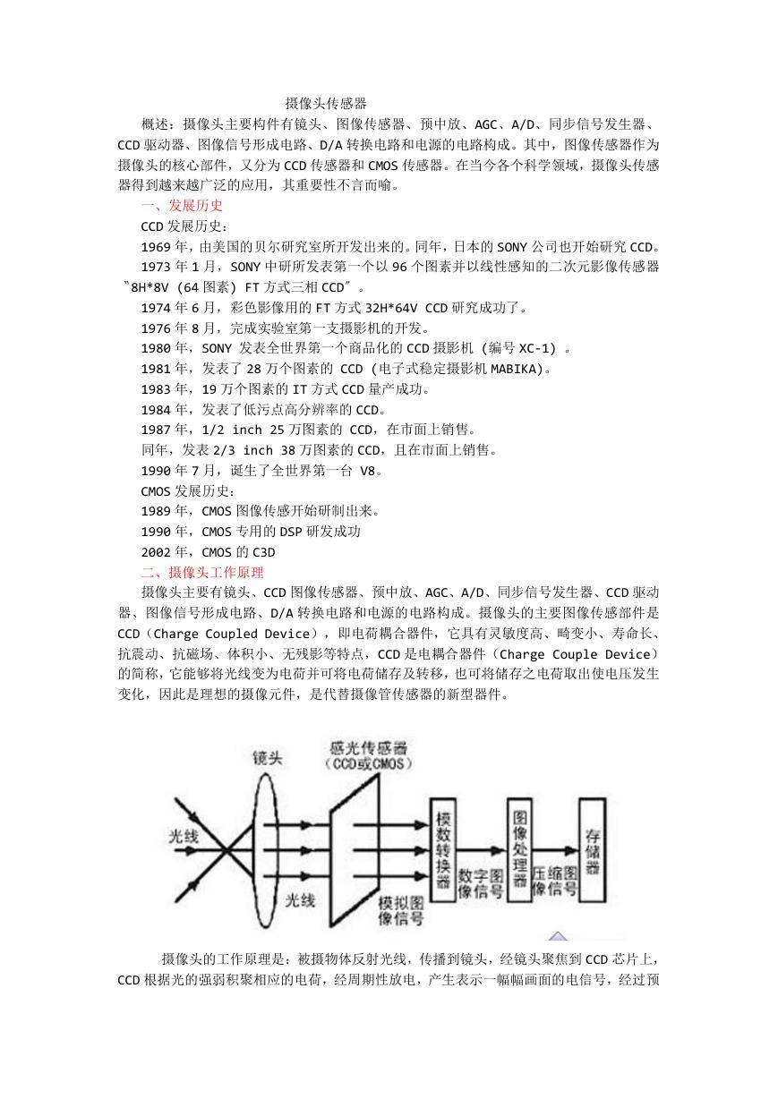 摄像头工作原理.doc
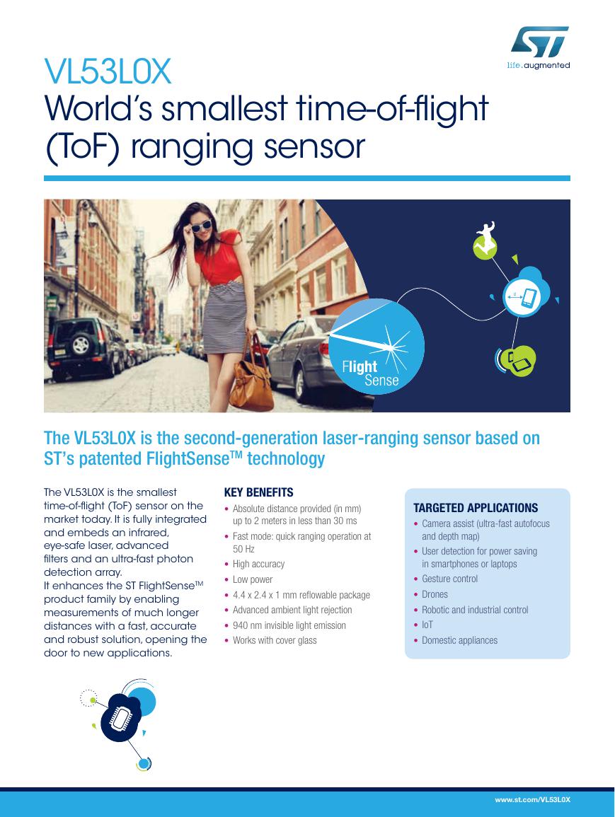 VL53L0X简要说明(En.FLVL53L00216).pdf
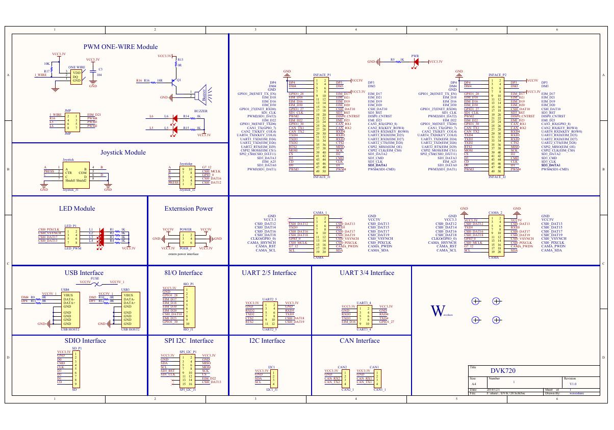 原理图(DVK720-Schematic).pdf
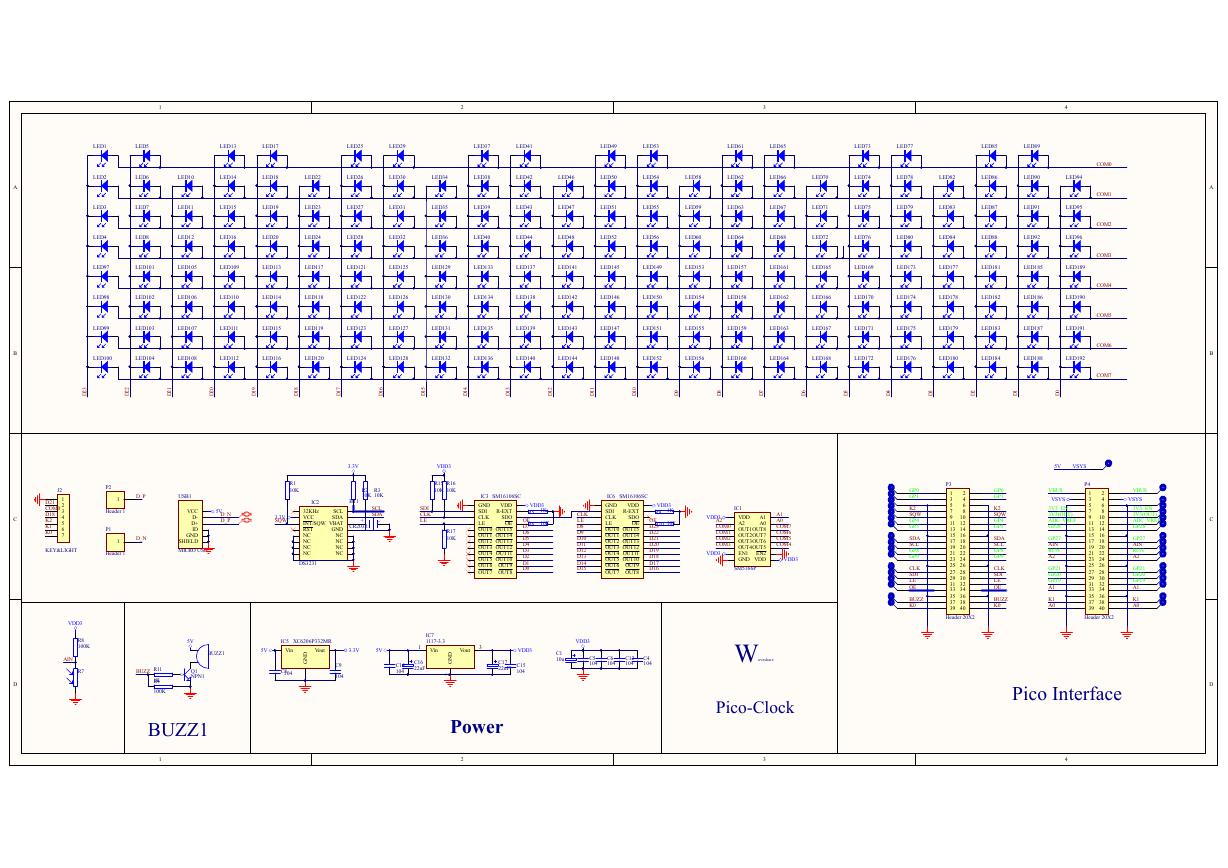 原理图(Pico-Clock-Green-Schdoc).pdf
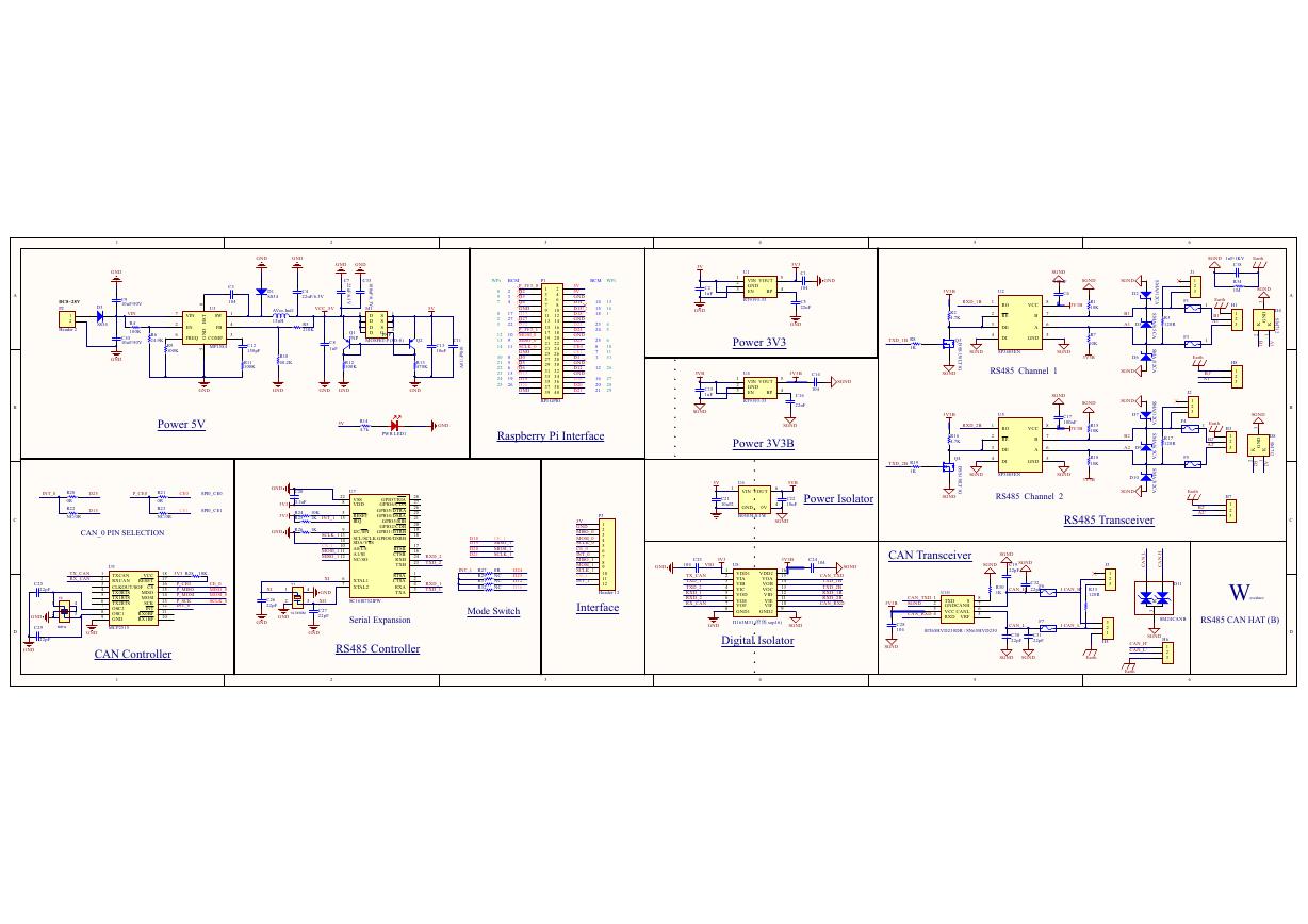 原理图(RS485-CAN-HAT-B-schematic).pdf
 File:SIM7500_SIM7600_SIM7800 Series_SSL_Application Note_V2.00.pdf
 ADS1263(Ads1262).pdf
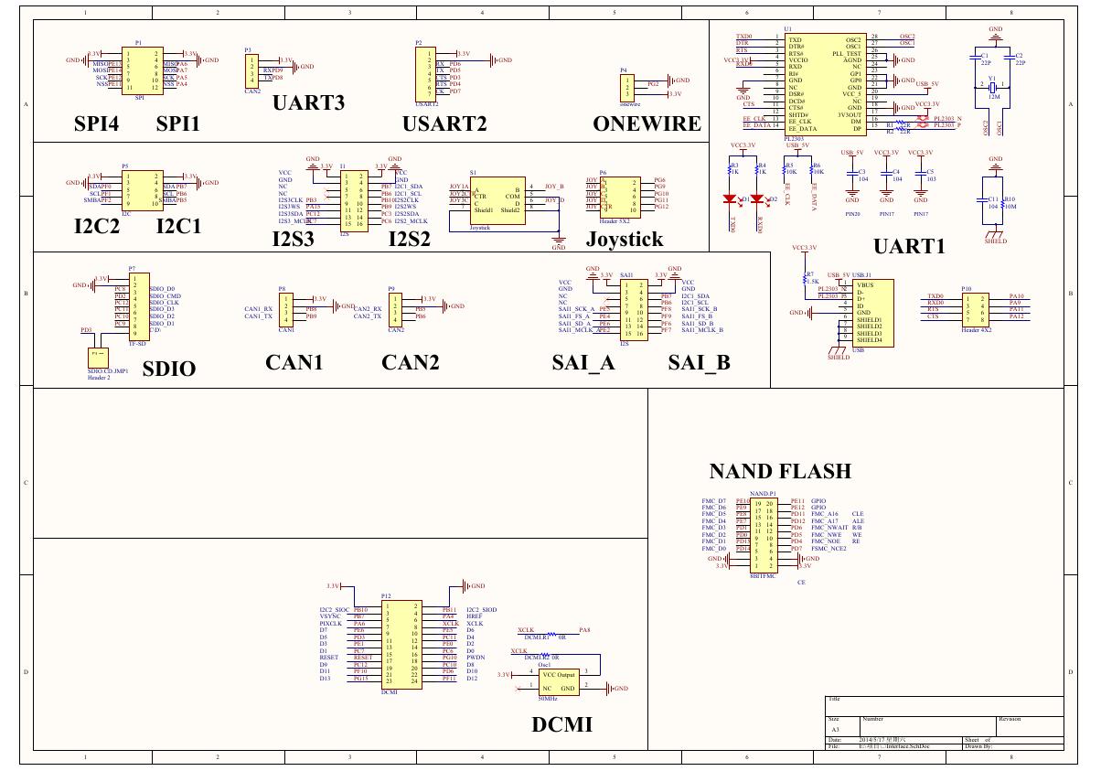 原理图(Open429Z-D-Schematic).pdf
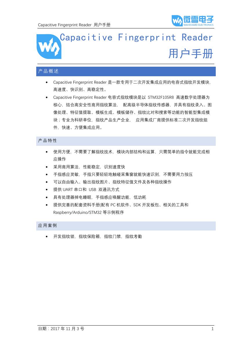 用户手册(Capacitive_Fingerprint_Reader_User_Manual_CN).pdf
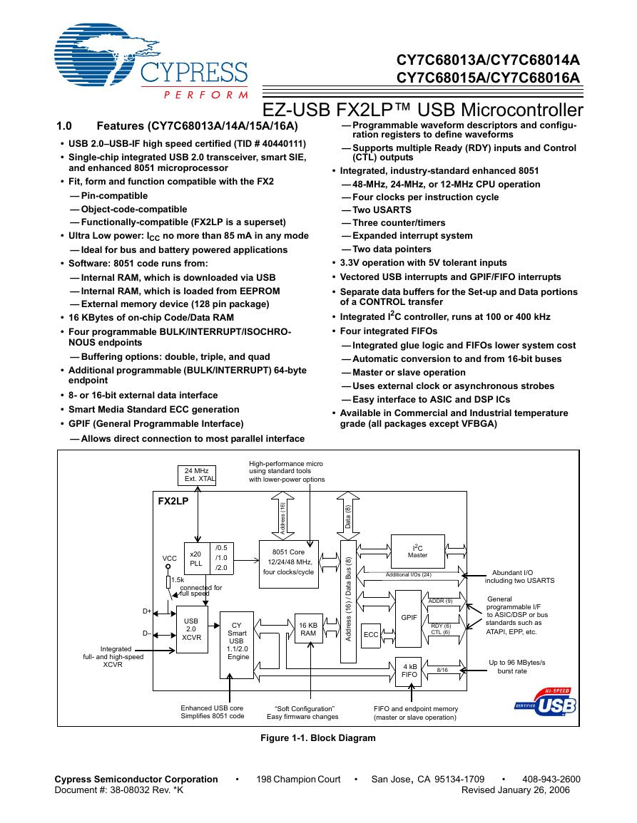 CY7C68013A(英文版)(CY7C68013A).pdf
 TechnicalReference_Dem.pdf