S-8261 Series
BATTERY PROTECTION IC FOR 1-CELL PACK
Rev.5.3_00
www.sii-ic.com
© Seiko Instruments Inc., 2001-2012
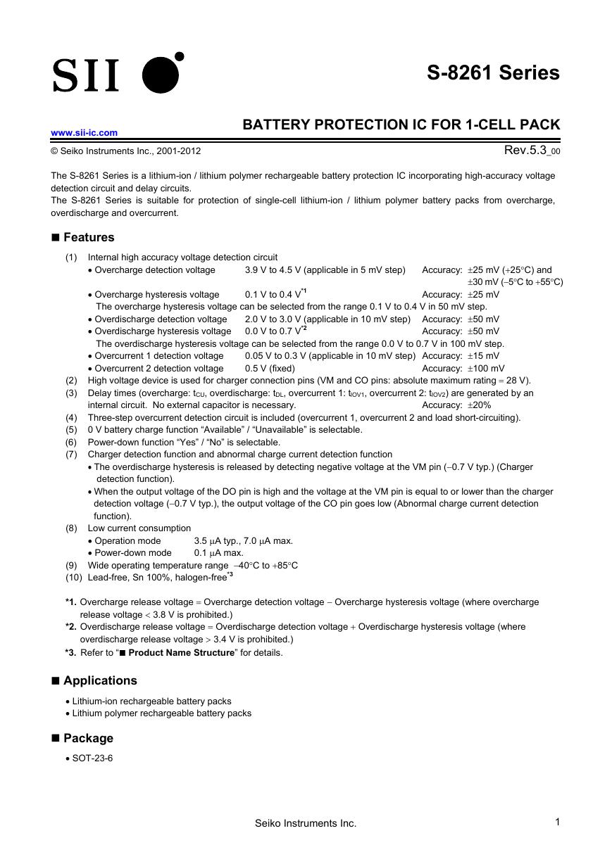
The S-8261 Series is a lithium-ion / lithium polymer rechargeable battery protection IC incorporating high-accuracy voltage
detection circuit and delay circuits.
The S-8261 Series is suitable for protection of single-cell lithium-ion / lithium polymer battery packs from overcharge,
overdischarge and overcurrent.
Features
(1)
Internal high accuracy voltage detection circuit
• Overcharge detection voltage
• Overcharge hysteresis voltage
3.9 V to 4.5 V (applicable in 5 mV step)
0.1 V to 0.4 V*1
Accuracy: ±25 mV (+25°C) and
Accuracy: ±25 mV
±30 mV (−5°C to +55°C)
The overcharge hysteresis voltage can be selected from the range 0.1 V to 0.4 V in 50 mV step.
• Overdischarge detection voltage 2.0 V to 3.0 V (applicable in 10 mV step) Accuracy: ±50 mV
• Overdischarge hysteresis voltage 0.0 V to 0.7 V*2
Accuracy: ±50 mV
The overdischarge hysteresis voltage can be selected from the range 0.0 V to 0.7 V in 100 mV step.
0.05 V to 0.3 V (applicable in 10 mV step) Accuracy: ±15 mV
0.5 V (fixed)
Accuracy: ±100 mV
• Overcurrent 1 detection voltage
• Overcurrent 2 detection voltage
(2) High voltage device is used for charger connection pins (VM and CO pins: absolute maximum rating = 28 V).
(3) Delay times (overcharge: tCU, overdischarge: tDL, overcurrent 1: tlOV1, overcurrent 2: tlOV2) are generated by an
internal circuit. No external capacitor is necessary.
Accuracy: ±20%
(4) Three-step overcurrent detection circuit is included (overcurrent 1, overcurrent 2 and load short-circuiting).
(5) 0 V battery charge function “Available” / “Unavailable” is selectable.
(6) Power-down function “Yes” / “No” is selectable.
(7) Charger detection function and abnormal charge current detection function
• The overdischarge hysteresis is released by detecting negative voltage at the VM pin (−0.7 V typ.) (Charger
detection function).
• When the output voltage of the DO pin is high and the voltage at the VM pin is equal to or lower than the charger
detection voltage (−0.7 V typ.), the output voltage of the CO pin goes low (Abnormal charge current detection
function).
(8) Low current consumption
• Operation mode
• Power-down mode
3.5 μA typ., 7.0 μA max.
0.1 μA max.
(9) Wide operating temperature range −40°C to +85°C
(10) Lead-free, Sn 100%, halogen-free*3
*1. Overcharge release voltage = Overcharge detection voltage − Overcharge hysteresis voltage (where overcharge
release voltage < 3.8 V is prohibited.)
*2. Overdischarge release voltage = Overdischarge detection voltage + Overdischarge hysteresis voltage (where
overdischarge release voltage > 3.4 V is prohibited.)
*3. Refer to “ Product Name Structure” for details.
Applications
• Lithium-ion rechargeable battery packs
• Lithium polymer rechargeable battery packs
Package
• SOT-23-6
Seiko Instruments Inc.
1
�
BATTERY PROTECTION IC FOR 1-CELL PACK
S-8261 Series
Rev.5.3_00
Block Diagram
DO
CO
VM
RVMD
RVMS
DP
Output control circuit
0 V battery charge circuit
or 0 V battery charge
inhibition circuit
Divider control
circuit
Oscillator control
circuit
Charger detection circuit
+
-
Overcurrent 1
detection comparator
+
-
Overcurrent 2
detection comparator
+
-
Load short-circuiting detection comparator
+
-
Overcharge
detection
comparator
+
-
Overdischarge
detection
comparator
Remark All the diodes shown in the figure are parasitic diodes.
Figure 1
VDD
VSS
2
Seiko Instruments Inc.
�
BATTERY PROTECTION IC FOR 1-CELL PACK
S-8261 Series
Rev.5.3_00
Product Name Structure
1. Product Name
S-8261A xx MD - xxx T2 x
U: Lead-free (Sn 100%), halogen-free
S: Lead-free, halogen-free
G: Lead-free (for details, please contact our sales office)
Environmental code
IC direction in tape specifications*1
Product name (abbreviation)*2
Package name (abbreviation)
Serial code
MD: SOT-23-6
Assigned from AA to ZZ in alphabetical order
*1. Refer to the tape drawing.
*2. Refer to the “3. Product Name List”.
2. Package
Package name
SOT-23-6
Package
MP006-A-P-SD
Drawing code
Tape
MP006-A-C-SD
Reel
MP006-A-R-SD
Seiko Instruments Inc.
3
�
BATTERY PROTECTION IC FOR 1-CELL PACK
S-8261 Series
Rev.5.3_00
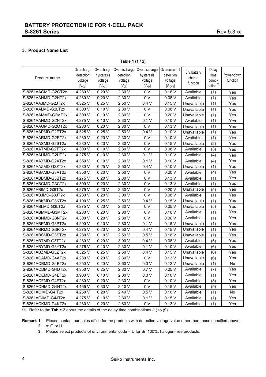
3. Product Name List
Product name
Overcharge
detection
voltage
[VCU]
Table 1 (1 / 2)
Overdischarge
Overdischarge
Overcurrent 1
0 V battery
charge
function
Delay
time
combi-
nation *1
Power-down
function
Overcharge
hysteresis
voltage
[VHC]
0.20 V
0.20 V
0.25 V
0.10 V
0.10 V
0.10 V
0.20 V
0.25 V
0.20 V
0.20 V
0.10 V
0.10 V
0.10 V
0.25 V
0.20 V
0.20 V
0.20 V
0.20 V
0.20 V
0.25 V
0.20 V
0.20 V
0.20 V
0.10 V
0.20 V
0.10 V
0.20 V
0.10 V
0.25 V
0.20 V
0.20 V
0.25 V
0.10 V
0.20 V
0.30 V
0.20 V
0.10 V
0.20 V
4.280 V
4.280 V
4.325 V
4.300 V
4.300 V
4.275 V
4.280 V
4.325 V
4.280 V
4.280 V
4.300 V
4.275 V
4.350 V
4.280 V
4.350 V
4.275 V
4.300 V
4.275 V
4.280 V
4.100 V
4.275 V
4.280 V
4.300 V
4.200 V
4.275 V
4.280 V
4.280 V
4.275 V
4.325 V
4.280 V
4.250 V
4.350 V
3.900 V
4.280 V
4.465 V
4.250 V
4.275 V
4.280 V
detection
voltage
[VDL]
2.30 V
2.30 V
2.50 V
2.30 V
2.30 V
2.30 V
2.30 V
2.50 V
2.30 V
2.30 V
2.30 V
2.30 V
2.30 V
2.50 V
2.50 V
2.30 V
2.30 V
2.30 V
3.00 V
2.50 V
2.30 V
2.80 V
2.30 V
2.80 V
2.50 V
2.50 V
3.00 V
2.30 V
2.50 V
2.30 V
2.60 V
2.30 V
2.00 V
2.30 V
2.10 V
2.40 V
2.30 V
2.80 V
detection
voltage
[VIOV1]
Available
0.16 V
0.08 V
Available
0.15 V Unavailable
0.08 V Unavailable
0.20 V Unavailable
0.10 V
Available
0.13 V Unavailable
0.10 V Unavailable
0.10 V
Available
0.15 V Unavailable
0.08 V
Available
Available
0.10 V
0.10 V
Available
0.10 V Unavailable
0.20 V
Available
Available
0.13 V
0.13 V
Available
0.20 V Unavailable
0.08 V
Available
0.15 V Unavailable
0.05 V Unavailable
Available
0.10 V
Available
0.06 V
0.15 V Unavailable
0.15 V Unavailable
0.18 V Unavailable
Available
0.08 V
Available
0.10 V
0.15 V Unavailable
0.13 V Unavailable
0.12 V Unavailable
Available
0.25 V
Available
0.10 V
Available
0.10 V
Available
0.15 V
Available
0.10 V
Available
0.15 V
0.13 V
Available
S-8261AAGMD-G2GT2x
S-8261AAHMD-G2HT2x
S-8261AAJMD-G2JT2x
S-8261AALMD-G2LT2x
S-8261AAMMD-G2MT2x
S-8261AANMD-G2NT2x
S-8261AAOMD-G2OT2x
S-8261AAPMD-G2PT2x
S-8261AARMD-G2RT2x
S-8261AASMD-G2ST2x
S-8261AATMD-G2TT2x
S-8261AAUMD-G2UT2x
S-8261AAXMD-G2XT2x
S-8261AAZMD-G2ZT2x
S-8261ABAMD-G3AT2x
S-8261ABBMD-G3BT2x
S-8261ABCMD-G3CT2x
S-8261ABIMD-G3IT2x
S-8261ABJMD-G3JT2x
S-8261ABKMD-G3KT2x
S-8261ABLMD-G3LT2x
S-8261ABMMD-G3MT2x
S-8261ABNMD-G3NT2x
S-8261ABPMD-G3PT2x
S-8261ABRMD-G3RT2x
S-8261ABSMD-G3ST2x
S-8261ABTMD-G3TT2x
S-8261ABYMD-G3YT2x
S-8261ABZMD-G3ZT2x
S-8261ACAMD-G4AT2x
S-8261ACBMD-G4BT2x
S-8261ACDMD-G4DT2x
S-8261ACEMD-G4ET2x
S-8261ACFMD-G4FT2x
S-8261ACHMD-G4HT2x
S-8261ACIMD-G4IT2x
S-8261ACJMD-G4JT2x
S-8261ACKMD-G4KT2x
*1. Refer to the Table 2 about the details of the delay time combinations (1) to (9).
Remark 1. Please contact our sales office for the products with detection voltage value other than those specified above.
hysteresis
voltage
[VHD]
0 V
0 V
0.4 V
0 V
0 V
0.1 V
0 V
0.4 V
0 V
0 V
0 V
0.1 V
0.1 V
0.4 V
0 V
0 V
0 V
0 V
0 V
0.4 V
0 V
0 V
0 V
0.1 V
0.4 V
0.5 V
0.4 V
0.1 V
0.4 V
0 V
0.3 V
0.7 V
0.3 V
0 V
0 V
0.5 V
0.1 V
0 V
2. x: G or U
3. Please select products of environmental code = U for Sn 100%, halogen-free products.
(1)
(1)
(1)
(1)
(1)
(1)
(1)
(1)
(1)
(2)
(3)
(4)
(4)
(1)
(4)
(1)
(1)
(5)
(1)
(1)
(5)
(1)
(1)
(1)
(1)
(1)
(5)
(6)
(6)
(6)
(1)
(7)
(1)
(8)
(9)
(1)
(1)
(1)
Yes
Yes
Yes
Yes
Yes
Yes
Yes
Yes
Yes
Yes
Yes
Yes
Yes
Yes
Yes
Yes
Yes
Yes
Yes
Yes
Yes
Yes
Yes
Yes
Yes
Yes
Yes
Yes
Yes
Yes
No
Yes
Yes
Yes
Yes
No
Yes
Yes
4
Seiko Instruments Inc.
�
BATTERY PROTECTION IC FOR 1-CELL PACK
S-8261 Series
Rev.5.3_00
Product name
Overcharge
detection
voltage
[VCU]
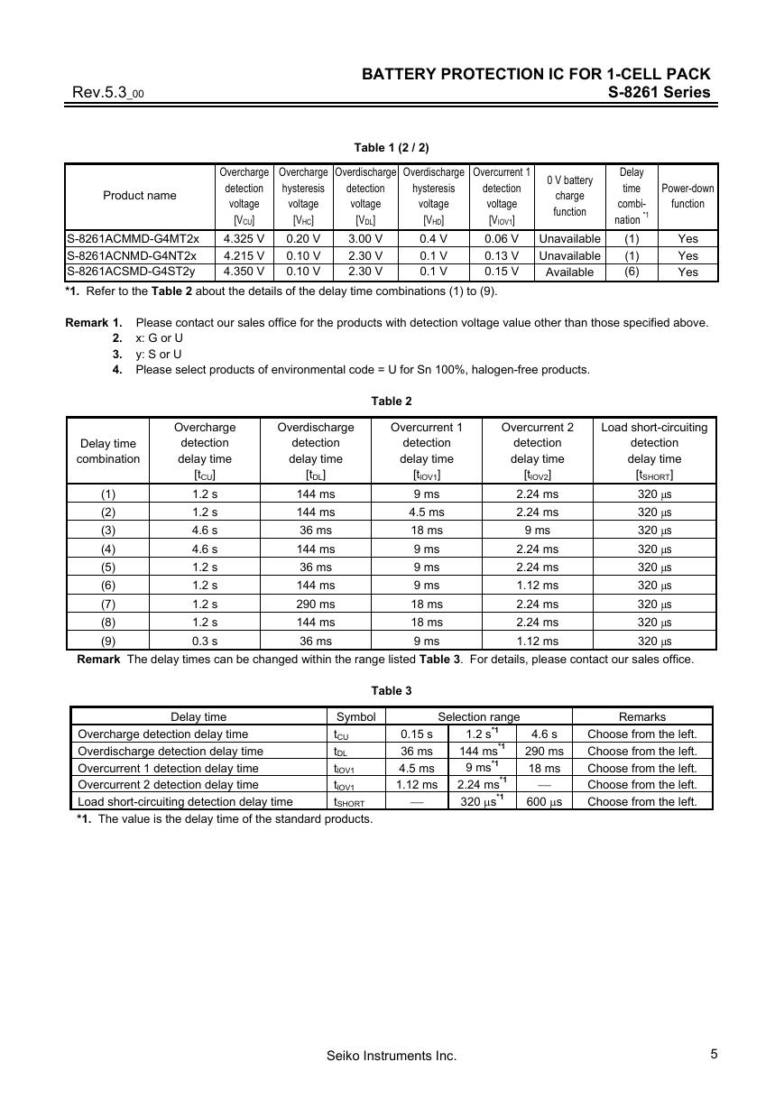
Table 1 (2 / 2)
Overdischarge
Overdischarge
Overcurrent 1
Overcharge
hysteresis
voltage
[VHC]
0.20 V
0.10 V
0.10 V
detection
voltage
[VDL]
3.00 V
2.30 V
2.30 V
hysteresis
voltage
[VHD]
0.4 V
0.1 V
0.1 V
0 V battery
charge
function
detection
voltage
[VIOV1]
0.06 V Unavailable
0.13 V Unavailable
0.15 V
Available
Delay
time
combi-
nation *1
Power-down
function
4.325 V
4.215 V
4.350 V
S-8261ACMMD-G4MT2x
S-8261ACNMD-G4NT2x
S-8261ACSMD-G4ST2y
*1. Refer to the Table 2 about the details of the delay time combinations (1) to (9).
Remark 1. Please contact our sales office for the products with detection voltage value other than those specified above.
2. x: G or U
3. y: S or U
4. Please select products of environmental code = U for Sn 100%, halogen-free products.
(1)
(1)
(6)
Yes
Yes
Yes
Delay time
combination
(1)
(2)
(3)
(4)
(5)
(6)
(7)
(8)
(9)
Overcharge
detection
delay time
[tCU]
1.2 s
1.2 s
4.6 s
4.6 s
1.2 s
1.2 s
1.2 s
1.2 s
0.3 s
Table 2
Overdischarge
Overcurrent 1
detection
delay time
detection
delay time
[tDL]
144 ms
144 ms
36 ms
144 ms
36 ms
144 ms
290 ms
144 ms
36 ms
[tlOV1]
9 ms
4.5 ms
18 ms
9 ms
9 ms
9 ms
18 ms
18 ms
9 ms
Overcurrent 2
detection
delay time
[tlOV2]
2.24 ms
2.24 ms
9 ms
2.24 ms
2.24 ms
1.12 ms
2.24 ms
2.24 ms
1.12 ms
Load short-circuiting
detection
delay time
[tSHORT]
320 μs
320 μs
320 μs
320 μs
320 μs
320 μs
320 μs
320 μs
320 μs
Remark The delay times can be changed within the range listed Table 3. For details, please contact our sales office.
Table 3
Delay time
Overcharge detection delay time
Overdischarge detection delay time
Overcurrent 1 detection delay time
Overcurrent 2 detection delay time
Load short-circuiting detection delay time
*1. The value is the delay time of the standard products.
Symbol
tCU
tDL
tlOV1
tlOV1
tSHORT
Selection range
0.15 s
36 ms
4.5 ms
1.12 ms
⎯
1.2 s*1
144 ms*1
9 ms*1
2.24 ms*1
320 μs*1
4.6 s
290 ms
18 ms
⎯
600 μs
Remarks
Choose from the left.
Choose from the left.
Choose from the left.
Choose from the left.
Choose from the left.
Seiko Instruments Inc.
5
�
BATTERY PROTECTION IC FOR 1-CELL PACK
S-8261 Series
Rev.5.3_00
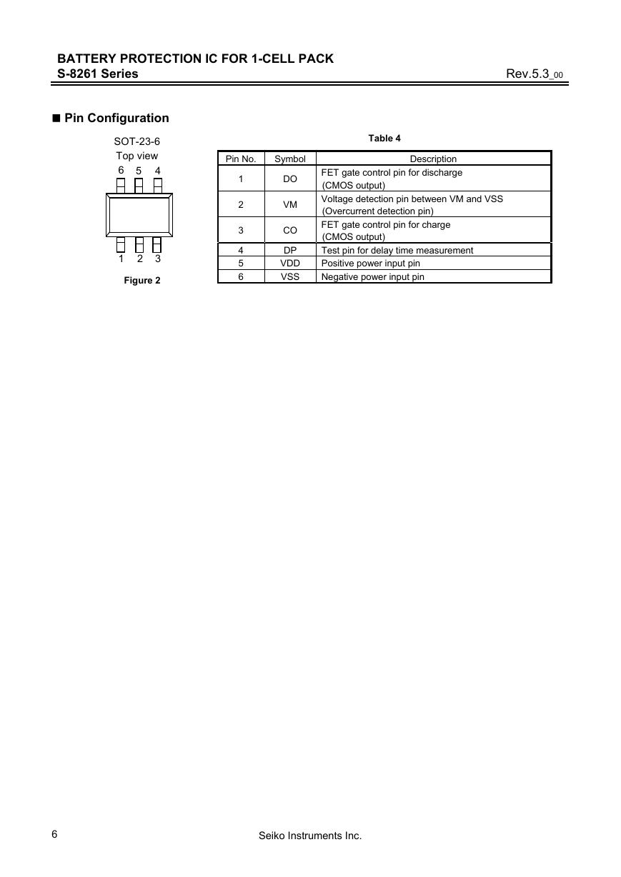
Pin Configuration
SOT-23-6
Top view
6
4
5
1 2 3
Figure 2
Pin No.
Symbol
1
2
3
4
5
6
DO
VM
CO
DP
VDD
VSS
Table 4
Description
FET gate control pin for discharge
(CMOS output)
Voltage detection pin between VM and VSS
(Overcurrent detection pin)
FET gate control pin for charge
(CMOS output)
Test pin for delay time measurement
Positive power input pin
Negative power input pin
6
Seiko Instruments Inc.
�
Rev.5.3_00
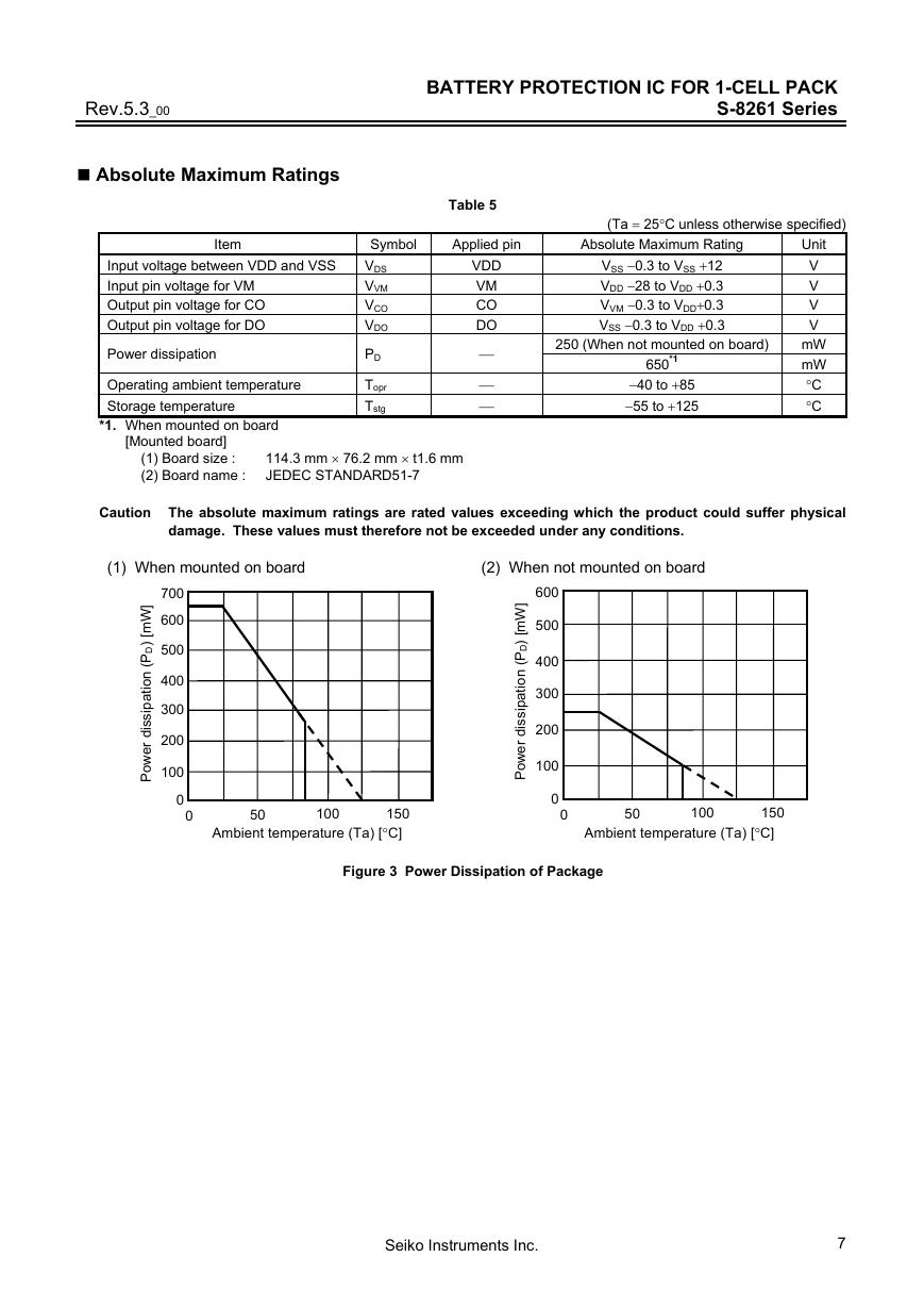
Absolute Maximum Ratings
BATTERY PROTECTION IC FOR 1-CELL PACK
S-8261 Series
Table 5
(Ta = 25°C unless otherwise specified)
Item
Input voltage between VDD and VSS
Input pin voltage for VM
Output pin voltage for CO
Output pin voltage for DO
Power dissipation
Symbol
VDS
VVM
VCO
VDO
PD
Applied pin
Absolute Maximum Rating
VDD
VM
CO
DO
⎯
VSS −0.3 to VSS +12
VDD −28 to VDD +0.3
VVM −0.3 to VDD+0.3
VSS −0.3 to VDD +0.3
250 (When not mounted on board)
650*1
Unit
V
V
V
V
mW
mW
°C
°C
Topr
Tstg
Operating ambient temperature
Storage temperature
*1. When mounted on board
Caution The absolute maximum ratings are rated values exceeding which the product could suffer physical
114.3 mm × 76.2 mm × t1.6 mm
JEDEC STANDARD51-7
[Mounted board]
(1) Board size :
(2) Board name :
−40 to +85
−55 to +125
⎯
⎯
damage. These values must therefore not be exceeded under any conditions.
(1) When mounted on board
(2) When not mounted on board
]
W
m
[
)
D
P
(
n
o
i
t
i
a
p
s
s
d
i
r
e
w
o
P
700
600
500
400
300
200
100
0
0
]
W
m
[
)
D
P
(
n
o
i
t
i
a
p
s
s
d
i
50
150
Ambient temperature (Ta) [°C]
100
r
e
w
o
P
600
500
400
300
200
100
0
0
50
100
150
Ambient temperature (Ta) [°C]
Figure 3 Power Dissipation of Package
Seiko Instruments Inc.
7
�
BATTERY PROTECTION IC FOR 1-CELL PACK
S-8261 Series
Electrical Characteristics
1. Except Detection Delay Time (25°C)
Item
DETECTION VOLTAGE
Overcharge detection voltage
VCU = 3.9 V to 4.5 V, 5 mV Step
Symbol
VCU
Table 6
Condition
⎯
Ta = −5°C to 55°C*1
Rev.5.3_00
(Ta = 25°C unless otherwise specified)
Test
Circuit
Condition
Max.
Typ.
Test
Unit
VCU
VCU
VCU
+0.025
VCU
+0.030
V
V
1
1
1
1
Min.
VCU
−0.025
VCU
−0.030
VHC
−0.025
VDL
−0.050
VHD
−0.050
VIOV1
−0.015
0.4
0.9
−1.0
1.5
1.5
VIOV1
IOPE
IPDN
VHD
VIOV1
1
2
2
3
VHC
VDL
VHD
1
2
2
2
VHC
VDL
VHD
⎯
⎯
⎯
VDL
+0.050
VHC
+0.025
0.5
1.2
−0.7
0.6
1.5
−0.4
V
V
V
V
V
V
V
V
V
⎯
⎯
⎯
⎯
+0.050
VIOV1
+0.015
VIOV2
VSHORT
VCHA
Internal circuit operating voltage
Internal circuit operating voltage
Overcharge hysteresis voltage
VHC = 0.1 V to 0.4 V, 50 mV Step
Overdischarge detection voltage
VDL = 2.0 V to 3.0 V, 10 mV Step
Overdischarge hysteresis voltage
VHD = 0.0 V to 0.7 V, 100 mV Step
Overcurrent 1 detection voltage
VIOV1 = 0.05 V to 0.3 V, 10 mV Step
Overcurrent 2 detection voltage
Load short-circuiting detection voltage
Charger detection voltage
INPUT VOLTAGE, OPERATION VOLTAGE
Operation voltage between VDD and VSS VDSOP1
VDSOP2
Operation voltage between VDD and VM
CURRENT CONSUMPTION (with power-down function)
Current consumption in normal operation
Current consumption at power down
CURRENT CONSUMPTION (without power-down function)
Current consumption in normal operation
Overdischarge current consumption
OUTPUT RESISTANCE
CO pin resistance “H”
CO pin resistance “L”
DO pin resistance “H”
DO pin resistance “L”
VM INTERNAL RESISTANCE
Internal resistance between VM and VDD RVMD
Internal resistance between VM and VSS RVMS
0 V BATTERY CHARGE FUNCTION
0 V battery charge starting charger voltage V0CHA
0 V battery charge inhibition battery voltage V0INH
*1. Since products are not screened at high and low temperatures, the specification for this temperature range is
VDD = 1.8 V, VVM = 0 V
VDD = 3.5 V, VVM = 1.0 V
1.2
0 V battery charge “available”
0 V battery charge “unavailable” ⎯
VCO = 3.0 V, VDD = 3.5 V, VVM = 0 V
VCO = 0.5 V, VDD = 4.5 V, VVM = 0 V
VDO = 3.0 V, VDD = 3.5 V, VVM = 0 V
VDO = 0.5 V, VDD = VVM = 1.8 V
IOPE
IOPED
RCOH
RCOL
RDOH
RDOL
VDD = 3.5 V, VVM = 0 V
VDD = VVM = 1.5 V
VDD = 3.5 V, VVM = 0 V
VDD = VVM = 1.5 V
μA
μA
kΩ
kΩ
kΩ
kΩ
kΩ
kΩ
2
2
4
4
4
4
3
3
2
2
300
20
⎯
⎯
900
40
⎯
0.5
5
5
7
7
8
8
6
6
10
10
10
10
3
3
4
⎯
⎯
2
2
2
⎯
⎯
2.5
2.5
2.5
2.5
1.0
⎯
1.0
1.0
3.5
⎯
3.5
3.0
7.0
0.1
7.0
5.5
100
10
V
V
μA
μA
5
5
5
5
5
5
⎯
⎯
8
28
2
2
11
12
guaranteed by design, not tested in production.
8
Seiko Instruments Inc.
�




 V2版本原理图(Capacitive-Fingerprint-Reader-Schematic_V2).pdf
 摄像头工作原理.doc
 VL53L0X简要说明(En.FLVL53L00216).pdf
 原理图(DVK720-Schematic).pdf
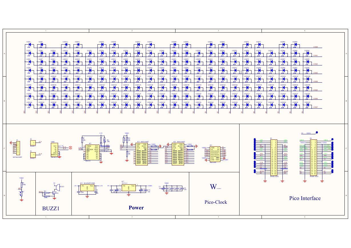 原理图(Pico-Clock-Green-Schdoc).pdf
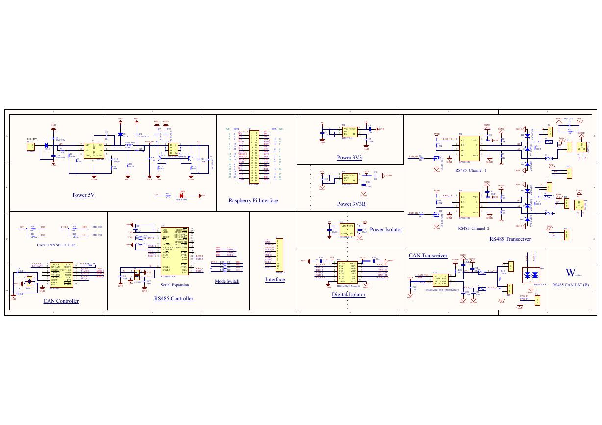 原理图(RS485-CAN-HAT-B-schematic).pdf
 File:SIM7500_SIM7600_SIM7800 Series_SSL_Application Note_V2.00.pdf
 ADS1263(Ads1262).pdf
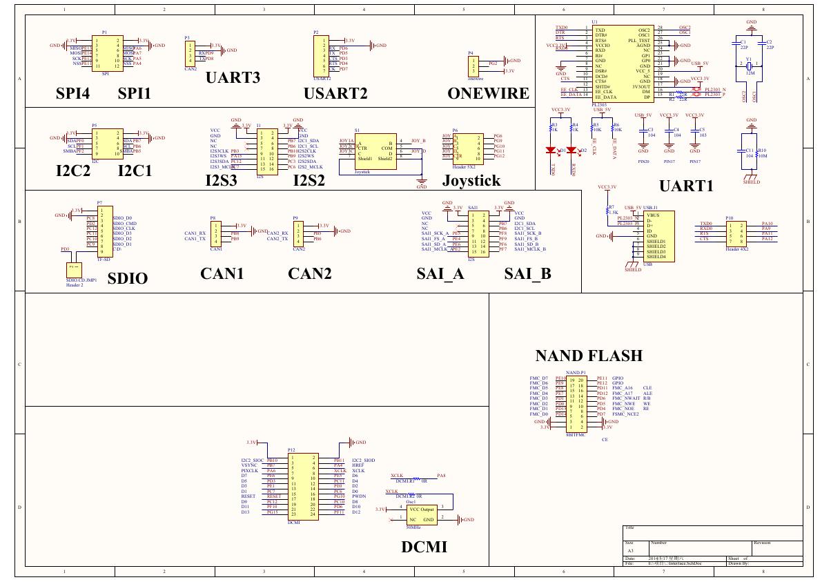 原理图(Open429Z-D-Schematic).pdf
 用户手册(Capacitive_Fingerprint_Reader_User_Manual_CN).pdf
 CY7C68013A(英文版)(CY7C68013A).pdf
 TechnicalReference_Dem.pdf