TPS61088 10-A Fully-Integrated Synchronous Boost Converter
TPS61088
SLVSCM8C –MAY 2015–REVISED FEBRUARY 2019
Input Voltage Range: 2.7 to 12 V
1 Features
1•
• Output Voltage Range: 4.5 to 12.6 V
•
• Up to 91% Efficiency at VIN = 3.3 V, VOUT = 9 V,
10-A Switch Current
and IOUT = 3 A
• Mode Selection Between PFM Mode and Forced
PWM Mode at Light Load
1.0 µA Current into VIN Pin during Shutdown
•
• Resistor-Programmable Switch Peak Current Limit
• Adjustable Switching Frequency: 200 kHz to 2.2
MHz
• Programmable Soft Start
• Output Overvoltage Protection at 13.2 V
• Cycle-by-Cycle Overcurrent Protection
• Thermal Shutdown
•
• Create a Custom Design Using the TPS61088
4.50-mm × 3.50-mm 20-Pin VQFN Package
with the WEBENCH Power Designer
2 Applications
• Portable POS terminal
• Bluetooth™ Speaker
• E-Cigarette
• Thunderbolt Interface
• Quick Charge Power Bank
In moderate to heavy load condition,
3 Description
fully
The TPS61088 is a high power density,
integrated synchronous boost converter with a 11-mΩ
power switch and a 13-mΩ rectifier switch to provide
a high efficiency and small size solution in portable
systems. The TPS61088 has wide input voltage
range from 2.7 V to 12 V to support applications with
single cell or two cell Lithium batteries. The device
has 10-A switch current capability and is capable of
providing an output voltage up to 12.6 V.
The TPS61088 uses adaptive constant off-time peak
topology to regulate the output
current control
voltage.
the
TPS61088 works in the pulse width modulation
(PWM) mode. In light load condition, the device has
two operation modes selected by the MODE pin. One
is the pulse frequency modulation (PFM) mode to
improve the efficiency and another one is the forced
PWM mode to avoid application problems caused by
low switching frequency. The switching frequency in
the PWM mode is adjustable ranging from 200 kHz to
2.2 MHz by an external resistor. The TPS61088 also
implements a programmable soft-start
function and
an adjustable switching peak current limit function. In
addition,
13.2-V output
overvoltage protection, cycle-by-cycle overcurrent
protection, and thermal shutdown protection.
The TPS61088 is available in a 4.50-mm × 3.50-mm
20-pin VQFN package.
provides
device
the
Device Information(1)
PART NUMBER
BODY SIZE (NOM)
TPS61088
4.50 mm × 3.50 mm
(1) For all available packages, see the orderable addendum at
PACKAGE
VQFN (20)
the end of the data sheet.
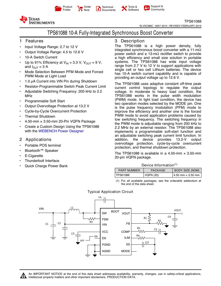
Typical Application Circuit
1
An IMPORTANT NOTICE at the end of this data sheet addresses availability, warranty, changes, use in safety-critical applications,
intellectual property matters and other important disclaimers. PRODUCTION DATA.
VINENVOUTFBR1R5VCCFSWSWR2COMPC5AGNDPGNDC6L1C1C2C3R3BOOTVINILIMR4SSC7C4VOUTMODEONOFFProductFolderOrderNowTechnicalDocumentsTools &SoftwareSupport &Community�
TPS61088
SLVSCM8C –MAY 2015–REVISED FEBRUARY 2019
www.ti.com
Table of Contents
1
Features.................................................................. 1
2 Applications ........................................................... 1
3 Description ............................................................. 1
4 Revision History..................................................... 2
5 Pin Configuration and Functions ......................... 3
6 Specifications......................................................... 4
6.1 Absolute Maximum Ratings ...................................... 4
6.2 ESD Ratings.............................................................. 4
6.3 Recommended Operating Conditions....................... 4
6.4 Thermal Information.................................................. 4
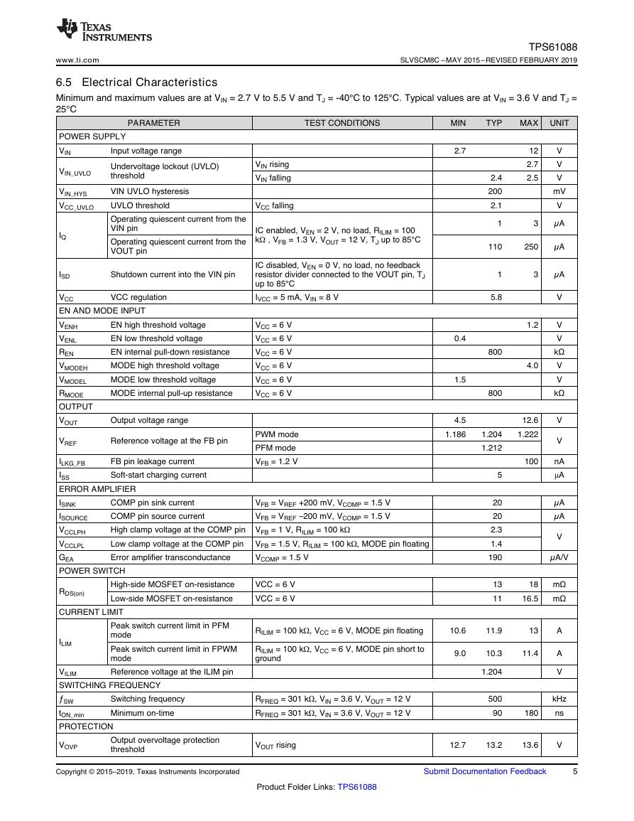
6.5 Electrical Characteristics........................................... 5
6.6 Typical Characteristics.............................................. 6
7 Detailed Description .............................................. 8
7.1 Overview ................................................................... 8
7.2 Functional Block Diagram ......................................... 9
7.3 Feature Description................................................... 9
7.4 Device Functional Modes........................................ 11
8 Application and Implementation ........................ 13
8.1 Application Information............................................ 13
8.2 Typical Application .................................................. 13
9 Power Supply Recommendations...................... 20
10 Layout................................................................... 20
10.1 Layout Guidelines ................................................. 20
10.2 Layout Example .................................................... 20
10.3 Thermal Considerations........................................ 21
11 Device and Documentation Support ................. 22
11.1 Custom Design with WEBENCH Tools................. 22
11.2 Receiving Notification of Documentation Updates 22
11.3 Device Support...................................................... 22
11.4 Community Resources.......................................... 22
11.5 Trademarks ........................................................... 22
11.6 Electrostatic Discharge Caution............................ 22
11.7 Glossary ................................................................ 23
12 Mechanical, Packaging, and Orderable
Information ........................................................... 23
4 Revision History
NOTE: Page numbers for previous revisions may differ from page numbers in the current version.
Changes from Revision B (September) to Revision C
Page
• Corrected spelling of 'resister' to 'resistor' in the Pin Functions table. ................................................................................... 3
• Added caption to Functional Block Diagram as auto-number Figure 10................................................................................ 9
• Added cross-reference hyperlink in the Enable and Startup section pointing to C7 reference in Figure 12. ........................ 9
•
Inserted missing cross-reference hyperlink in Setting Output Voltage section pointing to Figure 12 circuit in the
Typical Application section. .................................................................................................................................................. 14
Changes from Revision A (May 2015) to Revision B
Page
• Added thermal information for EVM configuration ................................................................................................................. 4
Changes from Original (May 2015) to Revision A
Page
• Updated device status to production data ............................................................................................................................. 1
• Updated VCCLPH and VCCLPL typical voltage ............................................................................................................................ 5
•
Fixed legend of Figure 2 and Figure 4 from input to output .................................................................................................. 6
2
Submit Documentation Feedback
Copyright © 2015–2019, Texas Instruments Incorporated
Product Folder Links: TPS61088
�
www.ti.com
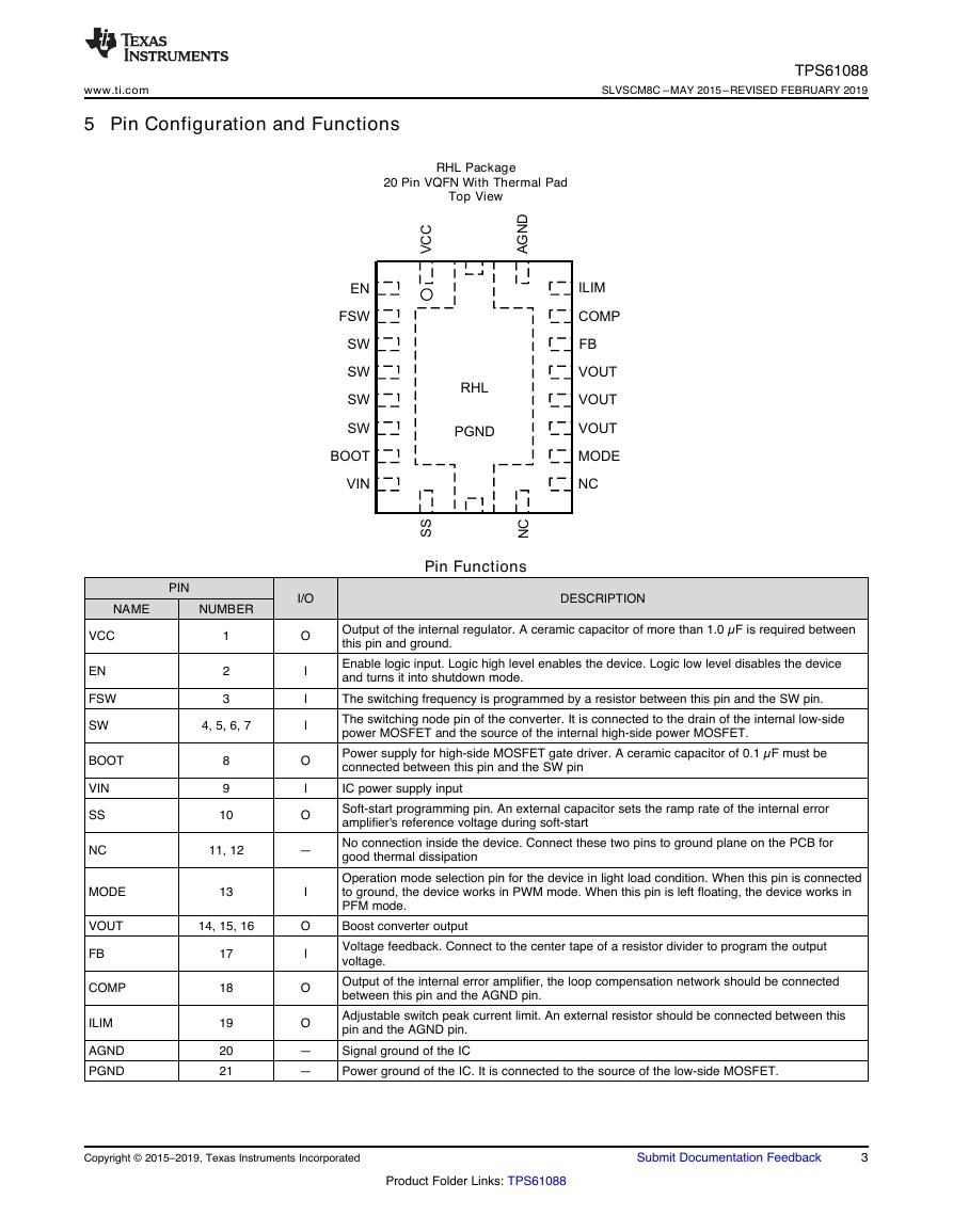
5 Pin Configuration and Functions
TPS61088
SLVSCM8C –MAY 2015–REVISED FEBRUARY 2019
RHL Package
20 Pin VQFN With Thermal Pad
Top View
PIN
NAME
NUMBER
VCC
EN
FSW
SW
BOOT
VIN
SS
NC
MODE
VOUT
FB
COMP
ILIM
AGND
PGND
1
2
3
4, 5, 6, 7
8
9
10
11, 12
13
14, 15, 16
17
18
19
20
21
Pin Functions
DESCRIPTION
Output of the internal regulator. A ceramic capacitor of more than 1.0 µF is required between
this pin and ground.
Enable logic input. Logic high level enables the device. Logic low level disables the device
and turns it into shutdown mode.
The switching frequency is programmed by a resistor between this pin and the SW pin.
The switching node pin of the converter. It is connected to the drain of the internal low-side
power MOSFET and the source of the internal high-side power MOSFET.
Power supply for high-side MOSFET gate driver. A ceramic capacitor of 0.1 µF must be
connected between this pin and the SW pin
IC power supply input
Soft-start programming pin. An external capacitor sets the ramp rate of the internal error
amplifier's reference voltage during soft-start
No connection inside the device. Connect these two pins to ground plane on the PCB for
good thermal dissipation
Operation mode selection pin for the device in light load condition. When this pin is connected
to ground, the device works in PWM mode. When this pin is left floating, the device works in
PFM mode.
Boost converter output
Voltage feedback. Connect to the center tape of a resistor divider to program the output
voltage.
Output of the internal error amplifier, the loop compensation network should be connected
between this pin and the AGND pin.
Adjustable switch peak current limit. An external resistor should be connected between this
pin and the AGND pin.
Signal ground of the IC
Power ground of the IC. It is connected to the source of the low-side MOSFET.
I/O
O
I
I
I
O
I
O
—
I
O
I
O
O
—
—
Copyright © 2015–2019, Texas Instruments Incorporated
Submit Documentation Feedback
3
Product Folder Links: TPS61088
ENSWSWSWBOOTVINFSWSWCOMPFBILIMVOUTVOUTVOUTMODEPGNDVCCRHLNCSSNCAGND�
TPS61088
SLVSCM8C –MAY 2015–REVISED FEBRUARY 2019
6 Specifications
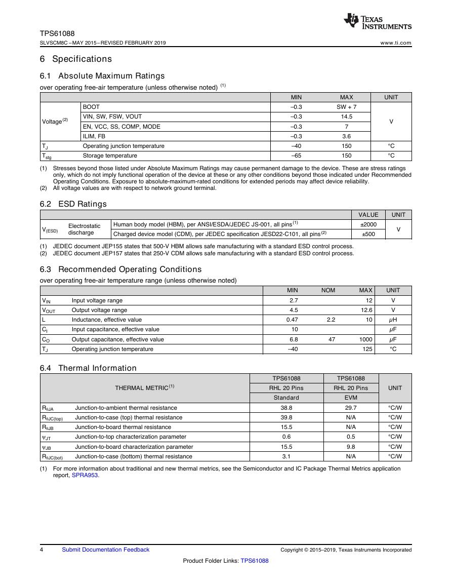
6.1 Absolute Maximum Ratings
over operating free-air temperature (unless otherwise noted) (1)
Voltage(2)
BOOT
VIN, SW, FSW, VOUT
EN, VCC, SS, COMP, MODE
ILIM, FB
Operating junction temperature
Storage temperature
www.ti.com
UNIT
V
MIN
–0.3
–0.3
–0.3
–0.3
–40
–65
MAX
SW + 7
14.5
7
3.6
150
150
TJ
Tstg
(1) Stresses beyond those listed under Absolute Maximum Ratings may cause permanent damage to the device. These are stress ratings
°C
°C
only, which do not imply functional operation of the device at these or any other conditions beyond those indicated under Recommended
Operating Conditions. Exposure to absolute-maximum-rated conditions for extended periods may affect device reliability.
(2) All voltage values are with respect to network ground terminal.
6.2 ESD Ratings
V(ESD)
Electrostatic
discharge
Human body model (HBM), per ANSI/ESDA/JEDEC JS-001, all pins(1)
Charged device model (CDM), per JEDEC specification JESD22-C101, all pins(2)
(1)
(2)
JEDEC document JEP155 states that 500-V HBM allows safe manufacturing with a standard ESD control process.
JEDEC document JEP157 states that 250-V CDM allows safe manufacturing with a standard ESD control process.
VALUE
±2000
±500
UNIT
V
6.3 Recommended Operating Conditions
over operating free-air temperature range (unless otherwise noted)
VIN
VOUT
L
CI
CO
TJ
Input voltage range
Output voltage range
Inductance, effective value
Input capacitance, effective value
Output capacitance, effective value
Operating junction temperature
6.4 Thermal Information
THERMAL METRIC(1)
MIN
2.7
4.5
0.47
10
6.8
–40
NOM
2.2
47
MAX
12
12.6
10
1000
125
UNIT
V
V
µH
µF
µF
°C
TPS61088
RHL 20 Pins
Standard
TPS61088
RHL 20 Pins
UNIT
Junction-to-ambient thermal resistance
Junction-to-case (top) thermal resistance
Junction-to-board thermal resistance
Junction-to-top characterization parameter
Junction-to-board characterization parameter
Junction-to-case (bottom) thermal resistance
RθJA
RθJC(top)
RθJB
ψJT
ψJB
RθJC(bot)
(1) For more information about traditional and new thermal metrics, see the Semiconductor and IC Package Thermal Metrics application
°C/W
°C/W
°C/W
°C/W
°C/W
°C/W
38.8
39.8
15.5
0.6
15.5
3.1
report, SPRA953.
EVM
29.7
N/A
N/A
0.5
9.8
N/A
4
Submit Documentation Feedback
Copyright © 2015–2019, Texas Instruments Incorporated
Product Folder Links: TPS61088
�
www.ti.com
TPS61088
SLVSCM8C –MAY 2015–REVISED FEBRUARY 2019
6.5 Electrical Characteristics
Minimum and maximum values are at VIN = 2.7 V to 5.5 V and TJ = -40°C to 125°C. Typical values are at VIN = 3.6 V and TJ =
25°C
PARAMETER
TEST CONDITIONS
MIN
TYP
MAX UNIT
VIN rising
VIN falling
VCC falling
IC enabled, VEN = 2 V, no load, RILIM = 100
kΩ , VFB = 1.3 V, VOUT = 12 V, TJ up to 85°C
IC disabled, VEN = 0 V, no load, no feedback
resistor divider connected to the VOUT pin, TJ
up to 85°C
IVCC = 5 mA, VIN = 8 V
VCC = 6 V
VCC = 6 V
VCC = 6 V
VCC = 6 V
VCC = 6 V
VCC = 6 V
PWM mode
PFM mode
VFB = 1.2 V
2.7
0.4
1.5
4.5
1.186
POWER SUPPLY
VIN
VIN_UVLO
VIN_HYS
VCC_UVLO
IQ
ISD
Input voltage range
Undervoltage lockout (UVLO)
threshold
VIN UVLO hysteresis
UVLO threshold
Operating quiescent current from the
VIN pin
Operating quiescent current from the
VOUT pin
Shutdown current into the VIN pin
VCC regulation
VCC
EN AND MODE INPUT
VENH
VENL
REN
VMODEH
VMODEL
RMODE
OUTPUT
VOUT
EN high threshold voltage
EN low threshold voltage
EN internal pull-down resistance
MODE high threshold voltage
MODE low threshold voltage
MODE internal pull-up resistance
Output voltage range
VREF
Reference voltage at the FB pin
FB pin leakage current
Soft-start charging current
ILKG_FB
ISS
ERROR AMPLIFIER
ISINK
ISOURCE
VCCLPH
VCCLPL
GEA
POWER SWITCH
12
2.7
2.5
3
250
3
1.2
4.0
12.6
1.222
100
V
V
V
mV
V
µA
µA
µA
V
V
V
kΩ
V
V
kΩ
V
V
nA
μA
µA
µA
V
18
16.5
13
11.4
µA/V
mΩ
mΩ
A
A
V
kHz
ns
180
2.4
200
2.1
1
110
1
5.8
800
800
1.204
1.212
5
20
20
2.3
1.4
190
13
11
11.9
10.3
1.204
500
90
COMP pin sink current
COMP pin source current
High clamp voltage at the COMP pin VFB = 1 V, RILIM = 100 kΩ
Low clamp voltage at the COMP pin
Error amplifier transconductance
VFB = VREF +200 mV, VCOMP = 1.5 V
VFB = VREF –200 mV, VCOMP = 1.5 V
VFB = 1.5 V, RILIM = 100 kΩ, MODE pin floating
VCOMP = 1.5 V
RDS(on)
High-side MOSFET on-resistance
Low-side MOSFET on-resistance
VCC = 6 V
VCC = 6 V
CURRENT LIMIT
ILIM
Peak switch current limit in PFM
mode
Peak switch current limit in FPWM
mode
Reference voltage at the ILIM pin
VILIM
SWITCHING FREQUENCY
ƒSW
tON_min
PROTECTION
Switching frequency
Minimum on-time
RILIM = 100 kΩ, VCC = 6 V, MODE pin floating
RILIM = 100 kΩ, VCC = 6 V, MODE pin short to
ground
10.6
9.0
RFREQ = 301 kΩ, VIN = 3.6 V, VOUT = 12 V
RFREQ = 301 kΩ, VIN = 3.6 V, VOUT = 12 V
VOVP
Output overvoltage protection
threshold
VOUT rising
12.7
13.2
13.6
V
Copyright © 2015–2019, Texas Instruments Incorporated
Submit Documentation Feedback
5
Product Folder Links: TPS61088
�
TPS61088
SLVSCM8C –MAY 2015–REVISED FEBRUARY 2019
www.ti.com
Electrical Characteristics (continued)
Minimum and maximum values are at VIN = 2.7 V to 5.5 V and TJ = -40°C to 125°C. Typical values are at VIN = 3.6 V and TJ =
25°C
PARAMETER
TEST CONDITIONS
MIN
Output overvoltage protection
VOVP_HYS
hysteresis
THERMAL SHUTDOWN
TSD
TSD_HYS
Thermal shutdown threshold
Thermal shutdown hysteresis
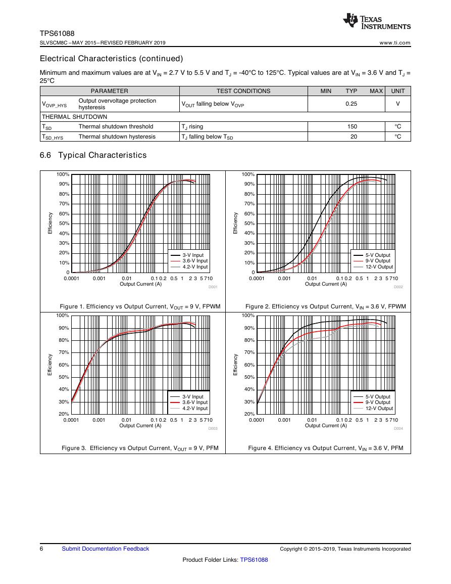
6.6 Typical Characteristics
VOUT falling below VOVP
TJ rising
TJ falling below TSD
TYP
0.25
150
20
MAX UNIT
V
°C
°C
Figure 1. Efficiency vs Output Current, VOUT = 9 V, FPWM
Figure 2. Efficiency vs Output Current, VIN = 3.6 V, FPWM
Figure 3. Efficiency vs Output Current, VOUT = 9 V, PFM
Figure 4. Efficiency vs Output Current, VIN = 3.6 V, PFM
6
Submit Documentation Feedback
Copyright © 2015–2019, Texas Instruments Incorporated
Product Folder Links: TPS61088
Output Current (A)Efficiency0.00010.0010.010.10.20.5123571020%30%40%50%60%70%80%90%100%D0033-V Input3.6-V Input4.2-V InputOutput Current (A)Efficiency0.00010.0010.010.10.20.5123571020%30%40%50%60%70%80%90%100%D0045-V Output9-V Output12-V OutputOutput Current (A)Efficiency0.00010.0010.010.10.20.51235710010%20%30%40%50%60%70%80%90%100%D0013-V Input3.6-V Input4.2-V InputOutput Current (A)Efficiency0.00010.0010.010.10.20.51235710010%20%30%40%50%60%70%80%90%100%D0025-V Output9-V Output12-V Output�
www.ti.com
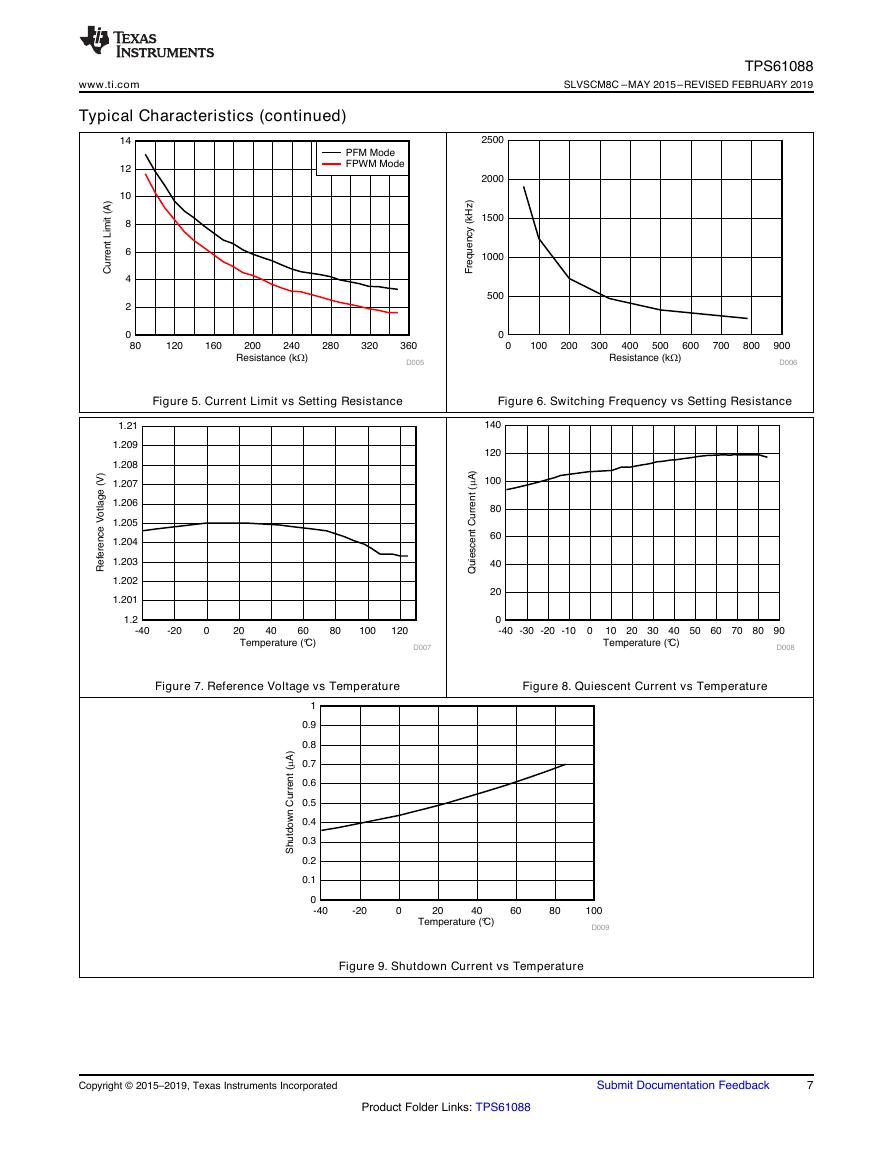
Typical Characteristics (continued)
TPS61088
SLVSCM8C –MAY 2015–REVISED FEBRUARY 2019
Figure 5. Current Limit vs Setting Resistance
Figure 6. Switching Frequency vs Setting Resistance
Figure 7. Reference Voltage vs Temperature
Figure 8. Quiescent Current vs Temperature
Figure 9. Shutdown Current vs Temperature
Copyright © 2015–2019, Texas Instruments Incorporated
Submit Documentation Feedback
7
Product Folder Links: TPS61088
Temperature (°C)Shutdown Current (PA)-40-2002040608010000.10.20.30.40.50.60.70.80.91D009Temperature (°C)Reference Votlage (V)-40-200204060801001201301.21.2011.2021.2031.2041.2051.2061.2071.2081.2091.21D007 Temperature (°C)Quiescent Current (PA)-40-30-20-100102030405060708090020406080100120140D008Resistance (k:)Current Limit (A)8012016020024028032036002468101214D005PFM ModeFPWM ModeResistance (k:)Frequency (kHz)010020030040050060070080090005001000150020002500D006�
TPS61088
SLVSCM8C –MAY 2015–REVISED FEBRUARY 2019
7 Detailed Description
www.ti.com
7.1 Overview
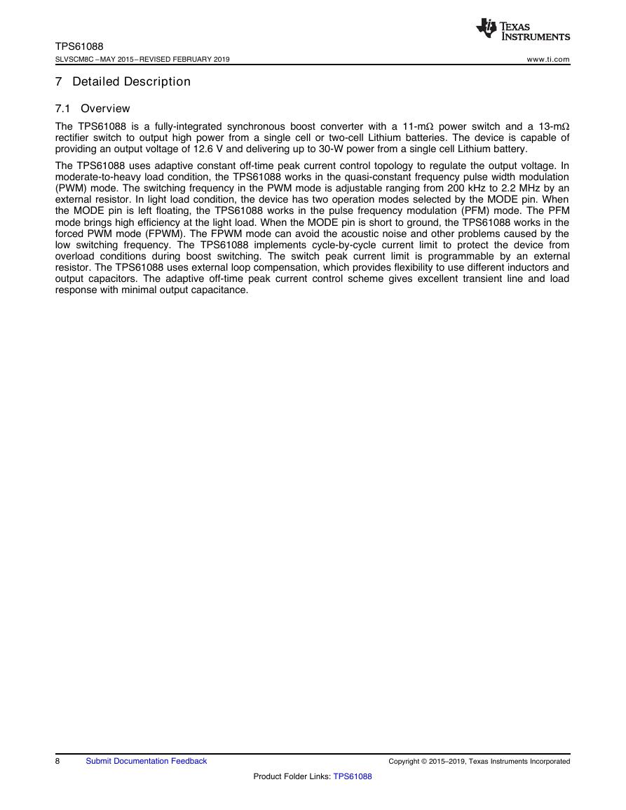
The TPS61088 is a fully-integrated synchronous boost converter with a 11-mΩ power switch and a 13-mΩ
rectifier switch to output high power from a single cell or two-cell Lithium batteries. The device is capable of
providing an output voltage of 12.6 V and delivering up to 30-W power from a single cell Lithium battery.
The TPS61088 uses adaptive constant off-time peak current control topology to regulate the output voltage. In
moderate-to-heavy load condition, the TPS61088 works in the quasi-constant frequency pulse width modulation
(PWM) mode. The switching frequency in the PWM mode is adjustable ranging from 200 kHz to 2.2 MHz by an
external resistor. In light load condition, the device has two operation modes selected by the MODE pin. When
the MODE pin is left floating, the TPS61088 works in the pulse frequency modulation (PFM) mode. The PFM
mode brings high efficiency at the light load. When the MODE pin is short to ground, the TPS61088 works in the
forced PWM mode (FPWM). The FPWM mode can avoid the acoustic noise and other problems caused by the
low switching frequency. The TPS61088 implements cycle-by-cycle current limit to protect the device from
overload conditions during boost switching. The switch peak current
is programmable by an external
resistor. The TPS61088 uses external loop compensation, which provides flexibility to use different inductors and
output capacitors. The adaptive off-time peak current control scheme gives excellent transient line and load
response with minimal output capacitance.
limit
8
Submit Documentation Feedback
Copyright © 2015–2019, Texas Instruments Incorporated
Product Folder Links: TPS61088
�


 V2版本原理图(Capacitive-Fingerprint-Reader-Schematic_V2).pdf
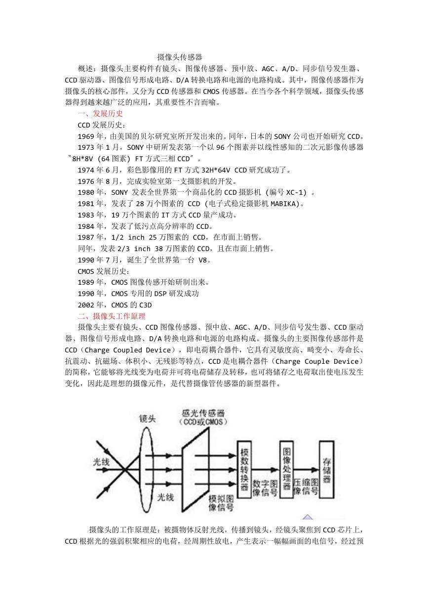 摄像头工作原理.doc
 VL53L0X简要说明(En.FLVL53L00216).pdf
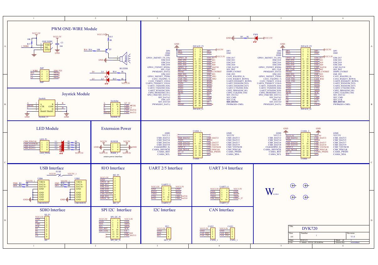 原理图(DVK720-Schematic).pdf
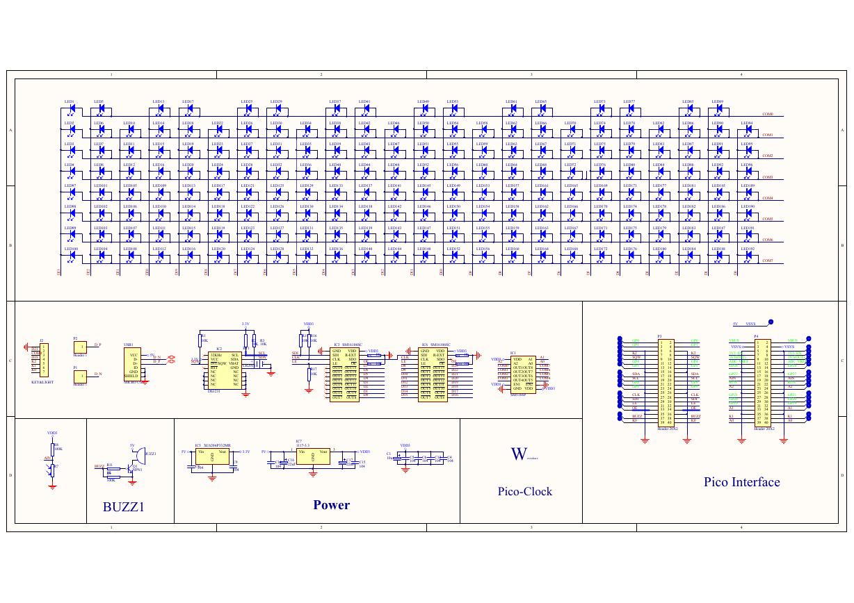 原理图(Pico-Clock-Green-Schdoc).pdf
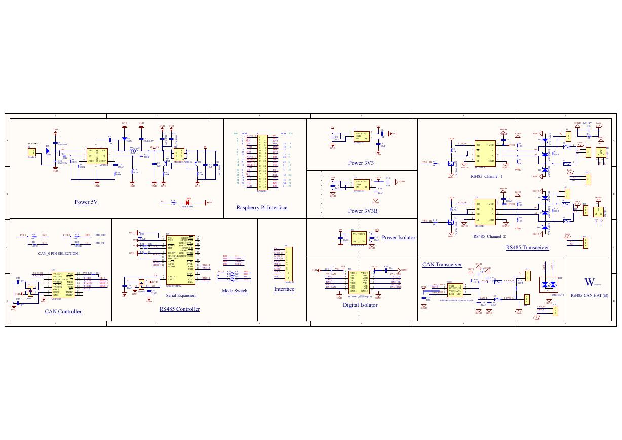 原理图(RS485-CAN-HAT-B-schematic).pdf
 File:SIM7500_SIM7600_SIM7800 Series_SSL_Application Note_V2.00.pdf
 ADS1263(Ads1262).pdf
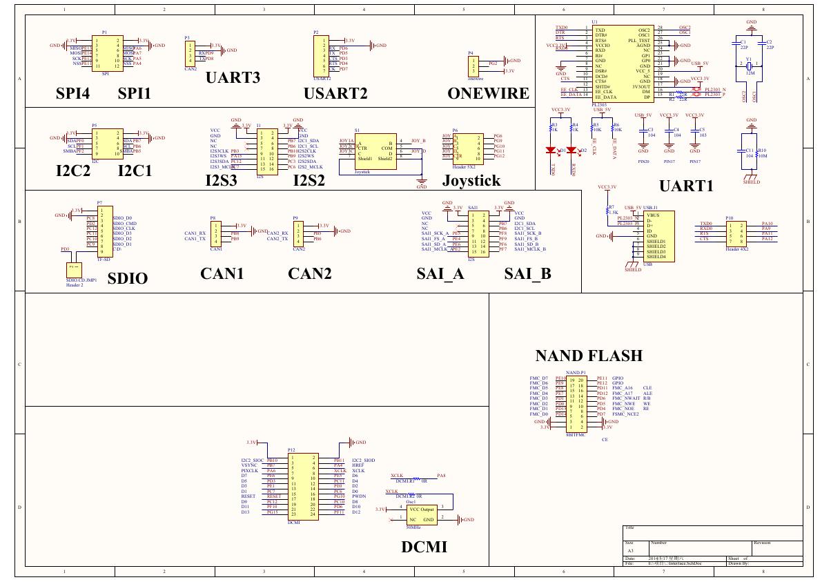 原理图(Open429Z-D-Schematic).pdf
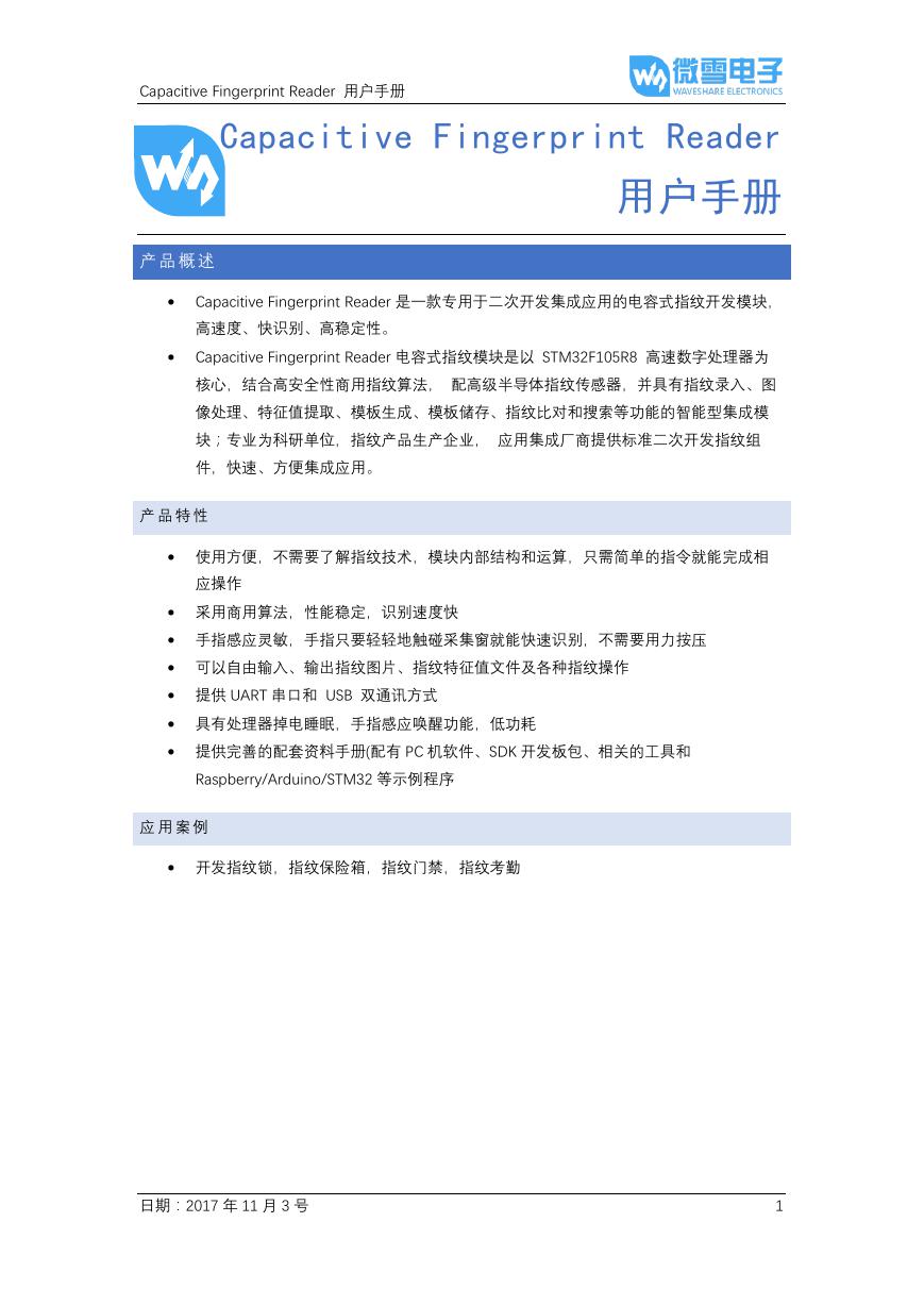 用户手册(Capacitive_Fingerprint_Reader_User_Manual_CN).pdf
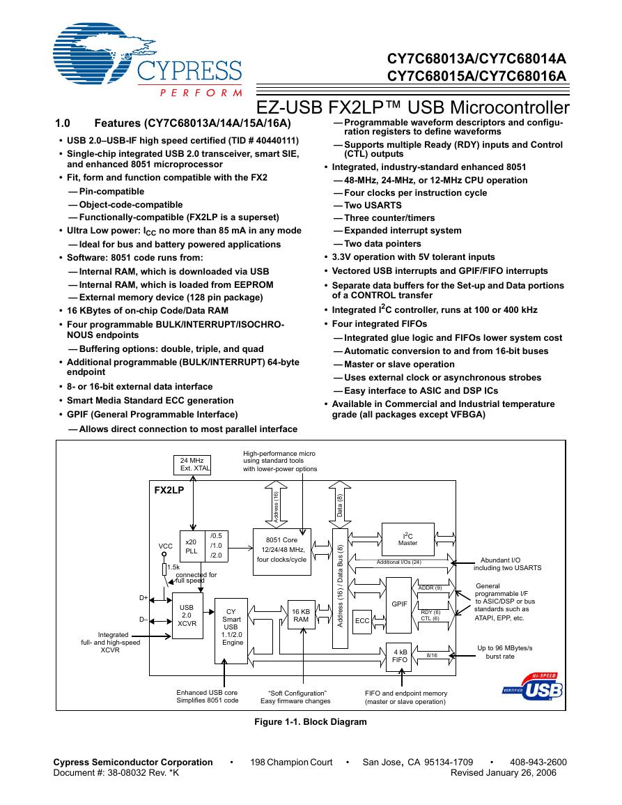 CY7C68013A(英文版)(CY7C68013A).pdf
 TechnicalReference_Dem.pdf