logo资料库

STM32 Cortex-M3编程手册.pdf

第1页 / 共156页
第2页 / 共156页
第3页 / 共156页
第4页 / 共156页
第5页 / 共156页
第6页 / 共156页
第7页 / 共156页
第8页 / 共156页
资料共156页,剩余部分请下载后查看
1 About this document
1.1 Typographical conventions
1.2 List of abbreviations for registers
1.3 About the STM32 Cortex®-M3 processor and core peripherals
Figure 1. STM32 Cortex-M3 implementation
1.3.1 System level interface
1.3.2 Integrated configurable debug
1.3.3 Cortex®-M3 processor features and benefits summary
1.3.4 Cortex®-M3 core peripherals
2 The Cortex®-M3 processor
2.1 Programmers model
2.1.1 Processor mode and privilege levels for software execution
2.1.2 Stacks
Table 1. Summary of processor mode, execution privilege level, and stack use options
2.1.3 Core registers
Figure 2. Processor core registers
Table 2. Core register set summary
Figure 3. APSR, IPSR and EPSR bit assignments
Figure 4. PSR bit assignments
Table 3. PSR register combinations
Table 4. APSR bit definitions
Table 5. IPSR bit definitions
Table 6. EPSR bit definitions
Figure 5. PRIMASK bit assignments
Table 7. PRIMASK register bit definitions
Figure 6. FAULTMASK bit assignments
Table 8. FAULTMASK register bit definitions
Figure 7. BASEPRI bit assignments
Table 9. BASEPRI register bit assignments
Figure 8. CONTROL bit assignments
Table 10. CONTROL register bit definitions
2.1.4 Exceptions and interrupts
2.1.5 Data types
2.1.6 The Cortex® microcontroller software interface standard (CMSIS)
2.2 Memory model
Figure 9. Memory map
2.2.1 Memory regions, types and attributes
2.2.2 Memory system ordering of memory accesses
Table 11. Ordering of memory accesses
2.2.3 Behavior of memory accesses
Table 12. Memory access behavior
2.2.4 Software ordering of memory accesses
2.2.5 Bit-banding
Table 13. SRAM memory bit-banding regions
Table 14. Peripheral memory bit-banding regions
Figure 10. Bit-band mapping
2.2.6 Memory endianness
Figure 11. Little-endian example
2.2.7 Synchronization primitives
2.2.8 Programming hints for the synchronization primitives
Table 15. C compiler intrinsic functions for exclusive access instructions
2.3 Exception model
2.3.1 Exception states
2.3.2 Exception types
Table 16. Properties of the different exception types
2.3.3 Exception handlers
2.3.4 Vector table
Figure 12. Vector table
2.3.5 Exception priorities
2.3.6 Interrupt priority grouping
2.3.7 Exception entry and return
Table 17. Exception return behavior
2.4 Fault handling
2.4.1 Fault types
Table 18. Faults
2.4.2 Fault escalation and hard faults
2.4.3 Fault status registers and fault address registers
Table 19. Fault status and fault address registers
2.4.4 Lockup
2.5 Power management
2.5.1 Entering sleep mode
2.5.2 Wakeup from sleep mode
2.5.3 The external event input
2.5.4 Power management programming hints
3 The Cortex®-M3 instruction set
3.1 Instruction set summary
Table 20. Cortex-M3 instructions
3.2 Intrinsic functions
Table 21. CMSIS intrinsic functions to generate some Cortex-M3 instructions
Table 22. CMSIS intrinsic functions to access the special registers
3.3 About the instruction descriptions
3.3.1 Operands
3.3.2 Restrictions when using PC or SP
3.3.3 Flexible second operand
3.3.4 Shift operations
Figure 13. ASR#3
Figure 14. LSR#3
Figure 15. LSL#3
Figure 16. ROR #3
Figure 17. RRX #3
3.3.5 Address alignment
3.3.6 PC-relative expressions
3.3.7 Conditional execution
Table 23. Condition code suffixes
3.3.8 Instruction width selection
3.4 Memory access instructions
Table 24. Memory access instructions
3.4.1 ADR
3.4.2 LDR and STR, immediate offset
Table 25. Immediate, pre-indexed and post-indexed offset ranges
3.4.3 LDR and STR, register offset
3.4.4 LDR and STR, unprivileged
3.4.5 LDR, PC-relative
Table 26. label-PC offset ranges
3.4.6 LDM and STM
3.4.7 PUSH and POP
3.4.8 LDREX and STREX
3.4.9 CLREX
3.5 General data processing instructions
Table 27. Data processing instructions
3.5.1 ADD, ADC, SUB, SBC, and RSB
3.5.2 AND, ORR, EOR, BIC, and ORN
3.5.3 ASR, LSL, LSR, ROR, and RRX
3.5.4 CLZ
3.5.5 CMP and CMN
3.5.6 MOV and MVN
3.5.7 MOVT
3.5.8 REV, REV16, REVSH, and RBIT
3.5.9 TST and TEQ
3.6 Multiply and divide instructions
Table 28. Multiply and divide instructions
3.6.1 MUL, MLA, and MLS
3.6.2 UMULL, UMLAL, SMULL, and SMLAL
3.6.3 SDIV and UDIV
3.7 Saturating instructions
3.7.1 SSAT and USAT
3.8 Bitfield instructions
Table 29. Packing and unpacking instructions
3.8.1 BFC and BFI
3.8.2 SBFX and UBFX
3.8.3 SXT and UXT
3.8.4 Branch and control instructions
Table 30. Branch and control instructions
3.8.5 B, BL, BX, and BLX
Table 31. Branch ranges
3.8.6 CBZ and CBNZ
3.8.7 IT
3.8.8 TBB and TBH
3.9 Miscellaneous instructions
Table 32. Miscellaneous instructions
3.9.1 BKPT
3.9.2 CPS
3.9.3 DMB
3.9.4 DSB
3.9.5 ISB
3.9.6 MRS
3.9.7 MSR
3.9.8 NOP
3.9.9 SEV
3.9.10 SVC
3.9.11 WFE
3.9.12 WFI
4 Core peripherals
4.1 About the STM32 core peripherals
Table 33. STM32 core peripheral register regions
4.2 Memory protection unit (MPU)
Table 34. Memory attributes summary
4.2.1 MPU access permission attributes
Table 35. TEX, C, B, and S encoding
Table 36. Cache policy for memory attribute encoding
Table 37. AP encoding
4.2.2 MPU mismatch
4.2.3 Updating an MPU region
Figure 18. Subregion example
4.2.4 MPU design hints and tips
Table 38. Memory region attributes for STM32
4.2.5 MPU type register (MPU_TYPER)
4.2.6 MPU control register (MPU_CR)
4.2.7 MPU region number register (MPU_RNR)
4.2.8 MPU region base address register (MPU_RBAR)
4.2.9 MPU region attribute and size register (MPU_RASR)
Table 39. Example SIZE field values
Table 40. MPU register map and reset values
4.3 Nested vectored interrupt controller (NVIC)
4.3.1 The CMSIS mapping of the Cortex®-M3 NVIC registers
Table 41. Mapping of interrupts to the interrupt variables
4.3.2 Interrupt set-enable registers (NVIC_ISERx)
4.3.3 Interrupt clear-enable registers (NVIC_ICERx)
4.3.4 Interrupt set-pending registers (NVIC_ISPRx)
4.3.5 Interrupt clear-pending registers (NVIC_ICPRx)
4.3.6 Interrupt active bit registers (NVIC_IABRx)
4.3.7 Interrupt priority registers (NVIC_IPRx)
Figure 19. NVIC_IPRx register mapping
Table 42. IPR bit assignments
4.3.8 Software trigger interrupt register (NVIC_STIR)
4.3.9 Level-sensitive and pulse interrupts
4.3.10 NVIC design hints and tips
Table 43. CMSIS functions for NVIC control
4.3.11 NVIC register map
Table 44. NVIC register map and reset values
4.4 System control block (SCB)
4.4.1 Auxiliary control register (SCB_ACTLR)
4.4.2 CPUID base register (SCB_CPUID)
4.4.3 Interrupt control and state register (SCB_ICSR)
4.4.4 Vector table offset register (SCB_VTOR)
4.4.5 Application interrupt and reset control register (SCB_AIRCR)
Table 45. Priority grouping
4.4.6 System control register (SCB_SCR)
4.4.7 Configuration and control register (SCB_CCR)
4.4.8 System handler priority registers (SHPRx)
Table 46. System fault handler priority fields
4.4.9 System handler control and state register (SCB_SHCSR)
4.4.10 Configurable fault status register (SCB_CFSR)
Figure 20. CFSR subregisters
4.4.11 Hard fault status register (SCB_HFSR)
4.4.12 Memory management fault address register (SCB_MMFAR)
4.4.13 Bus fault address register (SCB_BFAR)
4.4.14 System control block design hints and tips
4.4.15 SCB register map
Table 47. SCB register map and reset value for STM32F2 and STM32L
Table 48. SCB register map and reset values
4.5 SysTick timer (STK)
4.5.1 SysTick control and status register (STK_CTRL)
4.5.2 SysTick reload value register (STK_LOAD)
4.5.3 SysTick current value register (STK_VAL)
4.5.4 SysTick calibration value register (STK_CALIB)
4.5.5 SysTick design hints and tips
4.5.6 SysTick register map
Table 49. SysTick register map and reset values
5 Revision history
Table 50. Document revision history
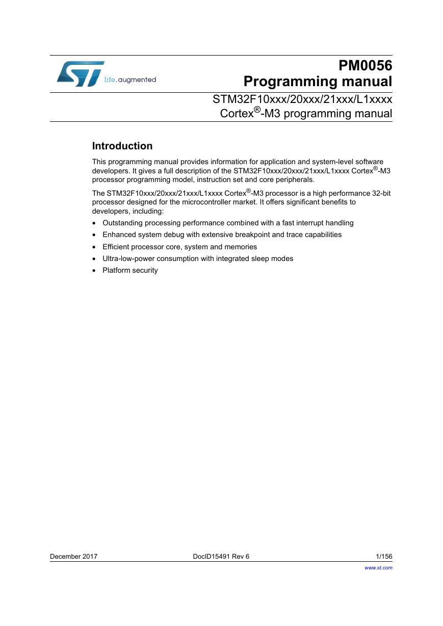
PM0056 Programming manual STM32F10xxx/20xxx/21xxx/L1xxxx Cortex®-M3 programming manual Introduction This programming manual provides information for application and system-level software developers. It gives a full description of the STM32F10xxx/20xxx/21xxx/L1xxxx Cortex®-M3 processor programming model, instruction set and core peripherals. The STM32F10xxx/20xxx/21xxx/L1xxxx Cortex®-M3 processor is a high performance 32-bit processor designed for the microcontroller market. It offers significant benefits to developers, including: • Outstanding processing performance combined with a fast interrupt handling • Enhanced system debug with extensive breakpoint and trace capabilities • Efficient processor core, system and memories • Ultra-low-power consumption with integrated sleep modes • Platform security December 2017 DocID15491 Rev 6 1/156 www.st.com 1
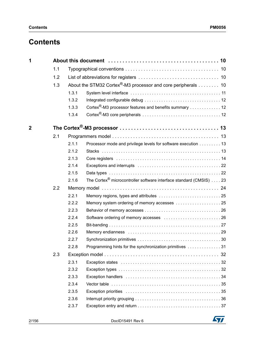
Contents Contents PM0056 1 2 About this document . . . . . . . . . . . . . . . . . . . . . . . . . . . . . . . . . . . . . . . 10 Typographical conventions . . . . . . . . . . . . . . . . . . . . . . . . . . . . . . . . . . . . 10 1.1 1.2 List of abbreviations for registers . . . . . . . . . . . . . . . . . . . . . . . . . . . . . . . 10 About the STM32 Cortex®-M3 processor and core peripherals . . . . . . . . 10 1.3 System level interface . . . . . . . . . . . . . . . . . . . . . . . . . . . . . . . . . . . . . . 11 1.3.1 1.3.2 Integrated configurable debug . . . . . . . . . . . . . . . . . . . . . . . . . . . . . . . . 12 Cortex®-M3 processor features and benefits summary . . . . . . . . . . . . . 12 1.3.3 Cortex®-M3 core peripherals . . . . . . . . . . . . . . . . . . . . . . . . . . . . . . . . . 12 1.3.4 2.2 The Cortex®-M3 processor . . . . . . . . . . . . . . . . . . . . . . . . . . . . . . . . . . . 13 Programmers model . . . . . . . . . . . . . . . . . . . . . . . . . . . . . . . . . . . . . . . . . 13 2.1 2.1.1 Processor mode and privilege levels for software execution . . . . . . . . . 13 Stacks . . . . . . . . . . . . . . . . . . . . . . . . . . . . . . . . . . . . . . . . . . . . . . . . . . 13 2.1.2 2.1.3 Core registers . . . . . . . . . . . . . . . . . . . . . . . . . . . . . . . . . . . . . . . . . . . . 14 Exceptions and interrupts . . . . . . . . . . . . . . . . . . . . . . . . . . . . . . . . . . . 22 2.1.4 Data types . . . . . . . . . . . . . . . . . . . . . . . . . . . . . . . . . . . . . . . . . . . . . . . 22 2.1.5 The Cortex® microcontroller software interface standard (CMSIS) . . . . 23 2.1.6 Memory model . . . . . . . . . . . . . . . . . . . . . . . . . . . . . . . . . . . . . . . . . . . . . 24 Memory regions, types and attributes . . . . . . . . . . . . . . . . . . . . . . . . . . 25 2.2.1 2.2.2 Memory system ordering of memory accesses . . . . . . . . . . . . . . . . . . . 25 Behavior of memory accesses . . . . . . . . . . . . . . . . . . . . . . . . . . . . . . . . 26 2.2.3 Software ordering of memory accesses . . . . . . . . . . . . . . . . . . . . . . . . 26 2.2.4 2.2.5 Bit-banding . . . . . . . . . . . . . . . . . . . . . . . . . . . . . . . . . . . . . . . . . . . . . . . 27 Memory endianness . . . . . . . . . . . . . . . . . . . . . . . . . . . . . . . . . . . . . . . 29 2.2.6 Synchronization primitives . . . . . . . . . . . . . . . . . . . . . . . . . . . . . . . . . . . 30 2.2.7 2.2.8 Programming hints for the synchronization primitives . . . . . . . . . . . . . . 31 Exception model . . . . . . . . . . . . . . . . . . . . . . . . . . . . . . . . . . . . . . . . . . . . 32 Exception states . . . . . . . . . . . . . . . . . . . . . . . . . . . . . . . . . . . . . . . . . . 32 2.3.1 2.3.2 Exception types . . . . . . . . . . . . . . . . . . . . . . . . . . . . . . . . . . . . . . . . . . . 32 Exception handlers . . . . . . . . . . . . . . . . . . . . . . . . . . . . . . . . . . . . . . . . 34 2.3.3 Vector table . . . . . . . . . . . . . . . . . . . . . . . . . . . . . . . . . . . . . . . . . . . . . . 35 2.3.4 2.3.5 Exception priorities . . . . . . . . . . . . . . . . . . . . . . . . . . . . . . . . . . . . . . . . 35 Interrupt priority grouping . . . . . . . . . . . . . . . . . . . . . . . . . . . . . . . . . . . . 36 2.3.6 2.3.7 Exception entry and return . . . . . . . . . . . . . . . . . . . . . . . . . . . . . . . . . . . 37 2.3 2/156 DocID15491 Rev 6
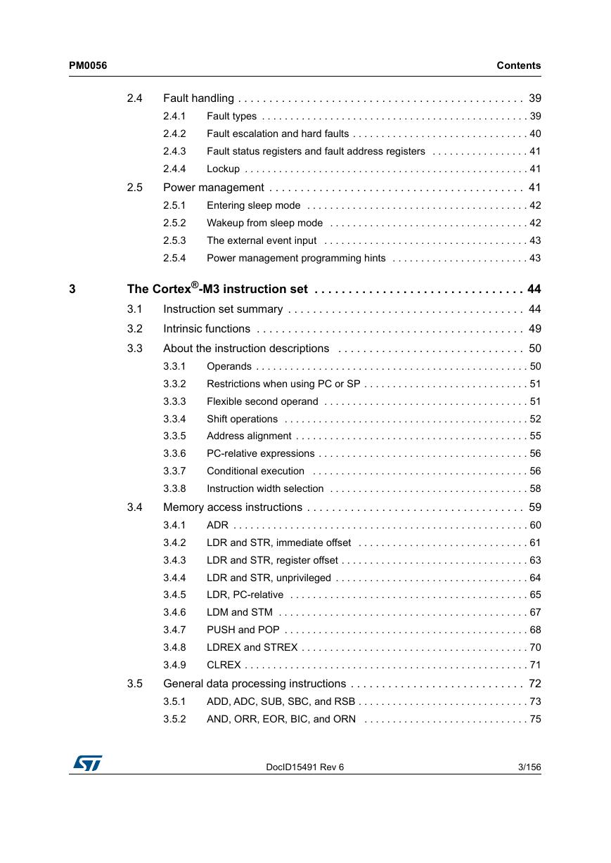
PM0056 Contents 2.4 2.5 Fault handling . . . . . . . . . . . . . . . . . . . . . . . . . . . . . . . . . . . . . . . . . . . . . . 39 Fault types . . . . . . . . . . . . . . . . . . . . . . . . . . . . . . . . . . . . . . . . . . . . . . . 39 2.4.1 2.4.2 Fault escalation and hard faults . . . . . . . . . . . . . . . . . . . . . . . . . . . . . . . 40 Fault status registers and fault address registers . . . . . . . . . . . . . . . . . 41 2.4.3 2.4.4 Lockup . . . . . . . . . . . . . . . . . . . . . . . . . . . . . . . . . . . . . . . . . . . . . . . . . . 41 Power management . . . . . . . . . . . . . . . . . . . . . . . . . . . . . . . . . . . . . . . . . 41 Entering sleep mode . . . . . . . . . . . . . . . . . . . . . . . . . . . . . . . . . . . . . . . 42 2.5.1 Wakeup from sleep mode . . . . . . . . . . . . . . . . . . . . . . . . . . . . . . . . . . . 42 2.5.2 2.5.3 The external event input . . . . . . . . . . . . . . . . . . . . . . . . . . . . . . . . . . . . 43 Power management programming hints . . . . . . . . . . . . . . . . . . . . . . . . 43 2.5.4 3 The Cortex®-M3 instruction set . . . . . . . . . . . . . . . . . . . . . . . . . . . . . . . 44 Instruction set summary . . . . . . . . . . . . . . . . . . . . . . . . . . . . . . . . . . . . . . 44 3.1 3.2 Intrinsic functions . . . . . . . . . . . . . . . . . . . . . . . . . . . . . . . . . . . . . . . . . . . 49 About the instruction descriptions . . . . . . . . . . . . . . . . . . . . . . . . . . . . . . 50 3.3 Operands . . . . . . . . . . . . . . . . . . . . . . . . . . . . . . . . . . . . . . . . . . . . . . . . 50 3.3.1 3.3.2 Restrictions when using PC or SP . . . . . . . . . . . . . . . . . . . . . . . . . . . . . 51 Flexible second operand . . . . . . . . . . . . . . . . . . . . . . . . . . . . . . . . . . . . 51 3.3.3 Shift operations . . . . . . . . . . . . . . . . . . . . . . . . . . . . . . . . . . . . . . . . . . . 52 3.3.4 3.3.5 Address alignment . . . . . . . . . . . . . . . . . . . . . . . . . . . . . . . . . . . . . . . . . 55 PC-relative expressions . . . . . . . . . . . . . . . . . . . . . . . . . . . . . . . . . . . . . 56 3.3.6 Conditional execution . . . . . . . . . . . . . . . . . . . . . . . . . . . . . . . . . . . . . . 56 3.3.7 3.3.8 Instruction width selection . . . . . . . . . . . . . . . . . . . . . . . . . . . . . . . . . . . 58 Memory access instructions . . . . . . . . . . . . . . . . . . . . . . . . . . . . . . . . . . . 59 ADR . . . . . . . . . . . . . . . . . . . . . . . . . . . . . . . . . . . . . . . . . . . . . . . . . . . . 60 3.4.1 3.4.2 LDR and STR, immediate offset . . . . . . . . . . . . . . . . . . . . . . . . . . . . . . 61 LDR and STR, register offset . . . . . . . . . . . . . . . . . . . . . . . . . . . . . . . . . 63 3.4.3 LDR and STR, unprivileged . . . . . . . . . . . . . . . . . . . . . . . . . . . . . . . . . . 64 3.4.4 3.4.5 LDR, PC-relative . . . . . . . . . . . . . . . . . . . . . . . . . . . . . . . . . . . . . . . . . . 65 LDM and STM . . . . . . . . . . . . . . . . . . . . . . . . . . . . . . . . . . . . . . . . . . . . 67 3.4.6 PUSH and POP . . . . . . . . . . . . . . . . . . . . . . . . . . . . . . . . . . . . . . . . . . . 68 3.4.7 3.4.8 LDREX and STREX . . . . . . . . . . . . . . . . . . . . . . . . . . . . . . . . . . . . . . . . 70 3.4.9 CLREX . . . . . . . . . . . . . . . . . . . . . . . . . . . . . . . . . . . . . . . . . . . . . . . . . . 71 General data processing instructions . . . . . . . . . . . . . . . . . . . . . . . . . . . . 72 3.5.1 ADD, ADC, SUB, SBC, and RSB . . . . . . . . . . . . . . . . . . . . . . . . . . . . . . 73 AND, ORR, EOR, BIC, and ORN . . . . . . . . . . . . . . . . . . . . . . . . . . . . . 75 3.5.2 3.4 3.5 DocID15491 Rev 6 3/156 6
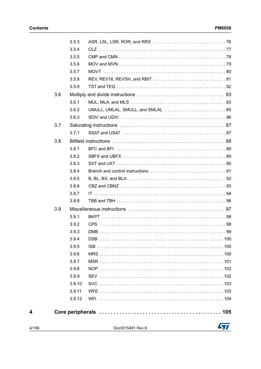
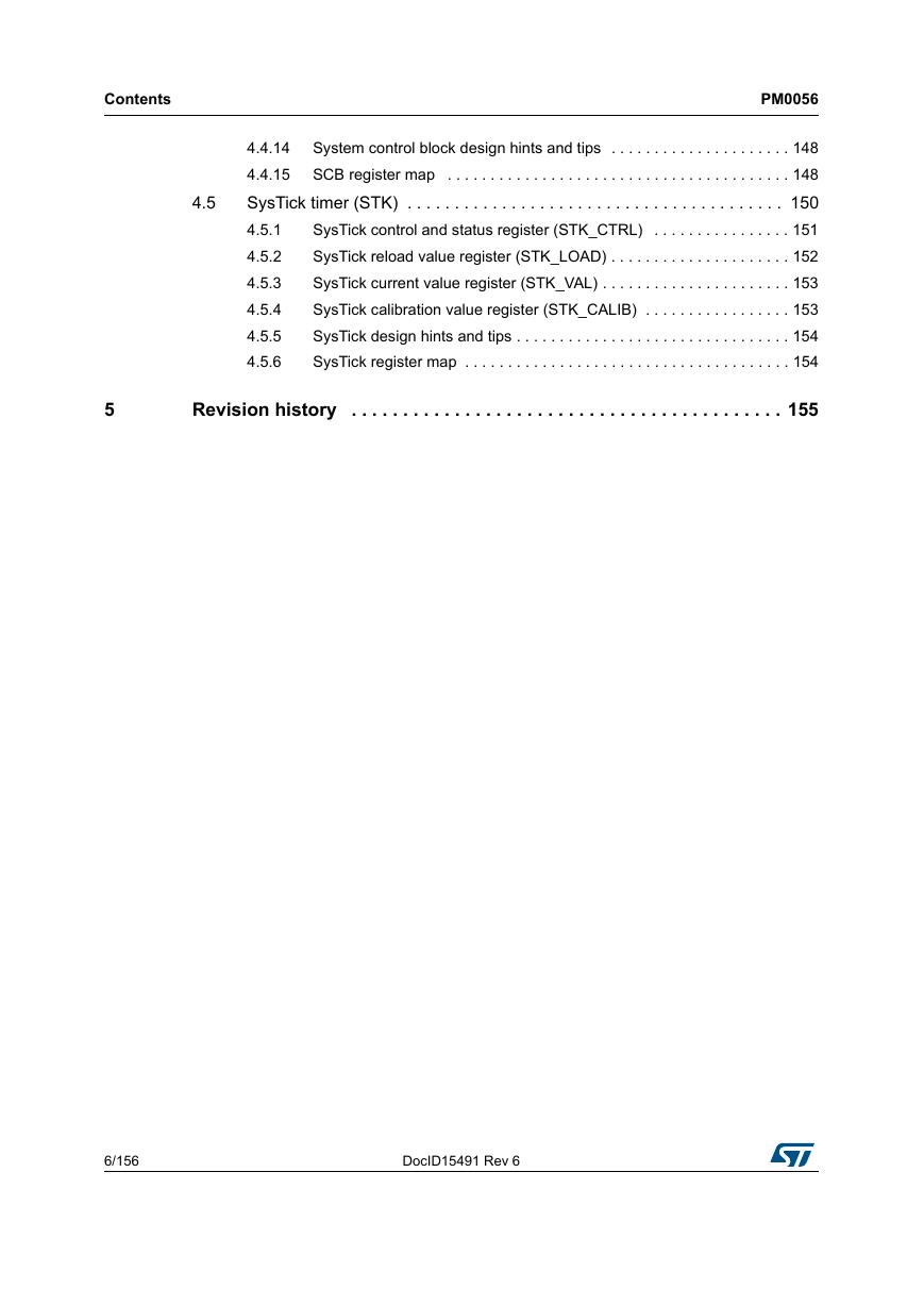
Contents PM0056 3.6 3.7 3.8 3.9 ASR, LSL, LSR, ROR, and RRX . . . . . . . . . . . . . . . . . . . . . . . . . . . . . . 76 3.5.3 CLZ . . . . . . . . . . . . . . . . . . . . . . . . . . . . . . . . . . . . . . . . . . . . . . . . . . . . 77 3.5.4 CMP and CMN . . . . . . . . . . . . . . . . . . . . . . . . . . . . . . . . . . . . . . . . . . . . 78 3.5.5 MOV and MVN . . . . . . . . . . . . . . . . . . . . . . . . . . . . . . . . . . . . . . . . . . . . 79 3.5.6 MOVT . . . . . . . . . . . . . . . . . . . . . . . . . . . . . . . . . . . . . . . . . . . . . . . . . . 80 3.5.7 REV, REV16, REVSH, and RBIT . . . . . . . . . . . . . . . . . . . . . . . . . . . . . . 81 3.5.8 3.5.9 TST and TEQ . . . . . . . . . . . . . . . . . . . . . . . . . . . . . . . . . . . . . . . . . . . . . 82 Multiply and divide instructions . . . . . . . . . . . . . . . . . . . . . . . . . . . . . . . . . 83 3.6.1 MUL, MLA, and MLS . . . . . . . . . . . . . . . . . . . . . . . . . . . . . . . . . . . . . . . 83 UMULL, UMLAL, SMULL, and SMLAL . . . . . . . . . . . . . . . . . . . . . . . . . 85 3.6.2 3.6.3 SDIV and UDIV . . . . . . . . . . . . . . . . . . . . . . . . . . . . . . . . . . . . . . . . . . . 86 Saturating instructions . . . . . . . . . . . . . . . . . . . . . . . . . . . . . . . . . . . . . . . 87 3.7.1 SSAT and USAT . . . . . . . . . . . . . . . . . . . . . . . . . . . . . . . . . . . . . . . . . . 87 Bitfield instructions . . . . . . . . . . . . . . . . . . . . . . . . . . . . . . . . . . . . . . . . . . 88 BFC and BFI . . . . . . . . . . . . . . . . . . . . . . . . . . . . . . . . . . . . . . . . . . . . . 89 3.8.1 SBFX and UBFX . . . . . . . . . . . . . . . . . . . . . . . . . . . . . . . . . . . . . . . . . . 89 3.8.2 3.8.3 SXT and UXT . . . . . . . . . . . . . . . . . . . . . . . . . . . . . . . . . . . . . . . . . . . . . 90 Branch and control instructions . . . . . . . . . . . . . . . . . . . . . . . . . . . . . . . 91 3.8.4 B, BL, BX, and BLX . . . . . . . . . . . . . . . . . . . . . . . . . . . . . . . . . . . . . . . . 92 3.8.5 3.8.6 CBZ and CBNZ . . . . . . . . . . . . . . . . . . . . . . . . . . . . . . . . . . . . . . . . . . . 93 IT . . . . . . . . . . . . . . . . . . . . . . . . . . . . . . . . . . . . . . . . . . . . . . . . . . . . . . 94 3.8.7 3.8.8 TBB and TBH . . . . . . . . . . . . . . . . . . . . . . . . . . . . . . . . . . . . . . . . . . . . . 96 Miscellaneous instructions . . . . . . . . . . . . . . . . . . . . . . . . . . . . . . . . . . . . 97 BKPT . . . . . . . . . . . . . . . . . . . . . . . . . . . . . . . . . . . . . . . . . . . . . . . . . . . 98 3.9.1 CPS . . . . . . . . . . . . . . . . . . . . . . . . . . . . . . . . . . . . . . . . . . . . . . . . . . . . 98 3.9.2 3.9.3 DMB . . . . . . . . . . . . . . . . . . . . . . . . . . . . . . . . . . . . . . . . . . . . . . . . . . . . 99 DSB . . . . . . . . . . . . . . . . . . . . . . . . . . . . . . . . . . . . . . . . . . . . . . . . . . . 100 3.9.4 ISB . . . . . . . . . . . . . . . . . . . . . . . . . . . . . . . . . . . . . . . . . . . . . . . . . . . . 100 3.9.5 3.9.6 MRS . . . . . . . . . . . . . . . . . . . . . . . . . . . . . . . . . . . . . . . . . . . . . . . . . . . 100 MSR . . . . . . . . . . . . . . . . . . . . . . . . . . . . . . . . . . . . . . . . . . . . . . . . . . . 101 3.9.7 NOP . . . . . . . . . . . . . . . . . . . . . . . . . . . . . . . . . . . . . . . . . . . . . . . . . . . 102 3.9.8 3.9.9 SEV . . . . . . . . . . . . . . . . . . . . . . . . . . . . . . . . . . . . . . . . . . . . . . . . . . . 102 3.9.10 SVC . . . . . . . . . . . . . . . . . . . . . . . . . . . . . . . . . . . . . . . . . . . . . . . . . . . 103 3.9.11 WFE . . . . . . . . . . . . . . . . . . . . . . . . . . . . . . . . . . . . . . . . . . . . . . . . . . . 103 3.9.12 WFI . . . . . . . . . . . . . . . . . . . . . . . . . . . . . . . . . . . . . . . . . . . . . . . . . . . 104 4 4/156 Core peripherals . . . . . . . . . . . . . . . . . . . . . . . . . . . . . . . . . . . . . . . . . . 105 DocID15491 Rev 6
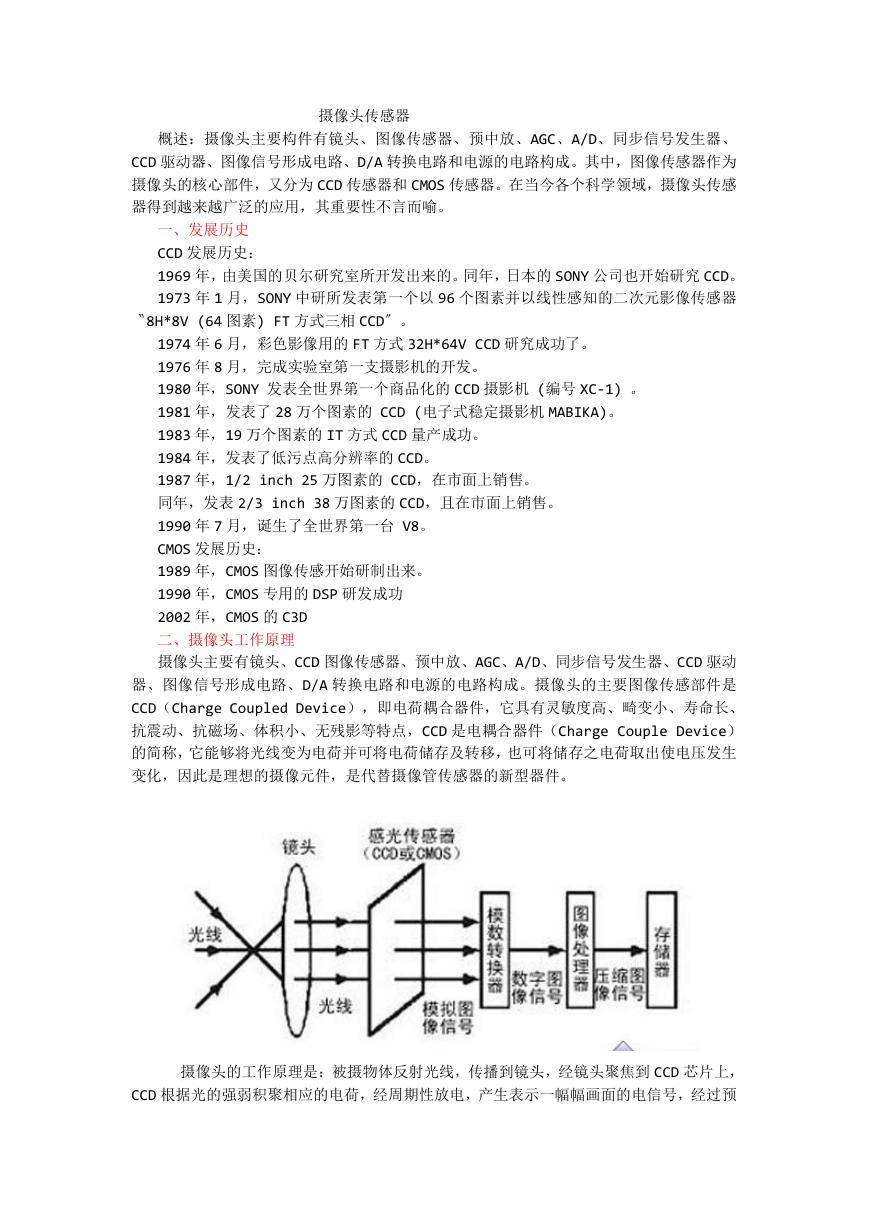
PM0056 Contents 4.1 4.2 4.3 4.4 About the STM32 core peripherals . . . . . . . . . . . . . . . . . . . . . . . . . . . . . 105 Memory protection unit (MPU) . . . . . . . . . . . . . . . . . . . . . . . . . . . . . . . . 105 4.2.1 MPU access permission attributes . . . . . . . . . . . . . . . . . . . . . . . . . . . 106 MPU mismatch . . . . . . . . . . . . . . . . . . . . . . . . . . . . . . . . . . . . . . . . . . 108 4.2.2 Updating an MPU region . . . . . . . . . . . . . . . . . . . . . . . . . . . . . . . . . . . 108 4.2.3 4.2.4 MPU design hints and tips . . . . . . . . . . . . . . . . . . . . . . . . . . . . . . . . . . 110 MPU type register (MPU_TYPER) . . . . . . . . . . . . . . . . . . . . . . . . . . . . 111 4.2.5 MPU control register (MPU_CR) . . . . . . . . . . . . . . . . . . . . . . . . . . . . . 112 4.2.6 4.2.7 MPU region number register (MPU_RNR) . . . . . . . . . . . . . . . . . . . . . 113 MPU region base address register (MPU_RBAR) . . . . . . . . . . . . . . . . 114 4.2.8 4.2.9 MPU region attribute and size register (MPU_RASR) . . . . . . . . . . . . . 116 Nested vectored interrupt controller (NVIC) . . . . . . . . . . . . . . . . . . . . . . .118 The CMSIS mapping of the Cortex®-M3 NVIC registers . . . . . . . . . . . 119 4.3.1 4.3.2 Interrupt set-enable registers (NVIC_ISERx) . . . . . . . . . . . . . . . . . . . . 120 Interrupt clear-enable registers (NVIC_ICERx) . . . . . . . . . . . . . . . . . . 121 4.3.3 Interrupt set-pending registers (NVIC_ISPRx) . . . . . . . . . . . . . . . . . . . 122 4.3.4 4.3.5 Interrupt clear-pending registers (NVIC_ICPRx) . . . . . . . . . . . . . . . . . 123 Interrupt active bit registers (NVIC_IABRx) . . . . . . . . . . . . . . . . . . . . . 124 4.3.6 Interrupt priority registers (NVIC_IPRx) . . . . . . . . . . . . . . . . . . . . . . . . 125 4.3.7 4.3.8 Software trigger interrupt register (NVIC_STIR) . . . . . . . . . . . . . . . . . 126 Level-sensitive and pulse interrupts . . . . . . . . . . . . . . . . . . . . . . . . . . 126 4.3.9 NVIC design hints and tips . . . . . . . . . . . . . . . . . . . . . . . . . . . . . . . . . 127 4.3.10 4.3.11 NVIC register map . . . . . . . . . . . . . . . . . . . . . . . . . . . . . . . . . . . . . . . . 128 System control block (SCB) . . . . . . . . . . . . . . . . . . . . . . . . . . . . . . . . . . 129 Auxiliary control register (SCB_ACTLR) . . . . . . . . . . . . . . . . . . . . . . . 129 4.4.1 4.4.2 CPUID base register (SCB_CPUID) . . . . . . . . . . . . . . . . . . . . . . . . . . 130 Interrupt control and state register (SCB_ICSR) . . . . . . . . . . . . . . . . . 131 4.4.3 Vector table offset register (SCB_VTOR) . . . . . . . . . . . . . . . . . . . . . . 133 4.4.4 4.4.5 Application interrupt and reset control register (SCB_AIRCR) . . . . . . 134 System control register (SCB_SCR) . . . . . . . . . . . . . . . . . . . . . . . . . . 136 4.4.6 Configuration and control register (SCB_CCR) . . . . . . . . . . . . . . . . . . 137 4.4.7 4.4.8 System handler priority registers (SHPRx) . . . . . . . . . . . . . . . . . . . . . 138 System handler control and state register (SCB_SHCSR) . . . . . . . . . 140 4.4.9 4.4.10 Configurable fault status register (SCB_CFSR) . . . . . . . . . . . . . . . . . 142 4.4.11 Hard fault status register (SCB_HFSR) . . . . . . . . . . . . . . . . . . . . . . . . 145 4.4.12 Memory management fault address register (SCB_MMFAR) . . . . . . . 147 4.4.13 Bus fault address register (SCB_BFAR) . . . . . . . . . . . . . . . . . . . . . . . 147 DocID15491 Rev 6 5/156 6
Contents 4.5 PM0056 System control block design hints and tips . . . . . . . . . . . . . . . . . . . . . 148 4.4.14 4.4.15 SCB register map . . . . . . . . . . . . . . . . . . . . . . . . . . . . . . . . . . . . . . . . 148 SysTick timer (STK) . . . . . . . . . . . . . . . . . . . . . . . . . . . . . . . . . . . . . . . . 150 SysTick control and status register (STK_CTRL) . . . . . . . . . . . . . . . . 151 4.5.1 SysTick reload value register (STK_LOAD) . . . . . . . . . . . . . . . . . . . . . 152 4.5.2 4.5.3 SysTick current value register (STK_VAL) . . . . . . . . . . . . . . . . . . . . . . 153 SysTick calibration value register (STK_CALIB) . . . . . . . . . . . . . . . . . 153 4.5.4 SysTick design hints and tips . . . . . . . . . . . . . . . . . . . . . . . . . . . . . . . . 154 4.5.5 4.5.6 SysTick register map . . . . . . . . . . . . . . . . . . . . . . . . . . . . . . . . . . . . . . 154 5 Revision history . . . . . . . . . . . . . . . . . . . . . . . . . . . . . . . . . . . . . . . . . . 155 6/156 DocID15491 Rev 6
PM0056 List of tables List of tables Summary of processor mode, execution privilege level, and stack use options. . . . . . . . . 14 Table 1. Core register set summary . . . . . . . . . . . . . . . . . . . . . . . . . . . . . . . . . . . . . . . . . . . . . . . . . 15 Table 2. PSR register combinations . . . . . . . . . . . . . . . . . . . . . . . . . . . . . . . . . . . . . . . . . . . . . . . . . 16 Table 3. APSR bit definitions . . . . . . . . . . . . . . . . . . . . . . . . . . . . . . . . . . . . . . . . . . . . . . . . . . . . . . 17 Table 4. IPSR bit definitions . . . . . . . . . . . . . . . . . . . . . . . . . . . . . . . . . . . . . . . . . . . . . . . . . . . . . . . 18 Table 5. EPSR bit definitions . . . . . . . . . . . . . . . . . . . . . . . . . . . . . . . . . . . . . . . . . . . . . . . . . . . . . . 19 Table 6. PRIMASK register bit definitions. . . . . . . . . . . . . . . . . . . . . . . . . . . . . . . . . . . . . . . . . . . . . 20 Table 7. FAULTMASK register bit definitions . . . . . . . . . . . . . . . . . . . . . . . . . . . . . . . . . . . . . . . . . . 20 Table 8. BASEPRI register bit assignments . . . . . . . . . . . . . . . . . . . . . . . . . . . . . . . . . . . . . . . . . . . 21 Table 9. Table 10. CONTROL register bit definitions . . . . . . . . . . . . . . . . . . . . . . . . . . . . . . . . . . . . . . . . . . . . 22 Table 11. Ordering of memory accesses . . . . . . . . . . . . . . . . . . . . . . . . . . . . . . . . . . . . . . . . . . . . . . 25 Table 12. Memory access behavior . . . . . . . . . . . . . . . . . . . . . . . . . . . . . . . . . . . . . . . . . . . . . . . . . . 26 Table 13. SRAM memory bit-banding regions . . . . . . . . . . . . . . . . . . . . . . . . . . . . . . . . . . . . . . . . . . 28 Peripheral memory bit-banding regions . . . . . . . . . . . . . . . . . . . . . . . . . . . . . . . . . . . . . . . 28 Table 14. C compiler intrinsic functions for exclusive access instructions . . . . . . . . . . . . . . . . . . . . . 31 Table 15. Properties of the different exception types . . . . . . . . . . . . . . . . . . . . . . . . . . . . . . . . . . . . . 33 Table 16. Table 17. Exception return behavior. . . . . . . . . . . . . . . . . . . . . . . . . . . . . . . . . . . . . . . . . . . . . . . . . . 39 Faults . . . . . . . . . . . . . . . . . . . . . . . . . . . . . . . . . . . . . . . . . . . . . . . . . . . . . . . . . . . . . . . . . 40 Table 18. Fault status and fault address registers . . . . . . . . . . . . . . . . . . . . . . . . . . . . . . . . . . . . . . . 41 Table 19. Cortex-M3 instructions . . . . . . . . . . . . . . . . . . . . . . . . . . . . . . . . . . . . . . . . . . . . . . . . . . . . 44 Table 20. Table 21. CMSIS intrinsic functions to generate some Cortex-M3 instructions . . . . . . . . . . . . . . . . . 49 CMSIS intrinsic functions to access the special registers. . . . . . . . . . . . . . . . . . . . . . . . . . 50 Table 22. Table 23. Condition code suffixes. . . . . . . . . . . . . . . . . . . . . . . . . . . . . . . . . . . . . . . . . . . . . . . . . . . . 57 Table 24. Memory access instructions . . . . . . . . . . . . . . . . . . . . . . . . . . . . . . . . . . . . . . . . . . . . . . . . 59 Table 25. Immediate, pre-indexed and post-indexed offset ranges . . . . . . . . . . . . . . . . . . . . . . . . . . 62 label-PC offset ranges . . . . . . . . . . . . . . . . . . . . . . . . . . . . . . . . . . . . . . . . . . . . . . . . . . . . 66 Table 26. Table 27. Data processing instructions. . . . . . . . . . . . . . . . . . . . . . . . . . . . . . . . . . . . . . . . . . . . . . . . 72 Table 28. Multiply and divide instructions . . . . . . . . . . . . . . . . . . . . . . . . . . . . . . . . . . . . . . . . . . . . . . 83 Table 29. Packing and unpacking instructions . . . . . . . . . . . . . . . . . . . . . . . . . . . . . . . . . . . . . . . . . . 88 Branch and control instructions . . . . . . . . . . . . . . . . . . . . . . . . . . . . . . . . . . . . . . . . . . . . . 91 Table 30. Table 31. Branch ranges . . . . . . . . . . . . . . . . . . . . . . . . . . . . . . . . . . . . . . . . . . . . . . . . . . . . . . . . . . 92 Table 32. Miscellaneous instructions . . . . . . . . . . . . . . . . . . . . . . . . . . . . . . . . . . . . . . . . . . . . . . . . . 97 Table 33. STM32 core peripheral register regions . . . . . . . . . . . . . . . . . . . . . . . . . . . . . . . . . . . . . . 105 Table 34. Memory attributes summary . . . . . . . . . . . . . . . . . . . . . . . . . . . . . . . . . . . . . . . . . . . . . . . 106 TEX, C, B, and S encoding. . . . . . . . . . . . . . . . . . . . . . . . . . . . . . . . . . . . . . . . . . . . . . . . 107 Table 35. Cache policy for memory attribute encoding . . . . . . . . . . . . . . . . . . . . . . . . . . . . . . . . . . 107 Table 36. Table 37. AP encoding . . . . . . . . . . . . . . . . . . . . . . . . . . . . . . . . . . . . . . . . . . . . . . . . . . . . . . . . . . . 108 Table 38. Memory region attributes for STM32 . . . . . . . . . . . . . . . . . . . . . . . . . . . . . . . . . . . . . . . . 111 Table 39. Example SIZE field values . . . . . . . . . . . . . . . . . . . . . . . . . . . . . . . . . . . . . . . . . . . . . . . . 117 Table 40. MPU register map and reset values . . . . . . . . . . . . . . . . . . . . . . . . . . . . . . . . . . . . . . . . . 117 Table 41. Mapping of interrupts to the interrupt variables . . . . . . . . . . . . . . . . . . . . . . . . . . . . . . . . 119 Table 42. IPR bit assignments . . . . . . . . . . . . . . . . . . . . . . . . . . . . . . . . . . . . . . . . . . . . . . . . . . . . . 125 CMSIS functions for NVIC control . . . . . . . . . . . . . . . . . . . . . . . . . . . . . . . . . . . . . . . . . . 127 Table 43. NVIC register map and reset values. . . . . . . . . . . . . . . . . . . . . . . . . . . . . . . . . . . . . . . . . 128 Table 44. Priority grouping . . . . . . . . . . . . . . . . . . . . . . . . . . . . . . . . . . . . . . . . . . . . . . . . . . . . . . . . 135 Table 45. Table 46. System fault handler priority fields . . . . . . . . . . . . . . . . . . . . . . . . . . . . . . . . . . . . . . . . . . 138 SCB register map and reset value for STM32F2 and STM32L . . . . . . . . . . . . . . . . . . . . 148 Table 47. Table 48. SCB register map and reset values . . . . . . . . . . . . . . . . . . . . . . . . . . . . . . . . . . . . . . . . . 149 DocID15491 Rev 6 7/156 8
List of tables PM0056 Table 49. Table 50. SysTick register map and reset values. . . . . . . . . . . . . . . . . . . . . . . . . . . . . . . . . . . . . . . 154 Document revision history . . . . . . . . . . . . . . . . . . . . . . . . . . . . . . . . . . . . . . . . . . . . . . . . 155 8/156 DocID15491 Rev 6
分享到:
收藏