REV
A
B
C
D
CHANGE DESCRIPTION
Release
Changed VDDCR Bypass Capacitor Value
Added CLKIN Voltage Levels At Reduced VDDIO Voltage Levels
Added Required REFCLKO Timing Analysis
NAME
DATE
06-04-10
01-19-11
01-27-12
07-25-12
Any assistance, services, comments, information, or suggestions provided by SMSC (including without limitation any comments to the
effect that the Company’s product designs do not require any changes) (collectively, “SMSC Feedback”) are provided solely for the purpose
of assisting the Company in the Company’s attempt to optimize compatibility of the Company’s product designs with certain SMSC
products. SMSC does not promise that such compatibility optimization will actually be achieved. Circuit diagrams utilizing SMSC products
are included as a means of illustrating typical applications; consequently, complete information sufficient for construction purposes is not
necessarily given. Although the information has been checked and is believed to be accurate, no responsibility is assumed for inaccuracies.
SMSC reserves the right to make changes to specifications and product descriptions at any time without notice.
DOCUMENT DESCRIPTION
Schematic Checklist for the LAN8720, 24-pin QFN Package
SMSC
80 Arkay Drive
Hauppauge, New York 11788
Document Number
SC471228
Revision
D
�
Schematic Checklist for LAN8720
Information Particular to the 24-pin QFN Package
LAN8720 QFN PHY Interface:
1. TXP (pin 21): This pin is the transmit twisted pair output positive connection from the
internal PHY. It requires a 49.9, 1.0% pull-up resistor to VDDA (created from +3.3V).
This pin also connects to the transmit channel of the magnetics.
2. TXN (pin 20): This pin is the transmit twisted pair output negative connection from the
internal PHY. It requires a 49.9, 1.0% pull-up resistor to VDDA (created from +3.3V).
This pin also connects to the transmit channel of the magnetics.
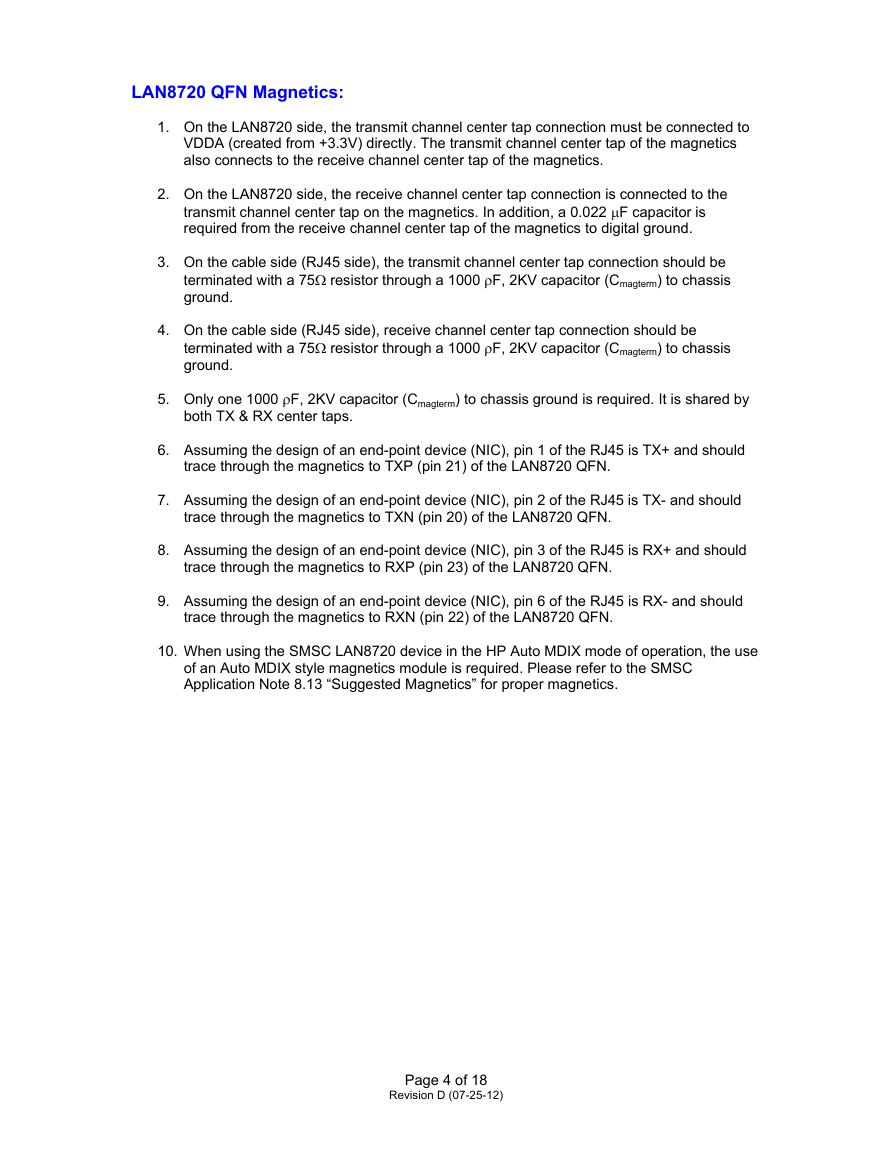
3. For transmit channel connection and termination details, refer to Figure 1.
4. RXP (pin 23): This pin is the receive twisted pair input positive connection to the internal
PHY. It requires a 49.9, 1.0% pull-up resistor to VDDA (created from +3.3V). This pin
also connects to the receive channel of the magnetics.
5. RXN (pin 22): This pin is the receive twisted pair input negative connection to the internal
PHY. It requires a 49.9, 1.0% pull-up resistor to VDDA (created from +3.3V). This pin
also connects to the receive channel of the magnetics.
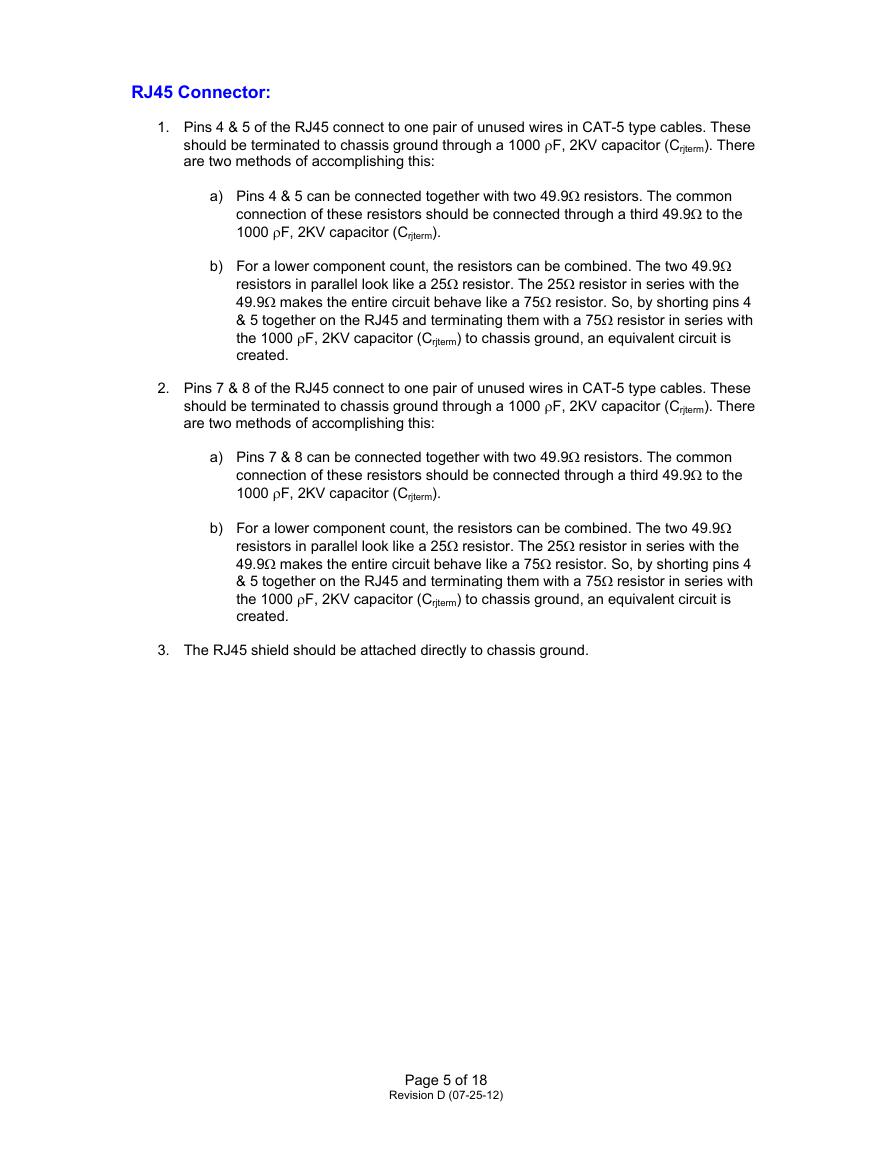
6. For receive channel connection and termination details, refer to Figure 2.
7. For added EMC flexibility in a LAN8720 design, the designer should include four low
valued capacitors on the TXP, TXN, RXP & RXN pins. Low valued capacitors (22 F or
less) can be added to each line and terminated to digital ground. These components can
be added to the schematic and should be designated as Do Not Populate (DNP).
Page 2 of 18
Revision D (07-25-12)
�
VDDA (+3.3V)
A
1
D
D
V
A
2
D
D
V
R3
49.9 Ohms
1.0%
R4
49.9 Ohms
1.0%
LAN8720
21
20
TXP
TXN
Magnetics Module
Transmit Channel
TD+
TCT
TD-
Connect TX
Center Tap to RX
Center Tap
Figure 1 – Transmit Channel Connections and Terminations
VDDA (+3.3V)
A
1
D
D
V
A
2
D
D
V
R1
49.9 Ohms
1.0%
R2
49.9 Ohms
1.0%
LAN8720
23
22
RXP
RXN
Connect RX
Center Tap to TX
Center Tap
Magnetics Module
Receive Channel
RD+
RCT
RD-
C1
0.022 uF
Figure 2 – Receive Channel Connections and Terminations
Page 3 of 18
Revision D (07-25-12)
TX
+
TCMT
TX-
RX+
RCMT
RX-
�
LAN8720 QFN Magnetics:
1. On the LAN8720 side, the transmit channel center tap connection must be connected to
VDDA (created from +3.3V) directly. The transmit channel center tap of the magnetics
also connects to the receive channel center tap of the magnetics.
2. On the LAN8720 side, the receive channel center tap connection is connected to the
transmit channel center tap on the magnetics. In addition, a 0.022 F capacitor is
required from the receive channel center tap of the magnetics to digital ground.
3. On the cable side (RJ45 side), the transmit channel center tap connection should be
terminated with a 75 resistor through a 1000 F, 2KV capacitor (Cmagterm) to chassis
ground.
4. On the cable side (RJ45 side), receive channel center tap connection should be
terminated with a 75 resistor through a 1000 F, 2KV capacitor (Cmagterm) to chassis
ground.
5. Only one 1000 F, 2KV capacitor (Cmagterm) to chassis ground is required. It is shared by
both TX & RX center taps.
6. Assuming the design of an end-point device (NIC), pin 1 of the RJ45 is TX+ and should
trace through the magnetics to TXP (pin 21) of the LAN8720 QFN.
7. Assuming the design of an end-point device (NIC), pin 2 of the RJ45 is TX- and should
trace through the magnetics to TXN (pin 20) of the LAN8720 QFN.
8. Assuming the design of an end-point device (NIC), pin 3 of the RJ45 is RX+ and should
trace through the magnetics to RXP (pin 23) of the LAN8720 QFN.
9. Assuming the design of an end-point device (NIC), pin 6 of the RJ45 is RX- and should
trace through the magnetics to RXN (pin 22) of the LAN8720 QFN.
10. When using the SMSC LAN8720 device in the HP Auto MDIX mode of operation, the use
of an Auto MDIX style magnetics module is required. Please refer to the SMSC
Application Note 8.13 “Suggested Magnetics” for proper magnetics.
Page 4 of 18
Revision D (07-25-12)
�
RJ45 Connector:
1. Pins 4 & 5 of the RJ45 connect to one pair of unused wires in CAT-5 type cables. These
should be terminated to chassis ground through a 1000 F, 2KV capacitor (Crjterm). There
are two methods of accomplishing this:
a) Pins 4 & 5 can be connected together with two 49.9 resistors. The common
connection of these resistors should be connected through a third 49.9 to the
1000 F, 2KV capacitor (Crjterm).
b) For a lower component count, the resistors can be combined. The two 49.9
resistors in parallel look like a 25 resistor. The 25 resistor in series with the
49.9 makes the entire circuit behave like a 75 resistor. So, by shorting pins 4
& 5 together on the RJ45 and terminating them with a 75 resistor in series with
the 1000 F, 2KV capacitor (Crjterm) to chassis ground, an equivalent circuit is
created.
2. Pins 7 & 8 of the RJ45 connect to one pair of unused wires in CAT-5 type cables. These
should be terminated to chassis ground through a 1000 F, 2KV capacitor (Crjterm). There
are two methods of accomplishing this:
a) Pins 7 & 8 can be connected together with two 49.9 resistors. The common
connection of these resistors should be connected through a third 49.9 to the
1000 F, 2KV capacitor (Crjterm).
b) For a lower component count, the resistors can be combined. The two 49.9
resistors in parallel look like a 25 resistor. The 25 resistor in series with the
49.9 makes the entire circuit behave like a 75 resistor. So, by shorting pins 4
& 5 together on the RJ45 and terminating them with a 75 resistor in series with
the 1000 F, 2KV capacitor (Crjterm) to chassis ground, an equivalent circuit is
created.
3. The RJ45 shield should be attached directly to chassis ground.
Page 5 of 18
Revision D (07-25-12)
�
Power Supply Connections:
1. The analog supply (VDD1A & VDD2A) pins on the LAN8720 QFN are 1 & 19. They
require a connection to VDDA (created from +3.3V through a ferrite bead). Be sure to
place bulk capacitance on each side of the ferrite bead.
Note: Pins 1 & 19 (VDD1A & VDD2A) must always be connected to a +3.3V power
supply; even in the case of having the internal +1.2V regulator of the LAN8720 disabled.
Other blocks within the LAN8720 require power from +3.3V.
2. Each VDDxA pin should have one .01 F (or smaller) capacitor to decouple the
LAN8720. The capacitor size should be SMD_0603 or smaller.
3. Pin 9 (VDDIO) is a variable supply voltage for the I/O pads. This pin must be connected
to a voltage supply between +1.8V and +3.3V. The VDDIO power plane should have
proper bulk capacitance.
4. The VDDIO pin should have one .01 F (or smaller) capacitor to decouple the LAN8720.
The capacitor size should be SMD_0603 or smaller.
Ground Connections:
1. The digital ground pins (GND), the analog ground pins (AVSS), and the GND_CORE pins
on the LAN8720 QFN are all connected internally to the exposed die paddle ground. The
EDP Ground pad on the underside of the LAN8720 must be connected directly to a solid,
contiguous digital ground plane.
2.
It is recommended that all ground connections be tied together to the same ground plane.
It is not recommended to run separate ground planes for any SMSC LAN products.
Page 6 of 18
Revision D (07-25-12)
�
VDDCR:
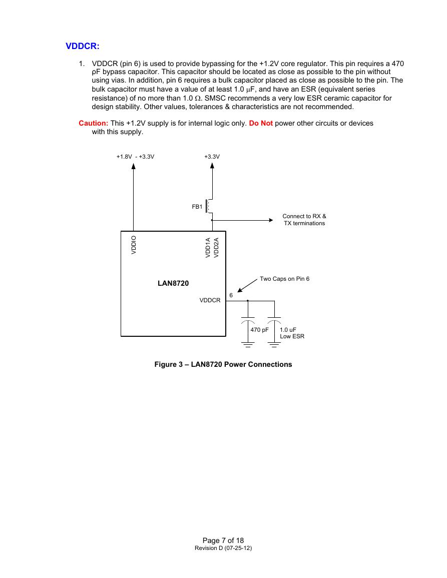
1. VDDCR (pin 6) is used to provide bypassing for the +1.2V core regulator. This pin requires a 470
ρF bypass capacitor. This capacitor should be located as close as possible to the pin without
using vias. In addition, pin 6 requires a bulk capacitor placed as close as possible to the pin. The
bulk capacitor must have a value of at least 1.0 F, and have an ESR (equivalent series
resistance) of no more than 1.0 . SMSC recommends a very low ESR ceramic capacitor for
design stability. Other values, tolerances & characteristics are not recommended.
Caution: This +1.2V supply is for internal logic only. Do Not power other circuits or devices
with this supply.
+1.8V - +3.3V
+3.3V
FB1
A
1
D
D
V
A
2
D
D
V
I
O
D
D
V
Connect to RX &
TX terminations
LAN8720
6
VDDCR
Two Caps on Pin 6
470 pF
1.0 uF
Low ESR
Figure 3 – LAN8720 Power Connections
Page 7 of 18
Revision D (07-25-12)
�
Crystal Connections:
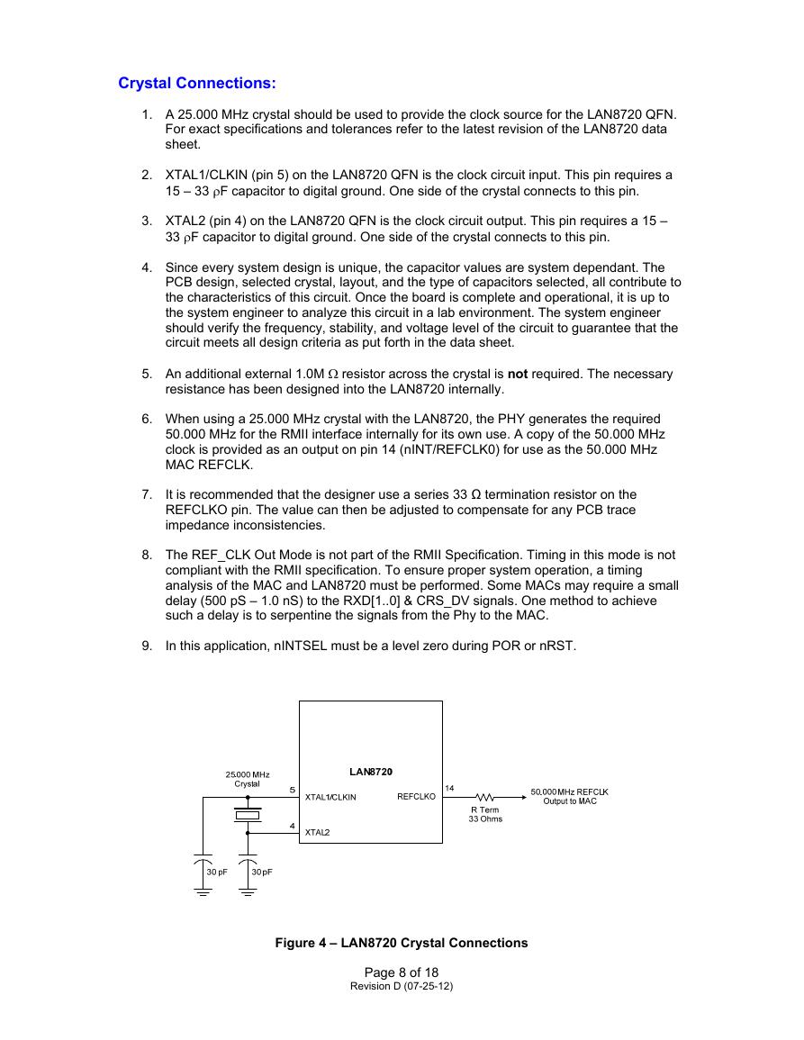
1. A 25.000 MHz crystal should be used to provide the clock source for the LAN8720 QFN.
For exact specifications and tolerances refer to the latest revision of the LAN8720 data
sheet.
2. XTAL1/CLKIN (pin 5) on the LAN8720 QFN is the clock circuit input. This pin requires a
15 – 33 F capacitor to digital ground. One side of the crystal connects to this pin.
3. XTAL2 (pin 4) on the LAN8720 QFN is the clock circuit output. This pin requires a 15 –
33 F capacitor to digital ground. One side of the crystal connects to this pin.
4. Since every system design is unique, the capacitor values are system dependant. The
PCB design, selected crystal, layout, and the type of capacitors selected, all contribute to
the characteristics of this circuit. Once the board is complete and operational, it is up to
the system engineer to analyze this circuit in a lab environment. The system engineer
should verify the frequency, stability, and voltage level of the circuit to guarantee that the
circuit meets all design criteria as put forth in the data sheet.
5. An additional external 1.0M resistor across the crystal is not required. The necessary
resistance has been designed into the LAN8720 internally.
6. When using a 25.000 MHz crystal with the LAN8720, the PHY generates the required
50.000 MHz for the RMII interface internally for its own use. A copy of the 50.000 MHz
clock is provided as an output on pin 14 (nINT/REFCLK0) for use as the 50.000 MHz
MAC REFCLK.
7.
It is recommended that the designer use a series 33 Ω termination resistor on the
REFCLKO pin. The value can then be adjusted to compensate for any PCB trace
impedance inconsistencies.
8. The REF_CLK Out Mode is not part of the RMII Specification. Timing in this mode is not
compliant with the RMII specification. To ensure proper system operation, a timing
analysis of the MAC and LAN8720 must be performed. Some MACs may require a small
delay (500 pS – 1.0 nS) to the RXD[1..0] & CRS_DV signals. One method to achieve
such a delay is to serpentine the signals from the Phy to the MAC.
9.
In this application, nINTSEL must be a level zero during POR or nRST.
Figure 4 – LAN8720 Crystal Connections
Page 8 of 18
Revision D (07-25-12)
�



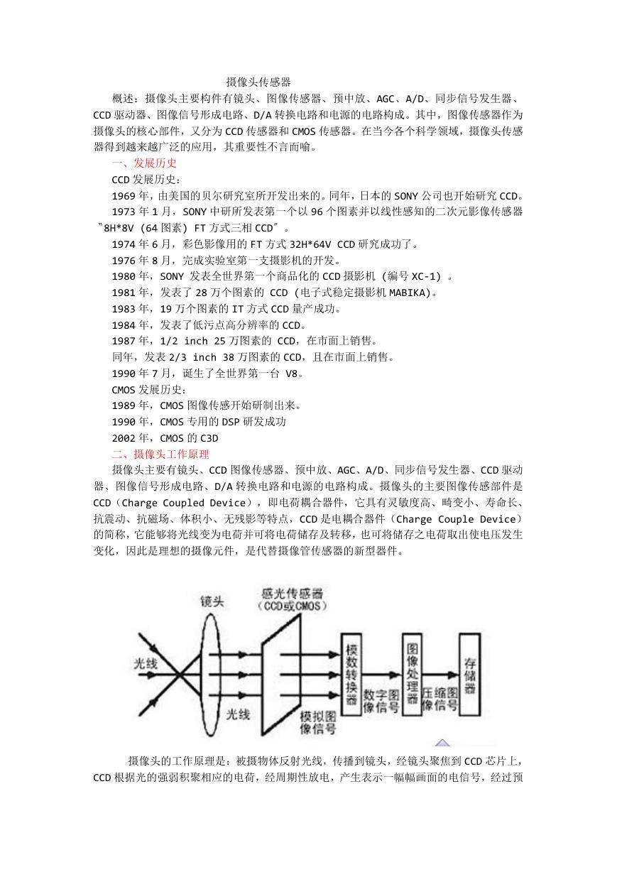
 V2版本原理图(Capacitive-Fingerprint-Reader-Schematic_V2).pdf
 摄像头工作原理.doc
 VL53L0X简要说明(En.FLVL53L00216).pdf
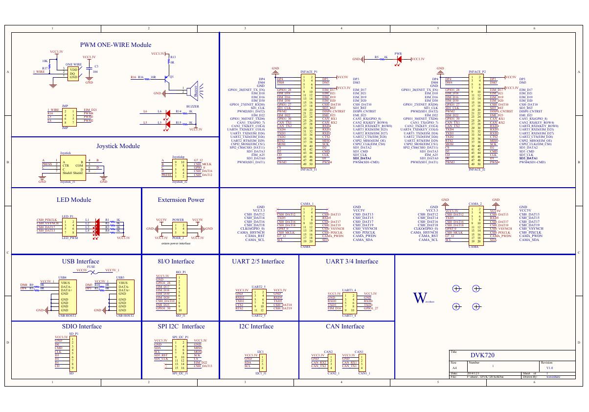 原理图(DVK720-Schematic).pdf
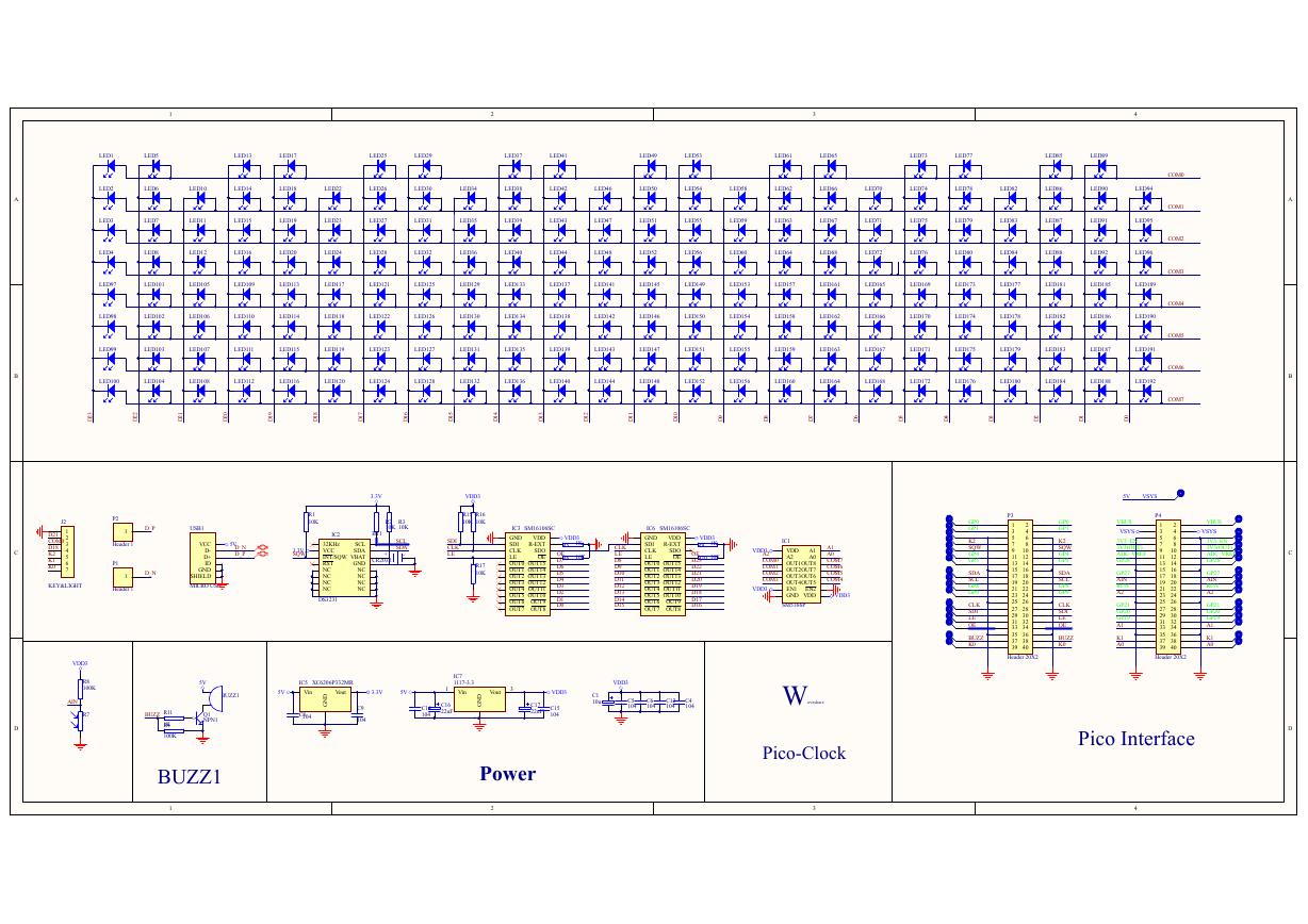 原理图(Pico-Clock-Green-Schdoc).pdf
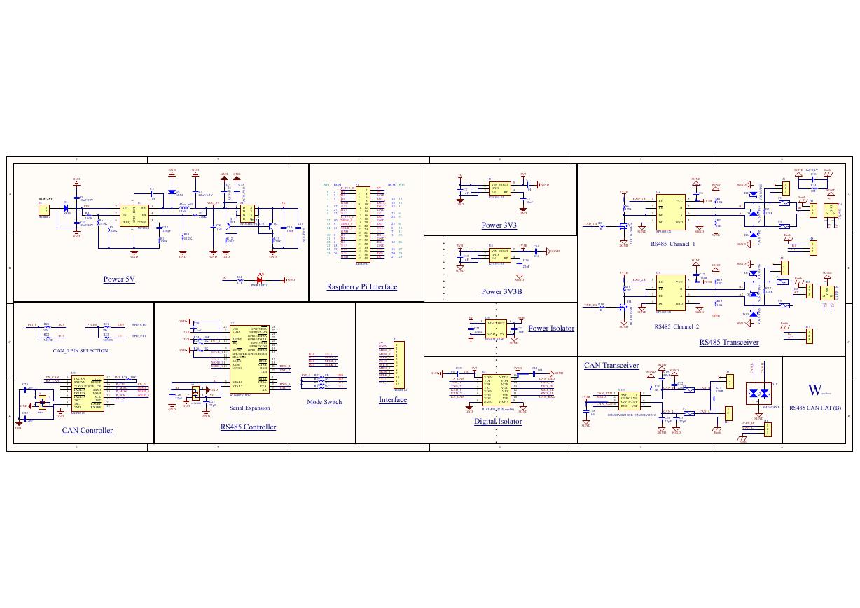 原理图(RS485-CAN-HAT-B-schematic).pdf
 File:SIM7500_SIM7600_SIM7800 Series_SSL_Application Note_V2.00.pdf
 ADS1263(Ads1262).pdf
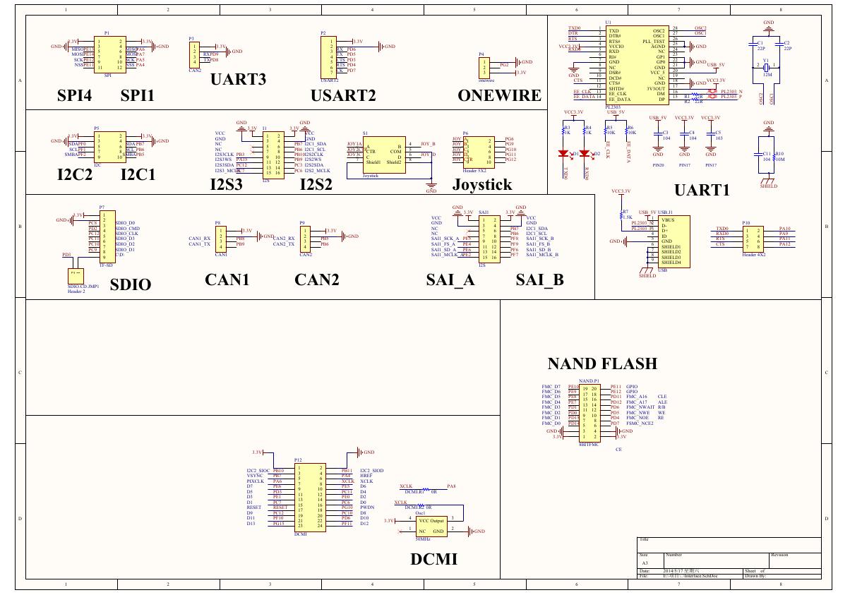 原理图(Open429Z-D-Schematic).pdf
 用户手册(Capacitive_Fingerprint_Reader_User_Manual_CN).pdf
 CY7C68013A(英文版)(CY7C68013A).pdf
 TechnicalReference_Dem.pdf