logo资料库

MCP2518FD数据手册(MCP2518FDT).pdf

第1页 / 共97页
第2页 / 共97页
第3页 / 共97页
第4页 / 共97页
第5页 / 共97页
第6页 / 共97页
第7页 / 共97页
第8页 / 共97页
资料共97页,剩余部分请下载后查看
Features
General
Message FIFOs
Message Transmission
Message Reception
Special Features
Oscillator Options
SPI Interface
Safety Critical Systems
Additional Features
Package Types
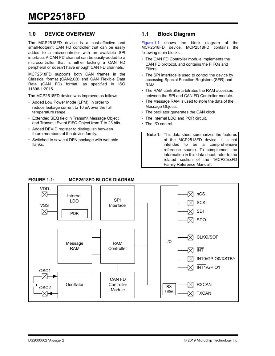
1.0 Device Overview
1.1 Block Diagram
FIGURE 1-1: MCP2518FD Block Diagram
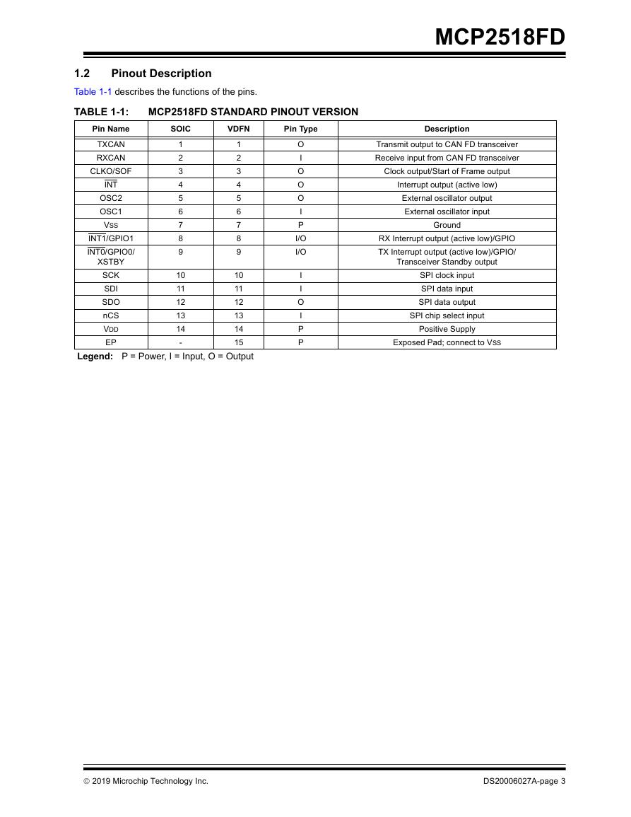
1.2 Pinout Description
TABLE 1-1: MCP2518FD STANDARD PINOUT VERSION
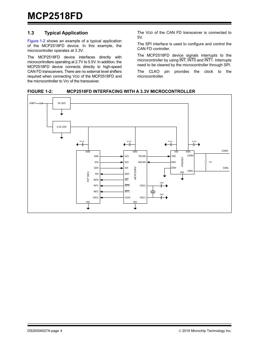
1.3 Typical Application
FIGURE 1-2: MCP2518FD interfacing with a 3.3V microcontroller
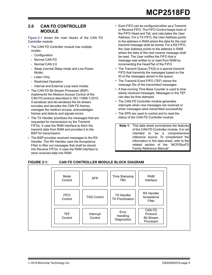
2.0 CAN FD Controller module
FIGURE 2-1: CAN FD Controller module Block Diagram
External CAN FD Controller with SPI Interface
3.0 Memory Organization
FIGURE 3-1: Memory Map
TABLE 3-1: MCP2518FD Register Summary
TABLE 3-2: CAN FD Controller module Register Summary
3.1 MCP2518FD Specific Registers
TABLE 3-3: Register Legend
EXAMPLE 3-1:
Register 3-1: OSC – MCP2518FD Oscillator Control Register
Register 3-2: IOCON – INPUT/OUTPUT Control Register
Register 3-3: CRC – CRC Register
Register 3-4: ECCCON – ECC Control Register
Register 3-5: ECCSTAT – ECC STATUS REGISTER
Register 3-6: DEVID – Device ID Register
3.2 CAN FD Controller Module Registers
TABLE 3-4: Register Legend
EXAMPLE 3-2:
Register 3-7: CiCON – CAN Control Register
Register 3-8: CiNBTCFG – Nominal Bit Time Configuration Register
Register 3-9: CiDBTCFG – Data Bit Time Configuration Register
Register 3-10: CiTDC – Transmitter Delay Compensation Register
Register 3-11: CiTBC – Time Base Counter Register
Register 3-12: CiTSCON – Time Stamp Control Register
Register 3-13: CiVEC – Interrupt Code Register
Register 3-14: CiINT – Interrupt Register
Register 3-15: CiRXIF – Receive Interrupt Status Register
Register 3-16: CiRXOVIF – Receive Overflow Interrupt Status Register
Register 3-17: CiTXIF – Transmit Interrupt Status Register
Register 3-18: CiTXATIF – Transmit Attempt Interrupt Status Register
Register 3-19: citxreq – Transmit Request Register
Register 3-20: CiTREC – Transmit/Receive Error Count Register
Register 3-21: CiBDIAG0 – bus Diagnostic Register 0
Register 3-22: CiBDIAG1 – Bus Diagnostics Register 1
Register 3-23: CiTEFCON – Transmit Event FIFO Control Register
Register 3-24: CiTEFSTA – Transmit Event FIFO Status Register
Register 3-25: CiTEFUA – Transmit Event FIFO User Address Register
Register 3-26: CiTXQCON – Transmit QUEUE Control Register
Register 3-27: CiTXQSTA – Transmit Queue Status Register
Register 3-28: citxqua – Transmit Queue User Address Register
Register 3-29: CiFIFOCONm – FIFO Control Register m, (m = 1 to 31)
Register 3-30: CiFIFOSTAm – FIFO Status Register m, (m = 1 to 31)
Register 3-31: CiFIFOUAm – FIFO User Address Register m, (m = 1 to 31)
Register 3-32: CiFLTCONm – Filter Control Register m, (m = 0 to 7)
Register 3-33: CiFLTOBJm – Filter Object Register m,(m = 0 to 31)
Register 3-34: CiMASKm – Mask Register m, (m = 0 to 31)
3.3 Message Memory
FIGURE 3-2: Message Memory organization
FIGURE 3-3: ECC Logic
TABLE 3-5: TRANSMIT MESSAGE OBJECT (TXQ AND TX FIFO)
TABLE 3-6: RECEIVE MESSAGE OBJECT
TABLE 3-7: Transmit Event FIFO Object
4.0 SPI Interface
FIGURE 4-1: SPI Instruction Format
TABLE 4-1: SPI Instructions
4.1 SFR Access
FIGURE 4-2: Reset Instruction
FIGURE 4-3: SFR Read Instruction
FIGURE 4-4: SFR WRITE Instruction
4.2 Message Memory Access
FIGURE 4-5: Message Memory Read Instruction
FIGURE 4-6: Message Memory WRITE Instruction
4.3 SPI Commands with CRC
FIGURE 4-7: CRC Calculation
FIGURE 4-8: SFR Read with CRC Instruction
FIGURE 4-9: SFR Write with CRC Instruction
FIGURE 4-10: SFR Write SAFE with CRC Instruction
FIGURE 4-11: message Memory Read with CRC Instruction
FIGURE 4-12: Message Memory Write with CRC Instruction
FIGURE 4-13: Message Memory Write SAFE with CRC Instruction
5.0 Oscillator
FIGURE 5-1: MCP2518FD Oscillator Block Diagram
6.0 I/O Configuration
FIGURE 6-1: Interrupt PINs
7.0 Electrical Specifications
7.1 Absolute Maximum Ratings†
TABLE 7-1: DC Characteristics
TABLE 7-2: CLKOUT and SOF AC Characteristics
TABLE 7-3: Crystal Oscillator AC Characteristics
TABLE 7-4: CAN Bit rate
TABLE 7-5: CAN RX Filter AC Characteristics
TABLE 7-6: SPI AC Characteristics
TABLE 7-7: Temperature Specifications
8.0 Typical Performance Curves
FIGURE 8-1: Average IDDS vs. Temperature.
FIGURE 8-2: Average IDDLPM vs. Temperature.
9.0 Packaging Information
9.1 Package Marking Information
Appendix A: Revision History
Revision A (April 2019)
Appendix B: CAN FD Conformance
TABLE B-1: ISO Optional Features
Product Identification System
Worldwide Sales and Service
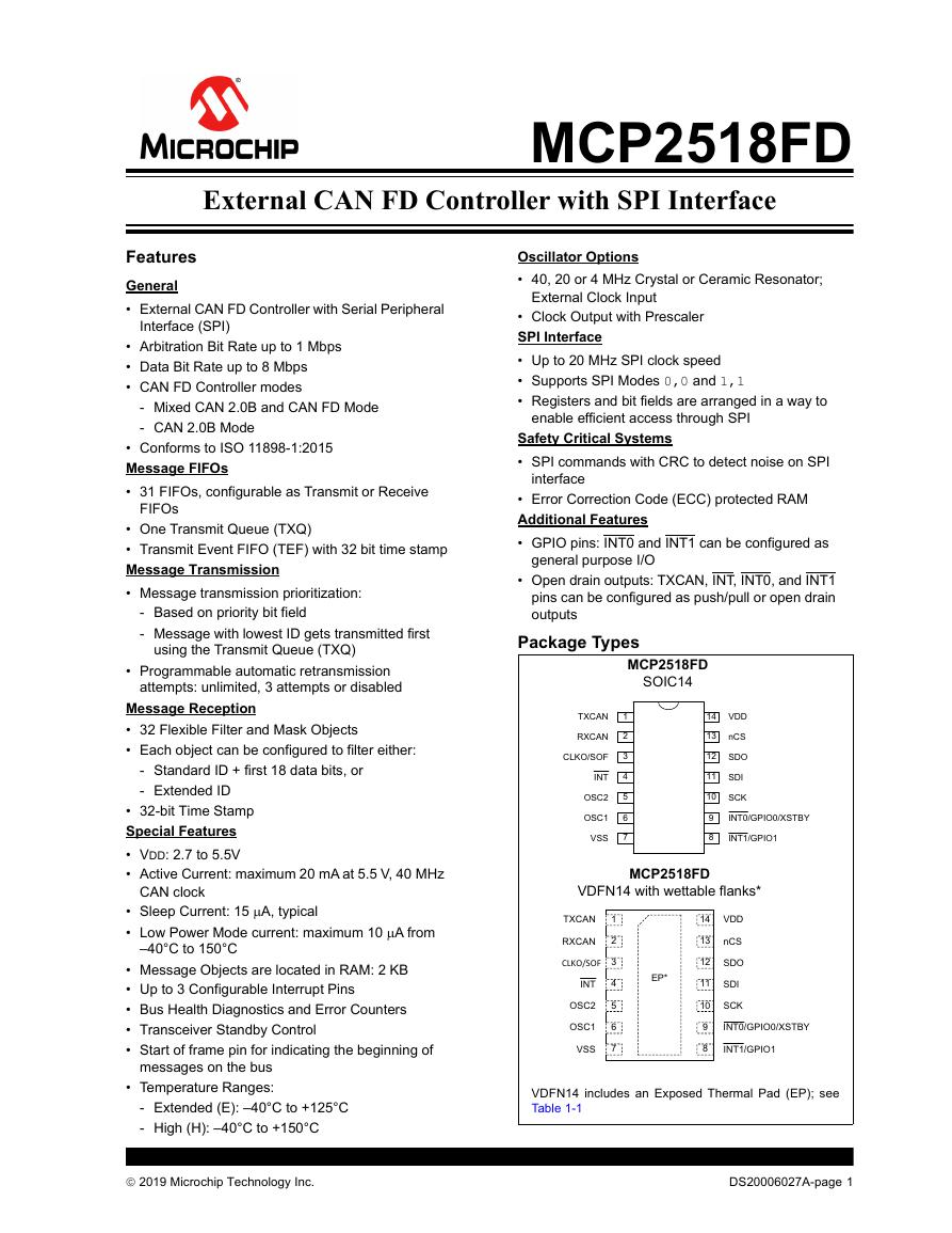
MCP2518FD External CAN FD Controller with SPI Interface Features General • External CAN FD Controller with Serial Peripheral Interface (SPI) • Arbitration Bit Rate up to 1 Mbps • Data Bit Rate up to 8 Mbps • CAN FD Controller modes - Mixed CAN 2.0B and CAN FD Mode - CAN 2.0B Mode • Conforms to ISO 11898-1:2015 Message FIFOs • 31 FIFOs, configurable as Transmit or Receive FIFOs • One Transmit Queue (TXQ) • Transmit Event FIFO (TEF) with 32 bit time stamp Message Transmission • Message transmission prioritization: - Based on priority bit field - Message with lowest ID gets transmitted first using the Transmit Queue (TXQ) • Programmable automatic retransmission attempts: unlimited, 3 attempts or disabled Message Reception • 32 Flexible Filter and Mask Objects • Each object can be configured to filter either: - Standard ID + first 18 data bits, or - Extended ID • 32-bit Time Stamp Special Features • VDD: 2.7 to 5.5V • Active Current: maximum 20 mA at 5.5 V, 40 MHz CAN clock • Sleep Current: 15 A, typical • Low Power Mode current: maximum 10 A from –40°C to 150°C • Message Objects are located in RAM: 2 KB • Up to 3 Configurable Interrupt Pins • Bus Health Diagnostics and Error Counters • Transceiver Standby Control • Start of frame pin for indicating the beginning of messages on the bus • Temperature Ranges: - Extended (E): –40°C to +125°C - High (H): –40°C to +150°C Oscillator Options • 40, 20 or 4 MHz Crystal or Ceramic Resonator; External Clock Input • Clock Output with Prescaler SPI Interface • Up to 20 MHz SPI clock speed • Supports SPI Modes 0,0 and 1,1 • Registers and bit fields are arranged in a way to enable efficient access through SPI Safety Critical Systems • SPI commands with CRC to detect noise on SPI interface • Error Correction Code (ECC) protected RAM Additional Features • GPIO pins: INT0 and INT1 can be configured as general purpose I/O • Open drain outputs: TXCAN, INT, INT0, and INT1 pins can be configured as push/pull or open drain outputs Package Types MCP2518FD SOIC14 TXCAN RXCAN CLKO/SOF INT OSC2 OSC1 VSS 1 2 3 4 5 6 7 14 13 12 11 10 9 8 VDD nCS SDO SDI SCK INT0/GPIO0/XSTBY INT1/GPIO1 MCP2518FD VDFN14 with wettable flanks* TXCAN RXCAN CLKO/SOF INT OSC2 OSC1 VSS 1 2 3 4 5 6 7 EP* 14 13 12 11 10 9 8 VDD nCS SDO SDI SCK INT0/GPIO0/XSTBY INT1/GPIO1 VDFN14 includes an Exposed Thermal Pad (EP); see Table 1-1  2019 Microchip Technology Inc. DS20006027A-page 1
MCP2518FD DEVICE OVERVIEW 1.0 The MCP2518FD device is a cost-effective and small-footprint CAN FD controller that can be easily added to a microcontroller with an available SPI interface. A CAN FD channel can be easily added to a microcontroller that is either lacking a CAN FD peripheral or doesn’t have enough CAN FD channels. MCP2518FD supports both CAN the Classical format (CAN2.0B) and CAN Flexible Data Rate ISO 11898-1:2015. The MCP2518FD device was improved as follows: • Added Low Power Mode (LPM), in order to format, as specified (CAN FD) frames in in reduce leakage current to 10 A over the full temperature range. • Extended SEQ field in Transmit Message Object and Transmit Event FIFO Object from 7 to 23 bits. • Added DEVID register to distinguish between future members of the device family. • Switched to saw cut DFN package with wettable flanks. FIGURE 1-1: MCP2518FD BLOCK DIAGRAM VDD VSS Internal LDO POR SPI Interface Message RAM RAM Controller OSC1 OSC2 Oscillator CAN FD Controller Module I/O RX Filter Block Diagram 1.1 Figure 1.1 shows the block diagram of MCP2518FD device. MCP2518FD contains following main blocks: • The CAN FD Controller module implements the CAN FD protocol, and contains the FIFOs and Filters. the the • The SPI interface is used to control the device by accessing Special Function Registers (SFR) and RAM. • The RAM controller arbitrates the RAM accesses between the SPI and CAN FD Controller module. • The Message RAM is used to store the data of the Message Objects. • The oscillator generates the CAN clock. • The Internal LDO and POR circuit. • The I/O control. Note 1: This data sheet summarizes the features of the MCP2518FD device. It is not intended to be a comprehensive reference source. To complement the information in this data sheet, refer to the related section of the “MCP25xxFD Family Reference Manual”. nCS SCK SDI SDO CLKO/SOF INT INT0/GPIO0/XSTBY INT1/GPIO1 RXCAN TXCAN DS20006027A-page 2  2019 Microchip Technology Inc.
Pinout Description 1.2 Table 1-1 describes the functions of the pins. TABLE 1-1: Pin Name TXCAN RXCAN SOIC VDFN MCP2518FD STANDARD PINOUT VERSION CLKO/SOF INT OSC2 OSC1 VSS INT1/GPIO1 INT0/GPIO0/ XSTBY SCK SDI SDO nCS VDD EP 1 2 3 4 5 6 7 8 9 1 2 3 4 5 6 7 8 9 10 11 12 13 14 - 10 11 12 13 14 15 MCP2518FD Pin Type Description O I O O O I P I/O I/O I I O I P P Transmit output to CAN FD transceiver Receive input from CAN FD transceiver Clock output/Start of Frame output Interrupt output (active low) External oscillator output External oscillator input Ground RX Interrupt output (active low)/GPIO TX Interrupt output (active low)/GPIO/ Transceiver Standby output SPI clock input SPI data input SPI data output SPI chip select input Positive Supply Exposed Pad; connect to VSS Legend: P = Power, I = Input, O = Output  2019 Microchip Technology Inc. DS20006027A-page 3
MCP2518FD Typical Application 1.3 Figure 1-2 shows an example of a typical application of the MCP2518FD device. In this example, the microcontroller operates at 3.3V. interfaces directly with The MCP2518FD device microcontrollers operating at 2.7V to 5.5V. In addition, the MCP2518FD device connects directly to high-speed CAN FD transceivers. There are no external level shifters required when connecting VDD of the MCP2518FD and the microcontroller to VIO of the transceiver. The VDD of the CAN FD transceiver is connected to 5V. The SPI interface is used to configure and control the CAN FD controller. The MCP2518FD device signals interrupts to the microcontroller by using INT, INT0 and INT1. Interrupts need to be cleared by the microcontroller through SPI. The CLKO pin provides the microcontroller. the clock to FIGURE 1-2: MCP2518FD INTERFACING WITH A 3.3V MICROCONTROLLER VBAT 5V LDO 3.3V LDO 0.1uF 0.1uF 0.1uF 0.1uF VDD U C M ® C P I VSS VIO TXD RXD STBY VDD CANH CANL 3 6 5 6 A T A VSS CANH CANL 120 RA0 SCK SDO SDI INT0 INT1 INT2 OSC1 VDD D F 8 1 5 2 P C M TXCAN RXCAN OSC2 nCS SCK SDI SDO INT INT0 INT1 CLKO OSC1 VSS 22pF 22pF DS20006027A-page 4  2019 Microchip Technology Inc.
2.0 CAN FD CONTROLLER MODULE Figure 2-1 shows the main blocks of the CAN FD Controller module: • The CAN FD Controller module has multiple modes: - Configuration - Normal CAN FD - Normal CAN 2.0 - Sleep (normal Sleep mode and Low Power Mode) - Listen Only - Restricted Operation - Internal and External Loop back modes • The CAN FD Bit Stream Processor (BSP) implements the Medium Access Control of the CAN FD protocol described in ISO 11898-1:2015. It serializes and de-serializes the bit stream, encodes and decodes the CAN FD frames, manages the medium access, acknowledges frames and detects and signals errors. • The TX Handler prioritizes the messages that are requested for transmission by the Transmit FIFOs. It uses the RAM Interface to fetch the transmit data from RAM and provides it to the BSP for transmission. • The BSP provides received messages to the RX Handler. The RX Handler uses the Acceptance Filter to filter out messages that shall be stored into Receive FIFOs. It uses the RAM Interface to store received data into RAM. MCP2518FD • Each FIFO can be configured either as a Transmit or Receive FIFO. The FIFO Control keeps track of the FIFO Head and Tail, and calculates the User Address. For a TX FIFO, the User Address points to the address in RAM where the data for the next transmit message shall be stored. For a RX FIFO, the User Address points to the address in RAM where the data of the next receive message shall be read. The User notifies the FIFO that a message was written to or read from RAM by incrementing the Head/Tail of the FIFO. • The Transmit Queue (TXQ) is a special transmit FIFO that transmits the messages based on the ID of the messages stored in the queue. • The Transmit Event FIFO (TEF) stores the message IDs of the transmitted messages. • A free-running Time Base Counter is used to time stamp received messages. Messages in the TEF can also be time stamped. • The CAN FD Controller module generates interrupts when new messages are received or when messages were transmitted successfully. • The SFR are used to control and to read the status of the CAN FD Controller module. Note 1: This data sheet summarizes the features of the CAN FD Controller module. It is not intended to be a comprehensive reference source. To complement the information in this data sheet, refer to the related section of the “MCP25xxFD Family Reference Manual”. FIGURE 2-1: CAN FD CONTROLLER MODULE BLOCK DIAGRAM Mode Control FIFO Control TEF Control SFR Time Stamping TBC RAM Interface TXQ Control TX Handler TX Prioritization Interrupt Control Error Handling Diagnostics RX Handler Acceptance Filter CAN FD Protocol Bit Stream Processor  2019 Microchip Technology Inc. DS20006027A-page 5
MCP2518FD NOTES: DS20006027A-page 6  2019 Microchip Technology Inc.
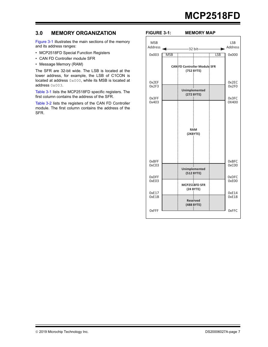
3.0 MEMORY ORGANIZATION Figure 3-1 illustrates the main sections of the memory and its address ranges: • MCP2518FD Special Function Registers • CAN FD Controller module SFR • Message Memory (RAM) The SFR are 32-bit wide. The LSB is located at the lower address, for example, the LSB of C1CON is located at address 0x000, while its MSB is located at address 0x003. Table 3-1 lists the MCP2518FD specific registers. The first column contains the address of the SFR. Table 3-2 lists the registers of the CAN FD Controller module. The first column contains the address of the SFR. MCP2518FD FIGURE 3-1: MEMORY MAP MSB Address 0x003 MSB 32 bit LSB Address LSB 0x000 CAN FD Controller Module SFR (752 BYTE) 0x2EF 0x2F3 0x3FF 304x0 0xBFF 0xC03 0xDFF 0xE03 0xE17 0xE1B 0xFFF Unimplemented (272 BYTE) RAM (2KBYTE) Unimplemented (512 BYTE) MCP2518FD SFR (24 BYTE) Reserved (488 BYTE) 0x2EC 0x2F0 0x3FC 004X0 0xBFC 0xC00 0xDFC 0xE00 0xE14 0xE18 0xFFC  2019 Microchip Technology Inc. DS20006027A-page 7
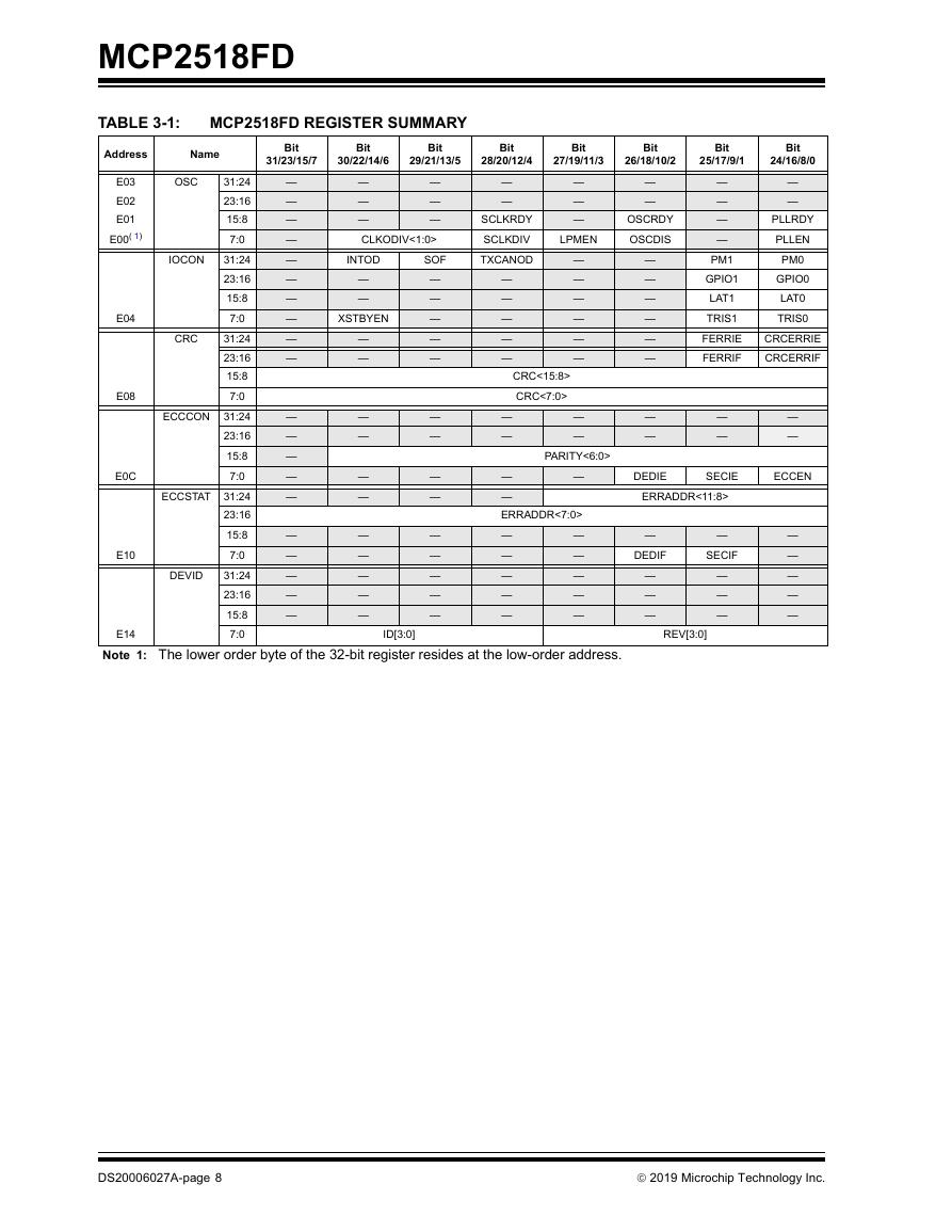
MCP2518FD TABLE 3-1: MCP2518FD REGISTER SUMMARY Address Name Bit 31/23/15/7 Bit 30/22/14/6 Bit 29/21/13/5 Bit 28/20/12/4 Bit 27/19/11/3 Bit 26/18/10/2 Bit 25/17/9/1 Bit 24/16/8/0 E03 E02 E01 E00( 1) E04 E08 E0C E10 E14 OSC CRC IOCON 31:24 23:16 15:8 7:0 31:24 23:16 15:8 7:0 31:24 23:16 15:8 7:0 ECCCON 31:24 23:16 15:8 7:0 ECCSTAT 31:24 23:16 15:8 7:0 31:24 23:16 15:8 7:0 DEVID — — — — — — — — — — — — — — — — — — — — — — — — — — CLKODIV<1:0> INTOD — — XSTBYEN — — — — — — — — — — — SOF — — — — — — — — — — — — — — — — SCLKRDY SCLKDIV TXCANOD — — — LPMEN — — OSCRDY OSCDIS — — — — — — — CRC<15:8> CRC<7:0> — — — — — — — — — — — — — — — — — — — — PM1 GPIO1 LAT1 TRIS1 FERRIE FERRIF — — PLLRDY PLLEN PM0 GPIO0 LAT0 TRIS0 CRCERRIE CRCERRIF — — — — PARITY<6:0> — — — ERRADDR<7:0> — — — — — — — — — — DEDIE SECIE ECCEN ERRADDR<11:8> — DEDIF — — — — SECIF — — — — — — — — ID[3:0] REV[3:0] Note 1: The lower order byte of the 32-bit register resides at the low-order address. DS20006027A-page 8  2019 Microchip Technology Inc.
分享到:
收藏