LM193, LM293, LM293A, LM393, LM393A, LM2903, LM2903V
SLCS005Y –OCTOBER 1979–REVISED JUNE 2015
LMx93, LM2903 Dual Differential Comparators
3 Description
These devices consist of
two independent voltage
comparators that are designed to operate from a
single power supply over a wide range of voltages.
Operation from dual supplies also is possible as long
as the difference between the two supplies is 2 V to
36 V, and VCC is at least 1.5 V more positive than the
input
common-mode voltage. Current drain is
independent of the supply voltage. The outputs can
be connected to other open-collector outputs to
achieve wired-AND relationships.
The LM193 device is characterized for operation from
−55°C to 125°C. The LM293 and LM293A devices
are characterized for operation from −25°C to 85°C.
The LM393 and LM393A devices are characterized
for operation from 0°C to 70°C. The LM2903 device
is characterized for operation from −40°C to 125°C.
Device Information(1)
1 Features
1• Single-Supply or Dual Supplies
• Wide Range of Supply Voltage
•
– Maximum Rating: 2 V to 36 V
– Tested to 30 V: Non-V Devices
– Tested to 32 V: V-Suffix Devices
Low Supply-Current Drain Independent of Supply
Voltage: 0.4 mA (Typical) Per Comparator
Low Input Bias Current: 25 nA (Typical)
Low Input Offset Current: 3 nA (Typical) (LM139)
Low Input Offset Voltage: 2 mV (Typical)
•
•
•
• Common-Mode Input Voltage Range
Includes Ground
• Differential Input Voltage Range Equal to
Maximum-Rated Supply Voltage: ±36 V
Low Output Saturation Voltage
•
• Output Compatible With TTL, MOS, and CMOS
• On Products Compliant to MIL-PRF-38535,
All Parameters Are Tested Unless Otherwise
Noted. On All Other Products, Production
Processing Does Not Necessarily Include Testing
of All Parameters.
2 Applications
• Chemical or Gas Sensor
• Desktop PC
• Motor Control: AC Induction
• Weigh Scale
4.90 mm x 6.00 mm
VSSOP (8)
3.00 mm x 5.00 mm
PACKAGE
BODY SIZE (NOM)
PART NUMBER
LM193D, LM293D,
LM293AD, LM393D, SOIC (8)
LM393AD,
LM2903D
LM293DGK,
LM293ADGK,
LM393DGK,
LM393ADGK,
LM2903DGK
LM293P, LM393P,
LM393AP,
LM2903P
LM393PS,
LM393APS,
LM2903PS
LM393PW,
LM393APW,
LM2903PW
LM193JG
LM193FK
(1) For all available packages, see the orderable addendum at
10.00 mm x 7.00 mm
9.00 mm x 9.00 mm
GDIP (8)
CQCC (8)
9.50 mm × 6.30 mm
TSSOP (8)
6.40 mm x 3.00 mm
PDIP (8)
SO (8)
6.20 mm x 7.90 mm
the end of the data sheet.
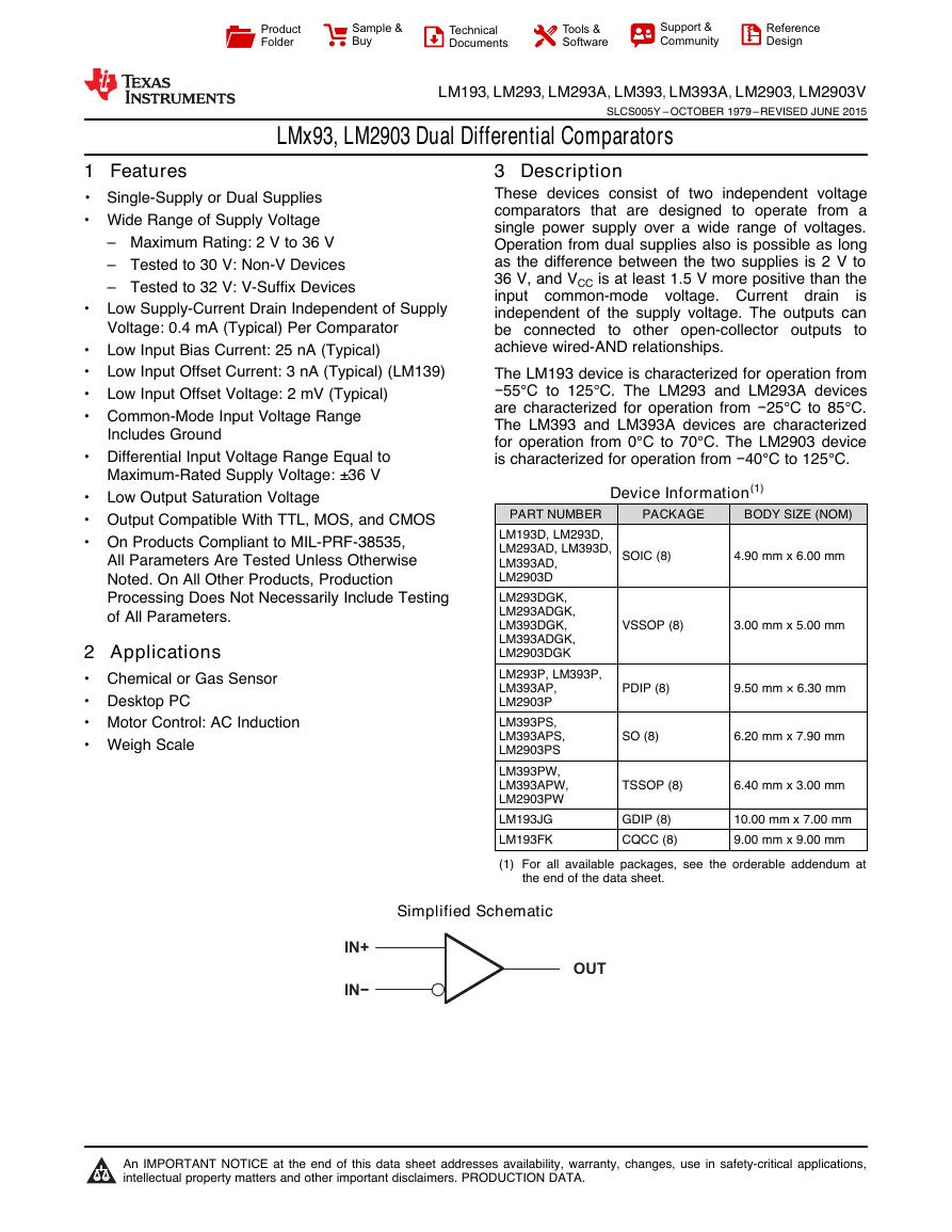
Simplified Schematic
1
An IMPORTANT NOTICE at the end of this data sheet addresses availability, warranty, changes, use in safety-critical applications,
intellectual property matters and other important disclaimers. PRODUCTION DATA.
OUTIN−IN+ProductFolderSample &BuyTechnicalDocumentsTools &SoftwareSupport &CommunityReferenceDesign�
LM193, LM293, LM293A, LM393, LM393A, LM2903, LM2903V
SLCS005Y –OCTOBER 1979–REVISED JUNE 2015
www.ti.com
Table of Contents
1
Features.................................................................. 1
2 Applications ........................................................... 1
3 Description ............................................................. 1
4 Revision History..................................................... 2
5 Pin Configuration and Functions ......................... 3
6 Specifications......................................................... 4
6.1 Absolute Maximum Ratings ...................................... 4
6.2 ESD Ratings.............................................................. 4
6.3 Recommended Operating Conditions....................... 4
6.4 Thermal Information.................................................. 4
6.5 Electrical Characteristics for LMx93.......................... 5
6.6 Electrical Characteristics for LMx93A ....................... 6
6.7 Electrical Characteristics for LM2903 and LM2903A 7
6.8 Switching Characteristics.......................................... 7
6.9 Typical Characteristics.............................................. 8
7 Detailed Description .............................................. 9
7.1 Overview ................................................................... 9
7.2 Functional Block Diagram ......................................... 9
7.3 Feature Description................................................... 9
7.4 Device Functional Modes.......................................... 9
8 Application and Implementation ........................ 10
8.1 Application Information............................................ 10
8.2 Typical Application ................................................. 10
9 Power Supply Recommendations...................... 12
10 Layout................................................................... 12
10.1 Layout Guidelines ................................................. 12
10.2 Layout Example .................................................... 12
11 Device and Documentation Support ................. 13
11.1 Related Links ........................................................ 13
11.2 Community Resources.......................................... 13
11.3 Trademarks ........................................................... 13
11.4 Electrostatic Discharge Caution............................ 13
11.5 Glossary ................................................................ 13
12 Mechanical, Packaging, and Orderable
Information ........................................................... 13
4 Revision History
NOTE: Page numbers for previous revisions may differ from page numbers in the current version.
Changes from Revision X (January 2014) to Revision Y
Page
• Added ESD Ratings table, Feature Description section, Device Functional Modes, Application and Implementation
section, Power Supply Recommendations section, Layout section, Device and Documentation Support section, and
Mechanical, Packaging, and Orderable Information section. ................................................................................................ 1
Changes from Revision W (July 2010) to Revision X
Page
• Updated document to new TI data sheet format - no specification changes. ........................................................................ 1
• Updated Features................................................................................................................................................................... 1
• Removed Ordering Information table ..................................................................................................................................... 3
• Added ESD warning. ............................................................................................................................................................ 13
2
Submit Documentation Feedback
Copyright © 1979–2015, Texas Instruments Incorporated
Product Folder Links: LM193 LM293 LM293A LM393 LM393A LM2903 LM2903V
�
www.ti.com
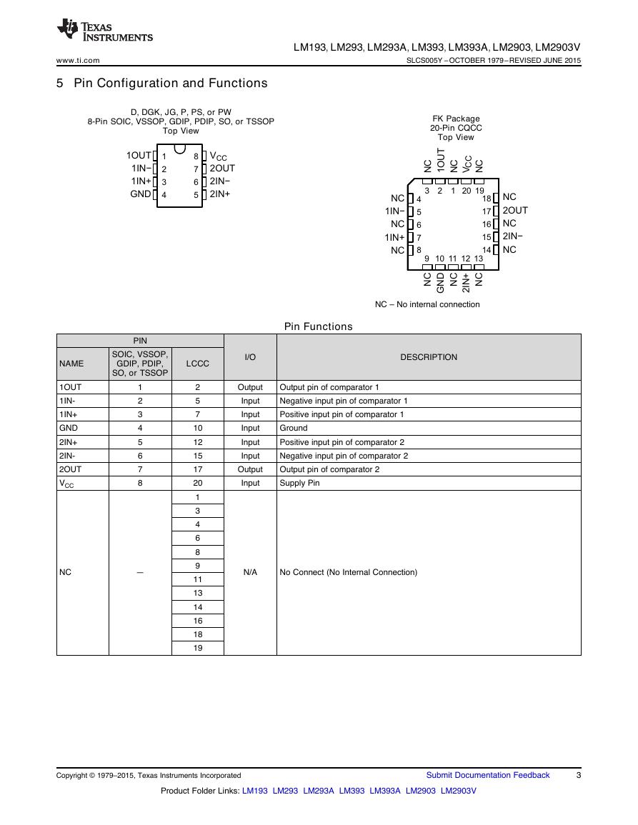
5 Pin Configuration and Functions
LM193, LM293, LM293A, LM393, LM393A, LM2903, LM2903V
SLCS005Y –OCTOBER 1979–REVISED JUNE 2015
D, DGK, JG, P, PS, or PW
8-Pin SOIC, VSSOP, GDIP, PDIP, SO, or TSSOP
Top View
FK Package
20-Pin CQCC
Top View
NC – No internal connection
Pin Functions
DESCRIPTION
Output pin of comparator 1
Negative input pin of comparator 1
Positive input pin of comparator 1
Ground
Positive input pin of comparator 2
Negative input pin of comparator 2
Output pin of comparator 2
Supply Pin
I/O
Output
Input
Input
Input
Input
Input
Output
Input
N/A
No Connect (No Internal Connection)
NAME
1OUT
1IN-
1IN+
GND
2IN+
2IN-
2OUT
VCC
1
2
3
4
5
6
7
8
NC
—
PIN
SOIC, VSSOP,
GDIP, PDIP,
SO, or TSSOP
LCCC
2
5
7
10
12
15
17
20
1
3
4
6
8
9
11
13
14
16
18
19
Copyright © 1979–2015, Texas Instruments Incorporated
Submit Documentation Feedback
3
Product Folder Links: LM193 LM293 LM293A LM393 LM393A LM2903 LM2903V
3212019910111213456781817161514NC2OUTNC2IN−NCNC1IN−NC1IN+NCNC1OUTNC2IN+NCVNCNCGNDNCCC123487651OUT1IN−1IN+GNDVCC2OUT2IN−2IN+�
LM193, LM293, LM293A, LM393, LM393A, LM2903, LM2903V
SLCS005Y –OCTOBER 1979–REVISED JUNE 2015
6 Specifications
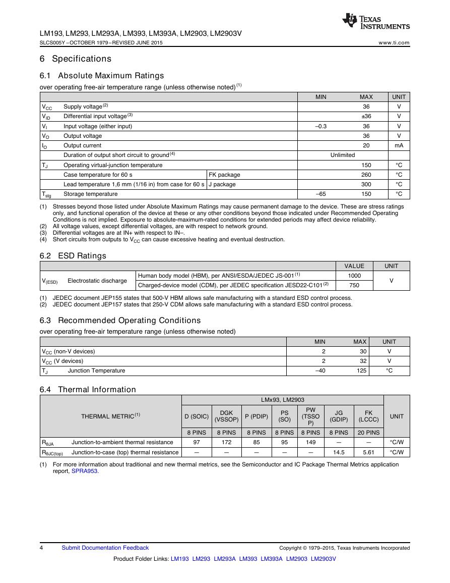
6.1 Absolute Maximum Ratings
over operating free-air temperature range (unless otherwise noted)(1)
VCC
VID
VI
VO
IO
TJ
Supply voltage(2)
Differential input voltage(3)
Input voltage (either input)
Output voltage
Output current
Duration of output short circuit to ground(4)
Operating virtual-junction temperature
Case temperature for 60 s
Lead temperature 1,6 mm (1/16 in) from case for 60 s J package
Storage temperature
FK package
www.ti.com
MIN
–0.3
Unlimited
MAX
36
±36
36
36
20
UNIT
V
V
V
V
mA
150
260
300
150
°C
°C
°C
°C
Tstg
(1) Stresses beyond those listed under Absolute Maximum Ratings may cause permanent damage to the device. These are stress ratings
only, and functional operation of the device at these or any other conditions beyond those indicated under Recommended Operating
Conditions is not implied. Exposure to absolute-maximum-rated conditions for extended periods may affect device reliability.
–65
(2) All voltage values, except differential voltages, are with respect to network ground.
(3) Differential voltages are at IN+ with respect to IN–.
(4) Short circuits from outputs to VCC can cause excessive heating and eventual destruction.
6.2 ESD Ratings
V(ESD)
Electrostatic discharge
Human body model (HBM), per ANSI/ESDA/JEDEC JS-001(1)
Charged-device model (CDM), per JEDEC specification JESD22-C101(2)
VALUE
1000
750
UNIT
V
(1)
(2)
JEDEC document JEP155 states that 500-V HBM allows safe manufacturing with a standard ESD control process.
JEDEC document JEP157 states that 250-V CDM allows safe manufacturing with a standard ESD control process.
6.3 Recommended Operating Conditions
over operating free-air temperature range (unless otherwise noted)
VCC (non-V devices)
VCC (V devices)
TJ
Junction Temperature
6.4 Thermal Information
MIN
2
2
–40
MAX
30
32
125
UNIT
V
V
°C
LMx93, LM2903
THERMAL METRIC(1)
D (SOIC)
DGK
(VSSOP)
P (PDIP)
PS
(SO)
PW
(TSSO
P)
JG
(GDIP)
FK
(LCCC)
UNIT
8 PINS
8 PINS
8 PINS
8 PINS 8 PINS
8 PINS
20 PINS
Junction-to-ambient thermal resistance
Junction-to-case (top) thermal resistance
RθJA
RθJC(top)
(1) For more information about traditional and new thermal metrics, see the Semiconductor and IC Package Thermal Metrics application
—
14.5
—
5.61
172
—
149
—
97
—
85
—
95
—
°C/W
°C/W
report, SPRA953.
4
Submit Documentation Feedback
Copyright © 1979–2015, Texas Instruments Incorporated
Product Folder Links: LM193 LM293 LM293A LM393 LM393A LM2903 LM2903V
�
www.ti.com
LM193, LM293, LM293A, LM393, LM393A, LM2903, LM2903V
SLCS005Y –OCTOBER 1979–REVISED JUNE 2015
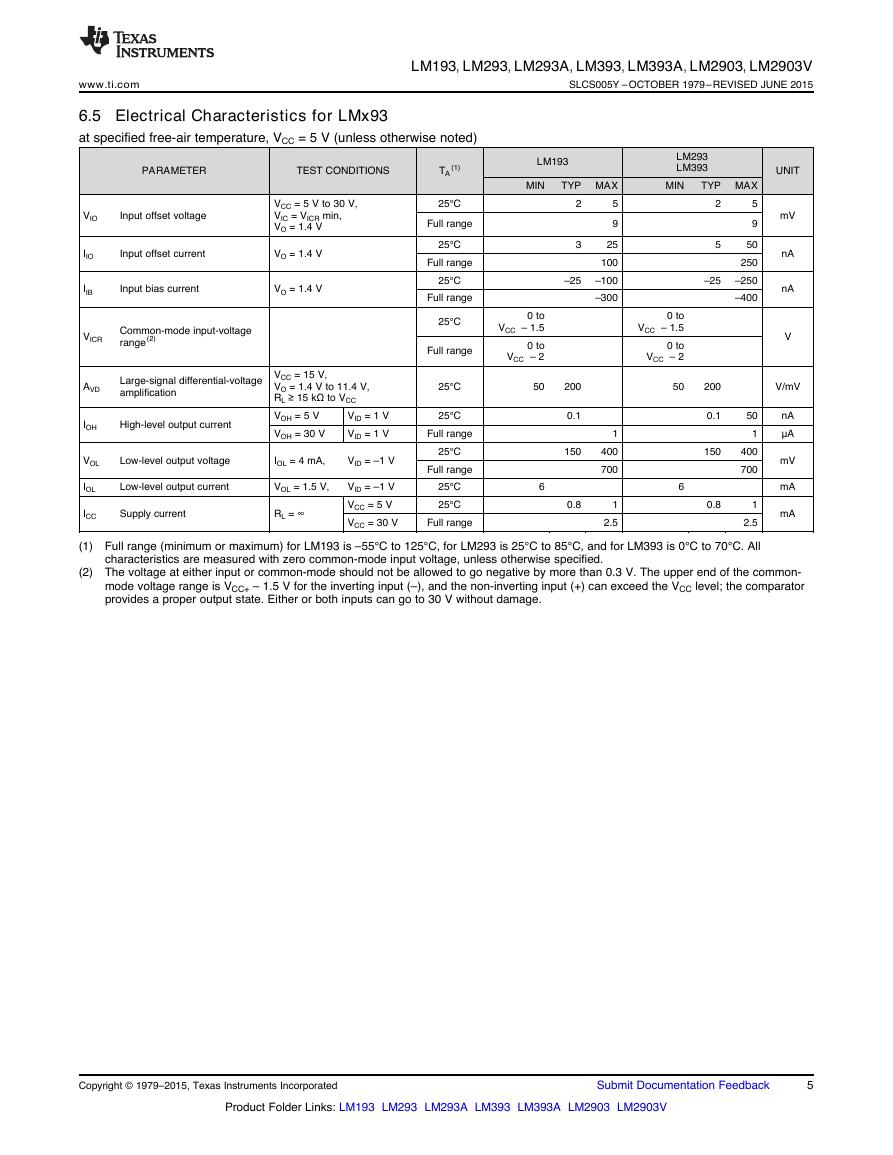
6.5 Electrical Characteristics for LMx93
at specified free-air temperature, VCC = 5 V (unless otherwise noted)
PARAMETER
TEST CONDITIONS
VIO
Input offset voltage
IIO
IIB
Input offset current
Input bias current
VCC = 5 V to 30 V,
VIC = VICR min,
VO = 1.4 V
VO = 1.4 V
VO = 1.4 V
VICR
Common-mode input-voltage
range(2)
AVD
IOH
VOL
IOL
ICC
Large-signal differential-voltage
amplification
High-level output current
VCC = 15 V,
VO = 1.4 V to 11.4 V,
RL ≥ 15 kΩ to VCC
VOH = 5 V
VOH = 30 V
VID = 1 V
VID = 1 V
Low-level output voltage
IOL = 4 mA,
VID = –1 V
Low-level output current
VOL = 1.5 V,
Supply current
RL = ∞
VID = –1 V
VCC = 5 V
VCC = 30 V
(1)
TA
25°C
Full range
25°C
Full range
25°C
Full range
25°C
Full range
25°C
25°C
Full range
25°C
Full range
25°C
25°C
Full range
LM193
LM293
LM393
MIN
TYP MAX
5
2
MIN
TYP MAX
5
2
3
–25
9
25
100
–100
–300
5
–25
9
50
250
–250
–400
0 to
VCC – 1.5
0 to
VCC – 2
0 to
VCC – 1.5
0 to
VCC – 2
UNIT
mV
nA
nA
V
50
200
50
200
V/mV
0.1
150
0.8
6
1
400
700
1
2.5
0.1
150
0.8
6
50
1
400
700
1
2.5
nA
μA
mV
mA
mA
(1) Full range (minimum or maximum) for LM193 is –55°C to 125°C, for LM293 is 25°C to 85°C, and for LM393 is 0°C to 70°C. All
characteristics are measured with zero common-mode input voltage, unless otherwise specified.
(2) The voltage at either input or common-mode should not be allowed to go negative by more than 0.3 V. The upper end of the common-
mode voltage range is VCC+ – 1.5 V for the inverting input (–), and the non-inverting input (+) can exceed the VCC level; the comparator
provides a proper output state. Either or both inputs can go to 30 V without damage.
Copyright © 1979–2015, Texas Instruments Incorporated
Submit Documentation Feedback
5
Product Folder Links: LM193 LM293 LM293A LM393 LM393A LM2903 LM2903V
�
LM193, LM293, LM293A, LM393, LM393A, LM2903, LM2903V
SLCS005Y –OCTOBER 1979–REVISED JUNE 2015
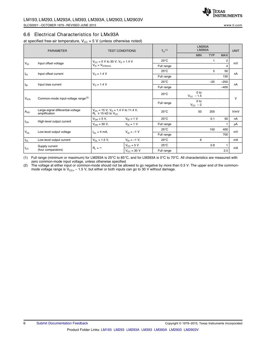
6.6 Electrical Characteristics for LMx93A
at specified free-air temperature, VCC = 5 V (unless otherwise noted)
PARAMETER
TEST CONDITIONS
VIO
IIO
IIB
Input offset voltage
Input offset current
Input bias current
VCC = 5 V to 30 V, VO = 1.4 V
VIC = VICR(min)
VO = 1.4 V
VO = 1.4 V
VICR
Common-mode input-voltage range(2)
AVD
IOH
VOL
IOL
ICC
Large-signal differential-voltage
amplification
High-level output current
VCC = 15 V, VO = 1.4 V to 11.4 V,
RL ≥ 15 kΩ to VCC
VOH = 5 V,
VOH = 30 V,
VID = 1 V
VID = 1 V
Low-level output voltage
Low-level output current
Supply current
(four comparators)
IOL = 4 mA,
VOL = 1.5 V,
RL = ∞
VID = –1 V
VID = –1 V,
VCC = 5 V
VCC = 30 V
(1)
TA
25°C
Full range
25°C
Full range
25°C
Full range
25°C
Full range
25°C
25°C
Full range
25°C
Full range
25°C
25°C
Full range
www.ti.com
TYP
1
5
–25
200
0.1
150
0.8
UNIT
mV
nA
nA
V
V/mV
nA
μA
mV
mA
mA
MAX
2
4
50
150
–250
–400
50
1
400
700
1
2.5
LM293A
LM393A
MIN
0 to
VCC – 1.5
0 to
VCC – 2
50
6
(1) Full range (minimum or maximum) for LM293A is 25°C to 85°C, and for LM393A is 0°C to 70°C. All characteristics are measured with
zero common-mode input voltage, unless otherwise specified.
(2) The voltage at either input or common-mode should not be allowed to go negative by more than 0.3 V. The upper end of the common-
mode voltage range is VCC+ – 1.5 V, but either or both inputs can go to 30 V without damage.
6
Submit Documentation Feedback
Copyright © 1979–2015, Texas Instruments Incorporated
Product Folder Links: LM193 LM293 LM293A LM393 LM393A LM2903 LM2903V
�
www.ti.com
LM193, LM293, LM293A, LM393, LM393A, LM2903, LM2903V
SLCS005Y –OCTOBER 1979–REVISED JUNE 2015
6.7 Electrical Characteristics for LM2903 and LM2903A
at specified free-air temperature, VCC = 5 V (unless otherwise noted)
(1)
TEST CONDITIONS
PARAMETER
TA
VIO
Input offset voltage
VCC = 5 V to MAX(2) ,
VO = 1.4 V,
VIC = VICR(min),
IIO
IIB
Input offset current
VO = 1.4 V
Input bias current
VO = 1.4 V
VICR
Common-mode input-
voltage range(3)
AVD
IOH
VOL
IOL
ICC
Large-signal differential-
voltage amplification
High-level output current
VCC = 15 V, VO = 1.4 V to 11.4 V,
RL ≥ 15 kΩ to VCC
VOH = 5 V,
VOH = VCC MAX(2),
VID = 1 V
VID = 1 V
Low-level output voltage
IOL = 4 mA,
Low-level output current
VOL = 1.5 V,
Supply current
RL = ∞
VID = –1 V,
VID = –1 V
VCC = 5 V
VCC = MAX
25°C
Full range
25°C
Full range
25°C
Full range
25°C
Full range
25°C
25°C
Full range
25°C
Full range
25°C
25°C
Full range
LM2903
MIN
TYP MAX
7
2
LM2903A
MIN
TYP MAX
2
1
5
–25
100
0.1
150
0.8
15
50
200
–250
–500
50
1
400
700
1
2.5
0 to
VCC – 1.5
0 to
VCC – 2
25
6
5
–25
100
0.1
150
0.8
4
50
200
–250
–500
50
1
400
700
1
2.5
0 to
VCC – 1.5
0 to
VCC – 2
25
6
UNIT
mV
nA
nA
V
V/mV
nA
μA
mV
mA
mA
(1) Full range (minimum or maximum) for LM2903 is –40°C to 125°C. All characteristics are measured with zero common-mode input
voltage, unless otherwise specified.
(2) VCC MAX = 30 V for non-V devices and 32 V for V-suffix devices.
(3) The voltage at either input or common-mode should not be allowed to go negative by more than 0.3 V. The upper end of the common-
mode voltage range is VCC+ – 1.5 V, but either or both inputs can go to 30 V (32 V for V-suffix devices) without damage.
6.8 Switching Characteristics
VCC = 5 V, TA = 25°C
PARAMETER
TEST CONDITIONS
Response time
RL connected to 5 V through 5.1 kΩ,
CL = 15 pF(1)(2)
100-mV input step with 5-mV overdrive
TTL-level input step
LM2901, LM293, LM293A
LM393, LM393A LM2903
TYP
1.3
0.3
UNIT
μs
(1) CL includes probe and jig capacitance.
(2) The response time specified is the interval between the input step function and the instant when the output crosses 1.4 V.
Copyright © 1979–2015, Texas Instruments Incorporated
Submit Documentation Feedback
7
Product Folder Links: LM193 LM293 LM293A LM393 LM393A LM2903 LM2903V
�
LM193, LM293, LM293A, LM393, LM393A, LM2903, LM2903V
SLCS005Y –OCTOBER 1979–REVISED JUNE 2015
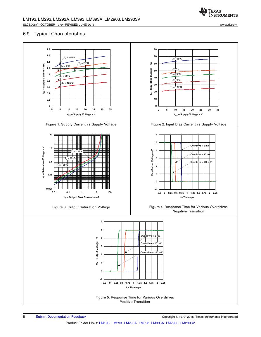
6.9 Typical Characteristics
www.ti.com
Figure 1. Supply Current vs Supply Voltage
Figure 2. Input Bias Current vs Supply Voltage
Figure 3. Output Saturation Voltage
Figure 4. Response Time for Various Overdrives
Negative Transition
Figure 5. Response Time for Various Overdrives
Positive Transition
8
Submit Documentation Feedback
Copyright © 1979–2015, Texas Instruments Incorporated
Product Folder Links: LM193 LM293 LM293A LM393 LM393A LM2903 LM2903V
-10123456-0.300.250.50.7511.251.51.7522.25t–Time–µsVO–OutputVoltage–VOverdrive = 5 mVOverdrive = 100 mVOverdrive = 20 mV0.0010.010.11100.010.1110100IO–OutputSinkCurrent–mAVO–SaturationVoltage–VT= –55°CAT= 25°CAT= 125°CA-10123456-0.300.250.50.7511.251.51.7522.25t–Time–µsVO–OutputVoltage–VOverdrive = 5 mVOverdrive = 100 mVOverdrive = 20 mV00.20.40.60.811.21.41.61.805101520253035VCC–SupplyVoltage–VICC–SupplyCurrent–mAT= –55°CAT= 0°CAT= 25°CAT= 70°CAT= 125°CA0102030405060708005101520253035VCC–SupplyVoltage–VIIN–InputBiasCurrent–nAT= –55°CAT= 0°CAT= 25°CAT= 70°CAT= 125°CA�



 V2版本原理图(Capacitive-Fingerprint-Reader-Schematic_V2).pdf
 摄像头工作原理.doc
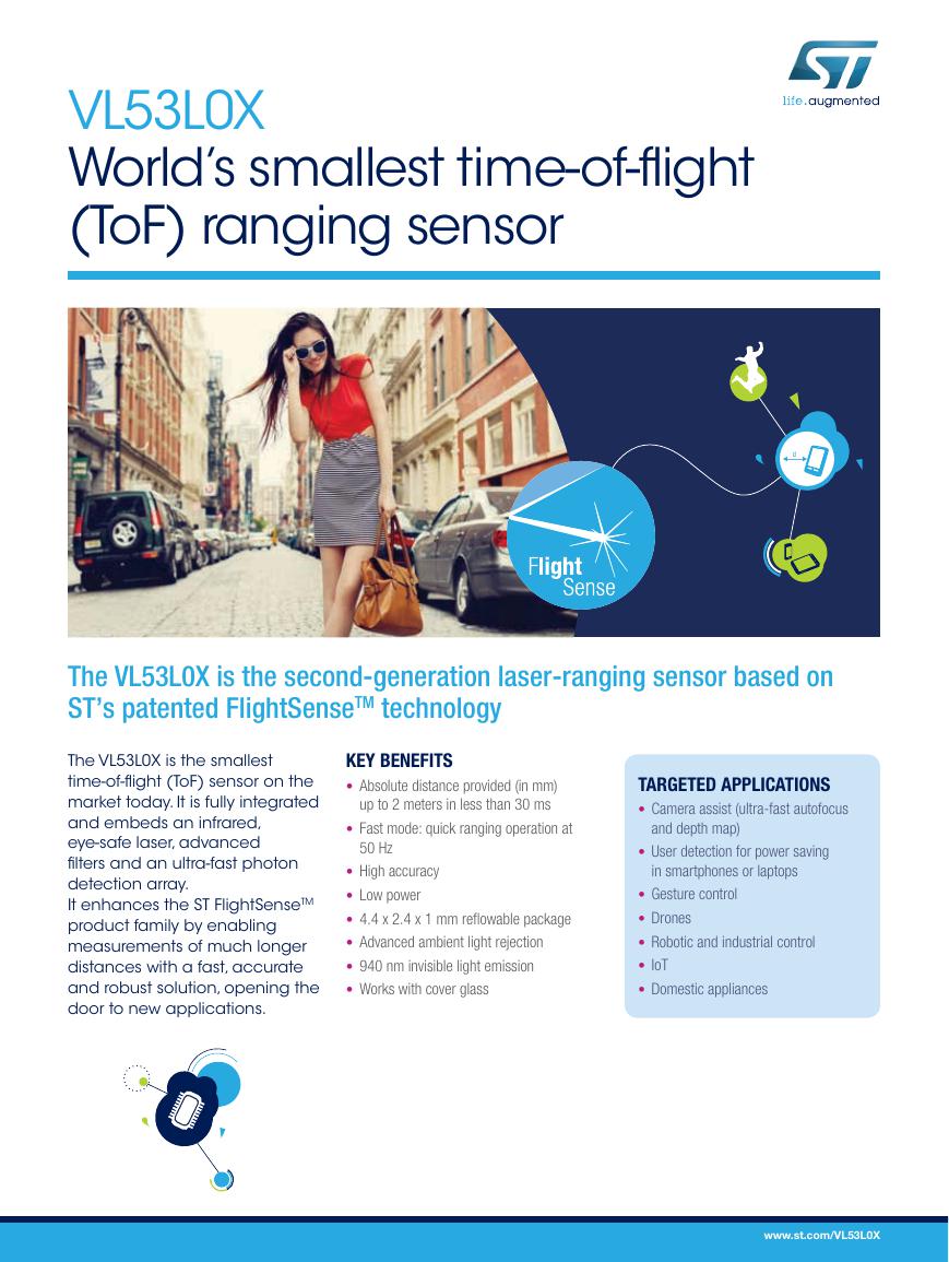 VL53L0X简要说明(En.FLVL53L00216).pdf
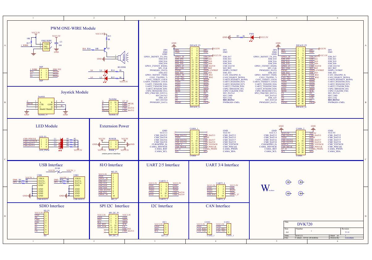 原理图(DVK720-Schematic).pdf
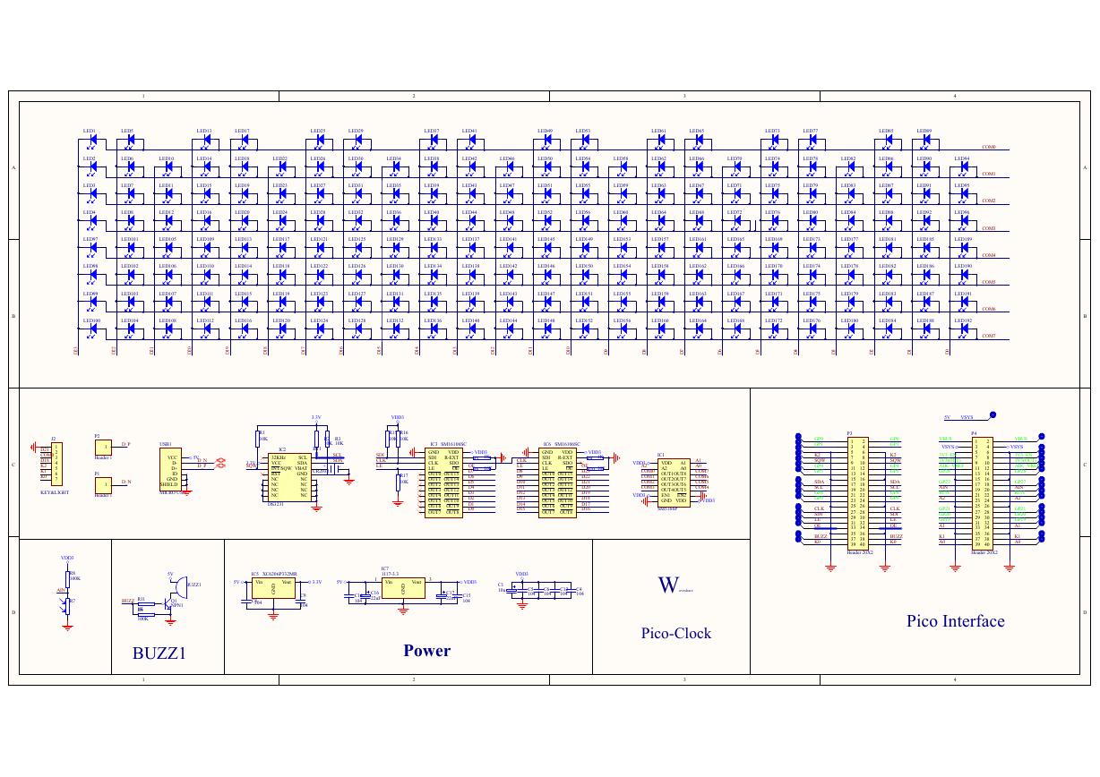 原理图(Pico-Clock-Green-Schdoc).pdf
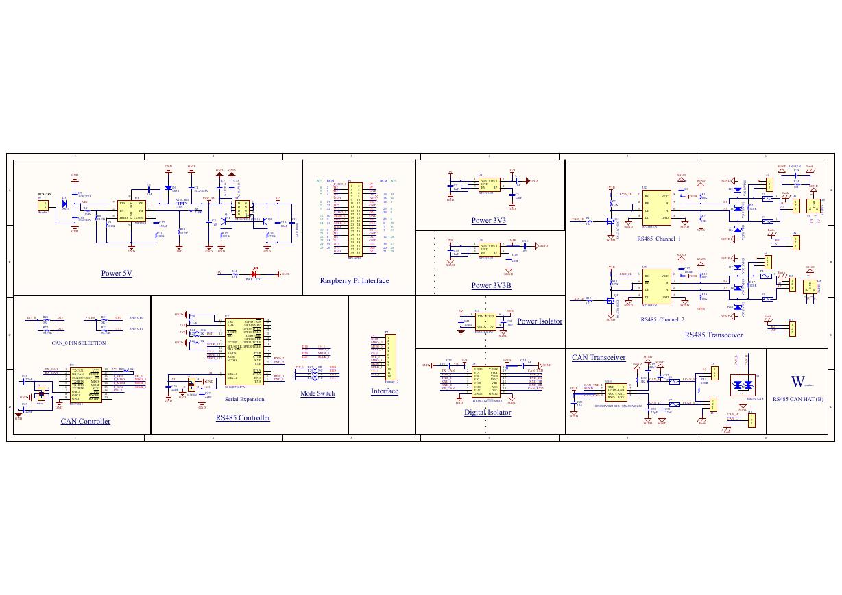 原理图(RS485-CAN-HAT-B-schematic).pdf
 File:SIM7500_SIM7600_SIM7800 Series_SSL_Application Note_V2.00.pdf
 ADS1263(Ads1262).pdf
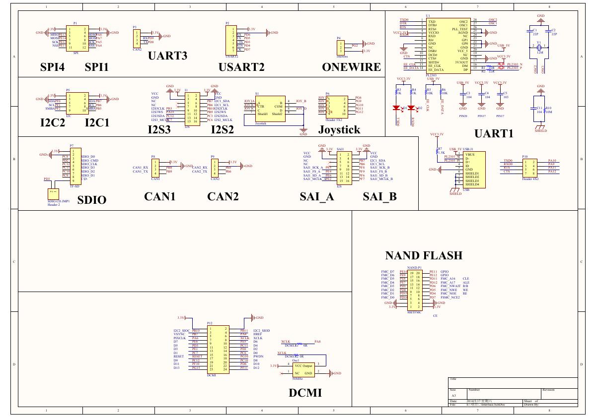 原理图(Open429Z-D-Schematic).pdf
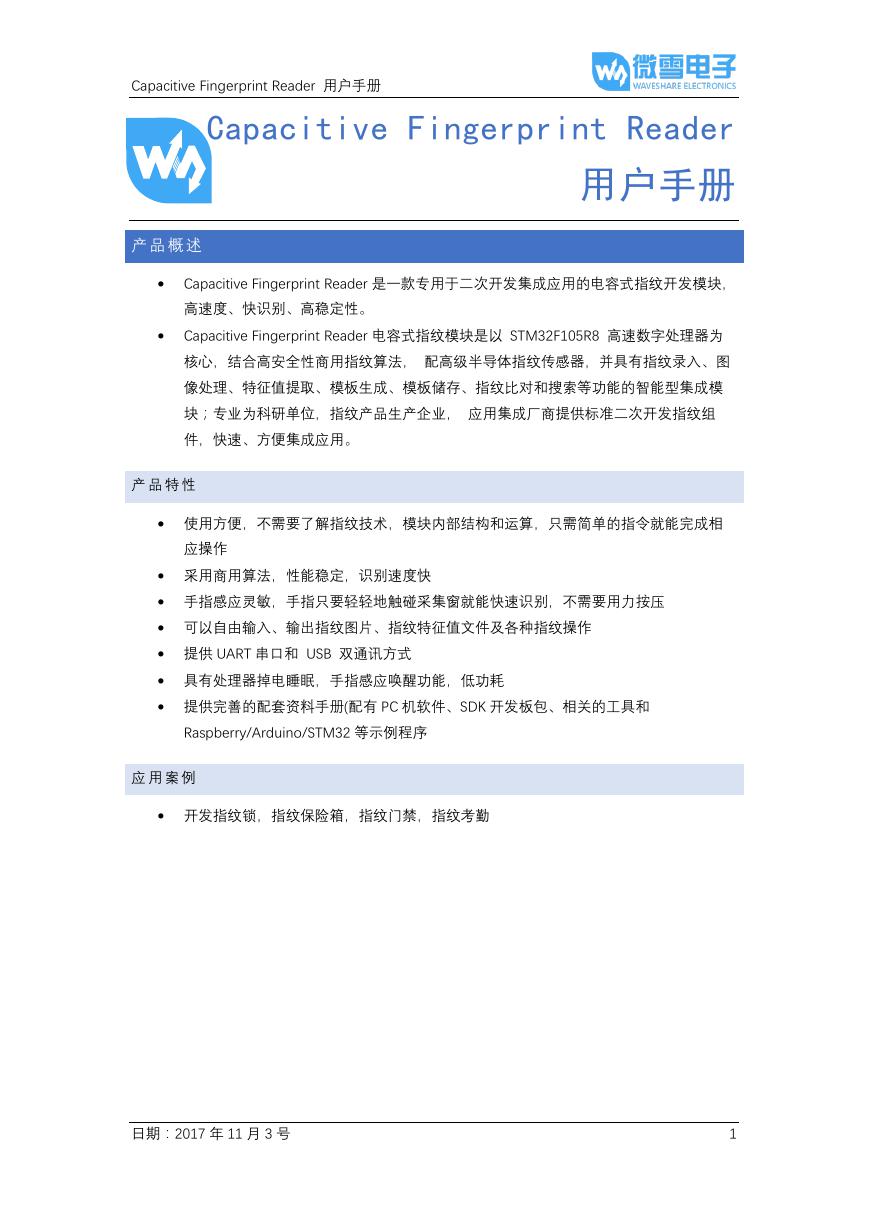 用户手册(Capacitive_Fingerprint_Reader_User_Manual_CN).pdf
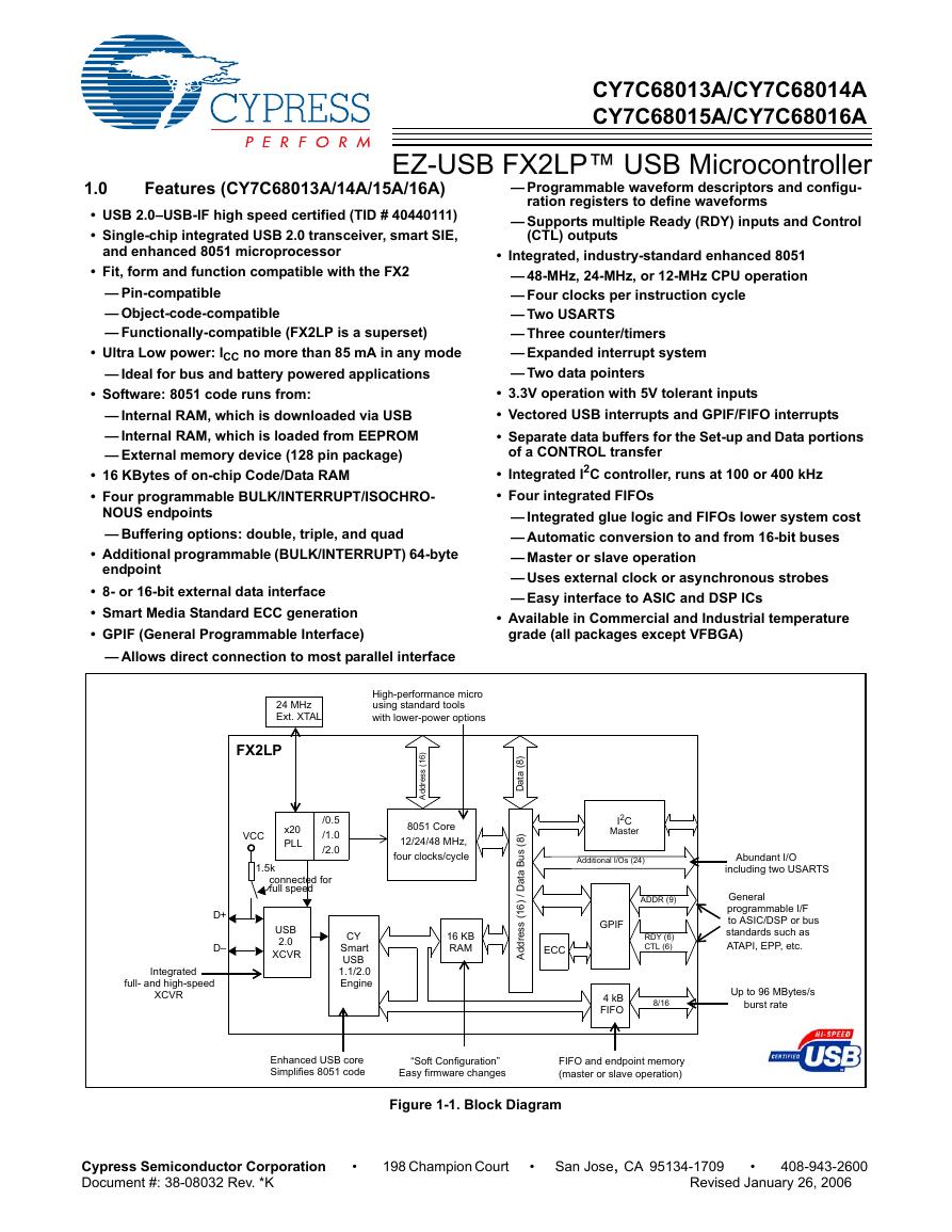 CY7C68013A(英文版)(CY7C68013A).pdf
 TechnicalReference_Dem.pdf