IP5306
Fully-Integrated Power Bank System-On-Chip with
2.1A charger, 2.4A discharger
Features
Applications
Switch buck charger and boost
2.1A Synchronous switching charger and 5V
2.4A boost converter
Boost converter efficiency up to 92%
Switching charger efficiency up to 91%
Integrated power-path management,
charging batteries and charging cellphones
at the same time
Charger
Adaptive charging current control, excellent
adapter compatibility
Support 4.20/4.30/4.35/4.40V batteries
State of charge (SOC) indicator
Integrated LED controller supports 4/3/2/1
LEDs as the SOC indicator
Fully featured
Key ON/OFF
Integrated flashlight controller
Integrated cellphone plug-in and plug-out
detector
Low power
Smart load detector, switching to standby
mode automatically
<100 µA standby current
Ultra simplified BOM
Integrated power FET, charging/boosting
with a single inductor
Multiple protections, high reliability
Output over-current, over-voltage,
short-circuit protection
Input over-voltage, over-current, battery
over-charge, over-drain, over-current
protection
Thermal Shutdown
ESD 4KV
Power bank, Portable Charger
Mobile Phones, Smart Phones, Handheld
Devices, Portable Media Player, Tablet
Description
IP5306 is a fully-integrated multi-function
power management SoC. It integrates a boost
converter, a Li battery charger management
system and a battery state of charge indicate
controller. It provides a turn-key solution for power
bank and portable charger applications.
IP5306’s high integration and rich features
make the minimized component number in
application. It can effectively downsize the
application and lower the BOM cost.
IP5306 only needs a single inductor to realize
step-down and step-up which provides 2.4A
output current. It can switch to standby mode at
light load automatically
IP5306’s synchronous switching charger
provides 2A charging current. Its efficiency is up to
91%. It regulates the charging current by IC
temperature and input voltage.。
IP5306 integrates voltage based fuel gauge
indication of 1/2/3/4 LEDs and flashlight function.
IP5306 is available in ESOP8
V1.31 http://www.injoinic.com/ 1 / 11 Copyright © 2016, Injoinic Corp.
�
IP5306
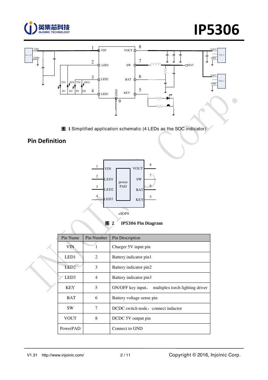
图 1 Simplified application schematic (4 LEDs as the SOC indicator)
Pin Definition
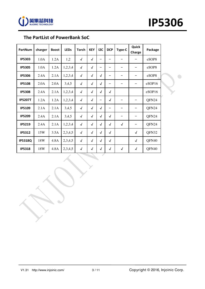
图 2 IP5306 Pin Diagram
Pin Name
Pin Number Pin Description
VIN
LED1
LED2
LED3
KEY
BAT
SW
VOUT
PowerPAD
1
2
3
4
5
6
7
8
Charger 5V input pin
Battery indicator pin1
Battery indicator pin2
Battery indicator pin3
ON/OFF key input, multiplex torch lighting driver
Battery voltage sense pin
DCDC switch node,connect inductor
DCDC 5V output pin
Connect to GND
V1.31 http://www.injoinic.com/ 2 / 11 Copyright © 2016, Injoinic Corp.
Micro-BVINGNDTYPE-AVOUTGNDVINVOUTLED1LED2LED3KEYBATSW123487659GNDTYPE-AVOUTGNDBAT25%50%75%100%D1D2D3D4VINLED2VOUTSWBATKEYLED112345678eSOP8powerPADLED3�
IP5306
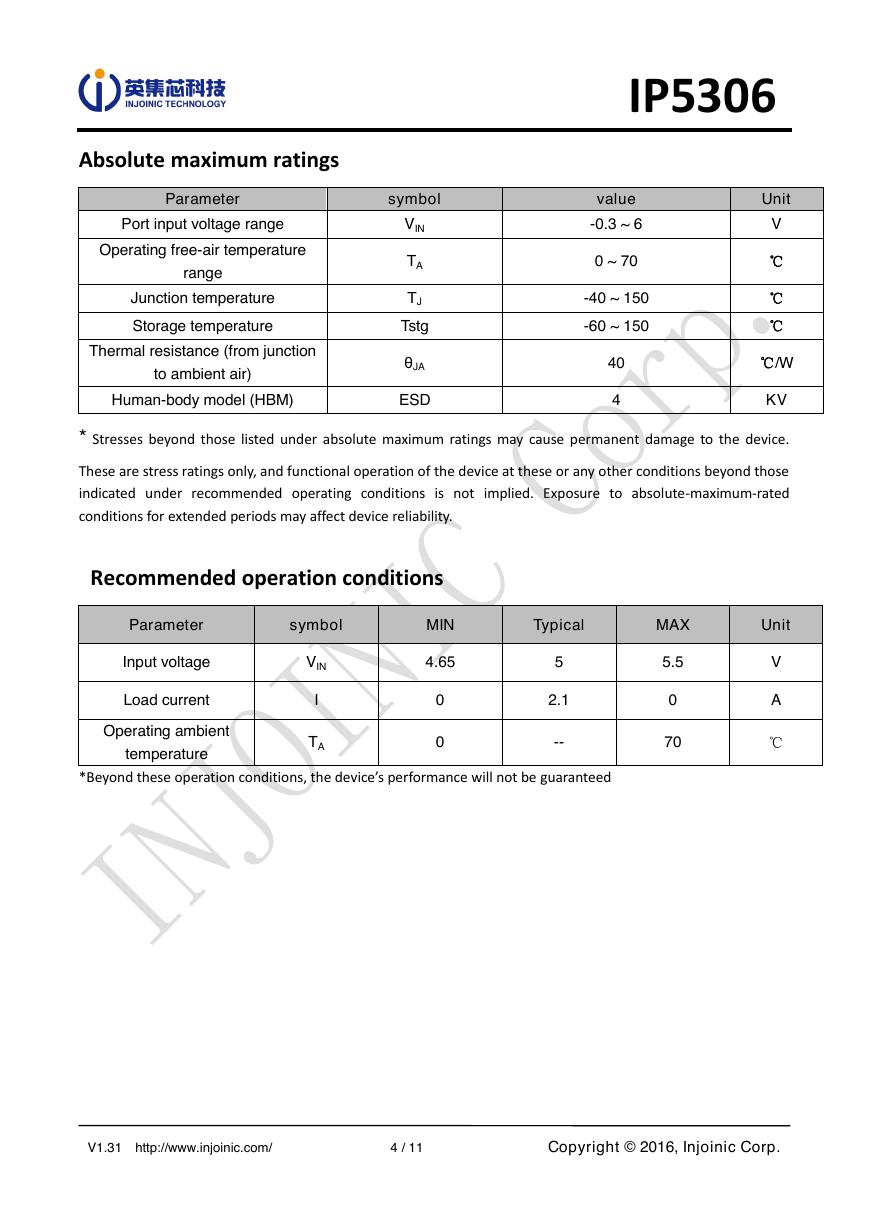
The PartList of PowerBank SoC
PartNum charger Boost
LEDs
Torch KEY
I2C DCP Type-C
IP5303
1.0A
1.2A
1,2
√ √
-
IP5305
1.0A
1.2A 1,2,3,4 √ √
-
IP5306
2.4A
2.1A 1,2,3,4 √ √ √
IP5108
2.0A
2.0A
3,4,5 √ √ √
-
-
-
-
IP5308
2.4A
2.1A 1,2,3,4 √ √ √ √
IP5207T
1.2A
1.2A 1,2,3,4 √ √
- √
IP5109
2.1A
2.1A
3,4,5 √ √ √
-
IP5209
2.4A
2.1A
3,4,5 √ √ √ √
-
-
-
-
-
-
-
IP5219
2.4A
2.1A 1,2,3,4 √ √ √ √ √
IP5312
15W
3.5A 2,3,4,5 √ √ √ √
IP5318Q
18W
IP5318
18W
4.8A 2,3,4,5 √ √ √ √
4.8A 2,3,4,5 √ √ √ √ √
Quick
Charge
Package
-
-
-
-
-
-
-
-
√
√
√
eSOP8
eSOP8
eSOP8
eSOP16
eSOP16
QFN24
QFN24
QFN24
QFN24
QFN32
QFN40
QFN40
V1.31 http://www.injoinic.com/ 3 / 11 Copyright © 2016, Injoinic Corp.
�
IP5306
Absolute maximum ratings
Parameter
symbol
Port input voltage range
Operating free-air temperature
range
Junction temperature
Storage temperature
Thermal resistance (from junction
to ambient air)
Human-body model (HBM)
VIN
TA
TJ
Tstg
θJA
ESD
value
-0.3 ~ 6
0 ~ 70
-40 ~ 150
-60 ~ 150
40
4
Unit
V
℃
℃
℃
℃/W
KV
* Stresses beyond those listed under absolute maximum ratings may cause permanent damage to the device.
These are stress ratings only, and functional operation of the device at these or any other conditions beyond those
indicated under recommended operating conditions is not implied. Exposure to absolute-maximum-rated
conditions for extended periods may affect device reliability.
Recommended operation conditions
Parameter
symbol
Input voltage
Load current
Operating ambient
temperature
VIN
I
TA
MIN
4.65
0
0
Typical
MAX
Unit
5
2.1
--
5.5
0
70
V
A
℃
*Beyond these operation conditions, the device’s performance will not be guaranteed
V1.31 http://www.injoinic.com/ 4 / 11 Copyright © 2016, Injoinic Corp.
�
IP5306
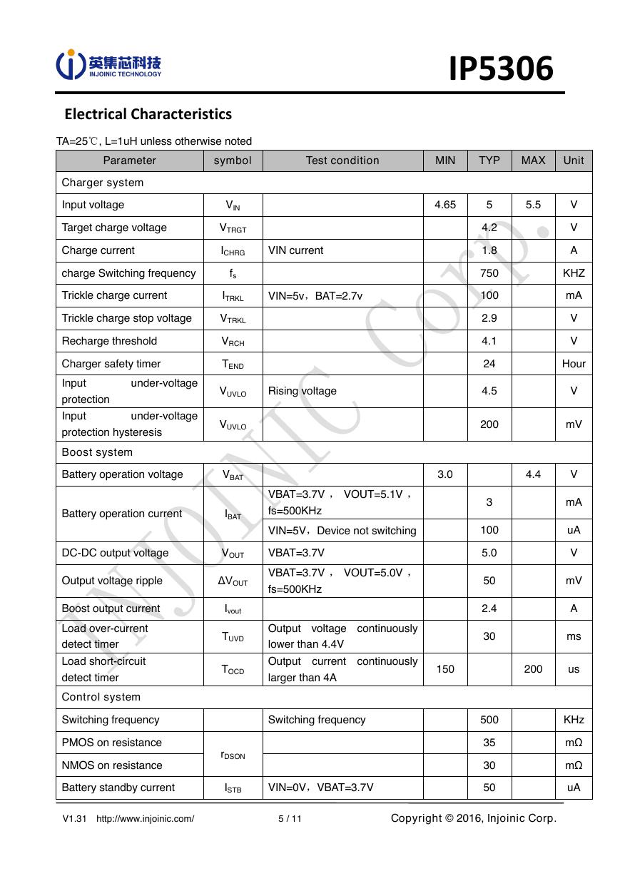
Electrical Characteristics
TA=25℃, L=1uH unless otherwise noted
Parameter
symbol
Test condition
MIN
TYP MAX Unit
4.65
5
5.5
4.2
1.8
750
100
2.9
4.1
24
4.5
200
3.0
3
100
5.0
50
2.4
30
V
V
A
KHZ
mA
V
V
Hour
V
mV
4.4
V
mA
uA
V
mV
A
ms
Charger system
Input voltage
Target charge voltage
VIN
VTRGT
Charge current
ICHRG
VIN current
charge Switching frequency
fs
Trickle charge current
ITRKL
VIN=5v,BAT=2.7v
Trickle charge stop voltage
VTRKL
Recharge threshold
Charger safety timer
VRCH
TEND
Input
under-voltage
protection
VUVLO
Rising voltage
Input
under-voltage
protection hysteresis
VUVLO
Boost system
Battery operation voltage
VBAT
Battery operation current
IBAT
VBAT=3.7V , VOUT=5.1V ,
fs=500KHz
VIN=5V,Device not switching
DC-DC output voltage
VOUT
VBAT=3.7V
Output voltage ripple
ΔVOUT
VBAT=3.7V , VOUT=5.0V ,
fs=500KHz
Boost output current
Ivout
Load over-current
detect timer
Load short-circuit
detect timer
Control system
TUVD
TOCD
Output voltage continuously
lower than 4.4V
Output current continuously
larger than 4A
Switching frequency
Switching frequency
PMOS on resistance
NMOS on resistance
rDSON
Battery standby current
ISTB
VIN=0V,VBAT=3.7V
150
200
us
500
35
30
50
KHz
mΩ
mΩ
uA
V1.31 http://www.injoinic.com/ 5 / 11 Copyright © 2016, Injoinic Corp.
�
IP5306
LED lighting current
Ilight
LED indicator current
IL1
IL2
IL3
Load removal detect timer
TloadD
Load
current
continuously
lower than 45mA
Push-button wake-up timer
TOnDebounc
e
Push-button light-on timer
TKeylight
Thermal shutdown
TOTP
Rising temperature
Thermal
hysteresis
shutdown
ΔTOTP
25
4
32
50
2
125
40
mA
mA
s
ms
s
℃
℃
V1.31 http://www.injoinic.com/ 6 / 11 Copyright © 2016, Injoinic Corp.
�
IP5306
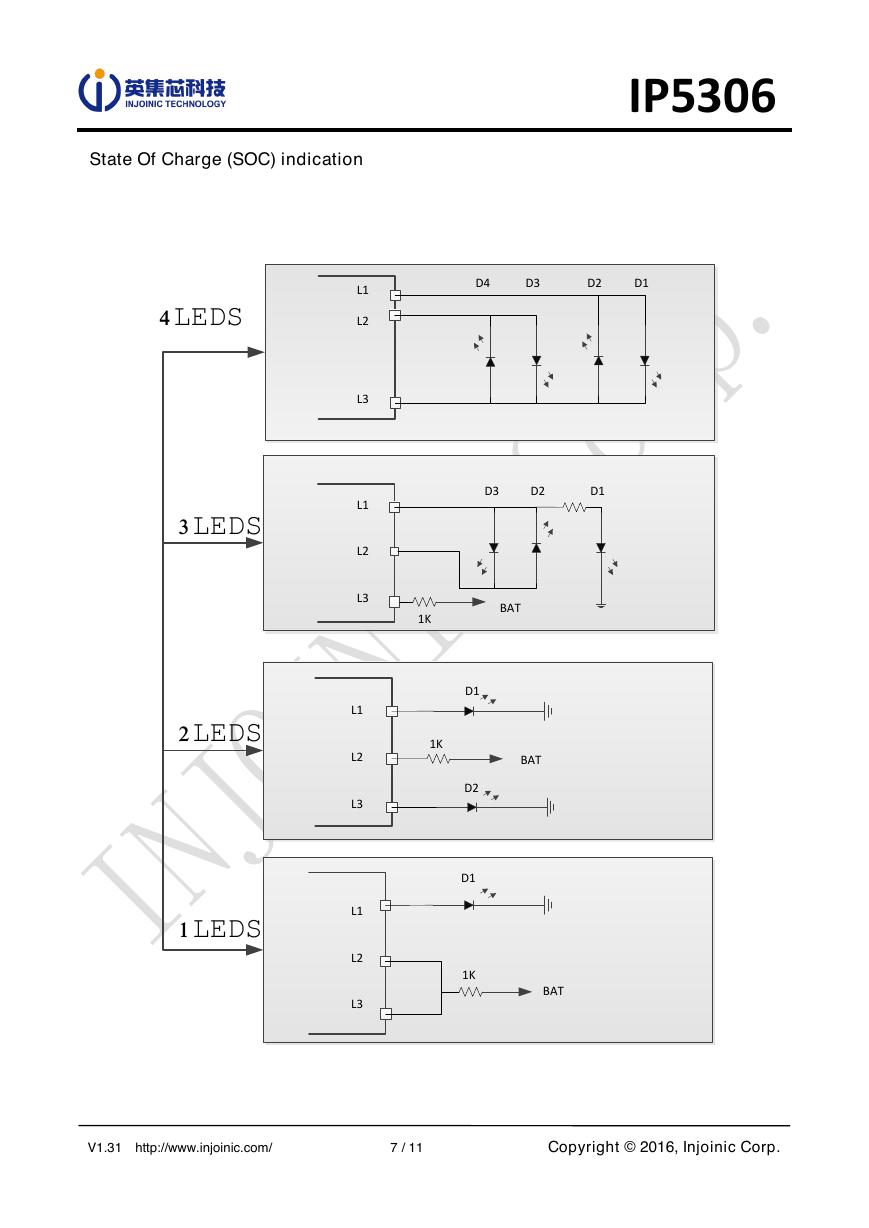
State Of Charge (SOC) indication
V1.31 http://www.injoinic.com/ 7 / 11 Copyright © 2016, Injoinic Corp.
4LEDS3LEDS2LEDSD3BAT1LEDSBAT D1 L1L2L3L1L2L3L1L2L3BATL1L2L3D2 D1 D2D1D4 D3 D2 D11K1K1K�
IP5306
4 LEDs mode
Discharging mode, 4 LEDs as the indicator
SOC(%)
SOC≥75%
50%≤SOC<75%
25%≤SOC<50%
3%≤SOC<25%
L1
ON
ON
ON
ON
0%<SOC<3%
1.5Hz blink
SOC=0%
OFF
L2
ON
ON
ON
OFF
OFF
OFF
Charging mode 4 LEDs as the indicator
SOC(%)
Full
75%≤SOC
50%≤SOC<75%
25%≤SOC<50%
L1
ON
ON
ON
ON
L2
ON
ON
ON
0.5Hz blink
SOC<25%
0.5Hz blink
OFF
L3
ON
ON
OFF
OFF
OFF
OFF
L3
ON
ON
L4
ON
OFF
OFF
OFF
OFF
OFF
L4
ON
0.5Hz blink
0.5Hz blink
OFF
OFF
OFF
OFF
OFF
3 LEDs mode
The displays of 3 LEDs is similar to that of 4 LEDs. The corresponding SOC of each LED is
presented in the following table.
3 LEDs
4 LEDs
D1
33%
25%
D2
66%
50%
D3
100%
75%
D4
NA
100%
D5
NA
NA
LED2
OFF
OFF
ON
Blink
2 LEDs Mode
state
Charging
In charging
End of Charge
Boost
In discharging
Low Battery
1 LED Mode
状态
Charging
In charging
End of Charge
Boost
In discharging
LED1
Blink
ON
OFF
OFF
LED1
Blink
ON
ON
Low Battery
Blink
V1.31 http://www.injoinic.com/ 8 / 11 Copyright © 2016, Injoinic Corp.
�



 V2版本原理图(Capacitive-Fingerprint-Reader-Schematic_V2).pdf
 摄像头工作原理.doc
 VL53L0X简要说明(En.FLVL53L00216).pdf
 原理图(DVK720-Schematic).pdf
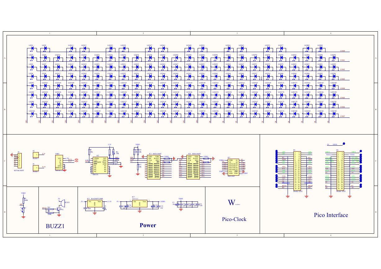 原理图(Pico-Clock-Green-Schdoc).pdf
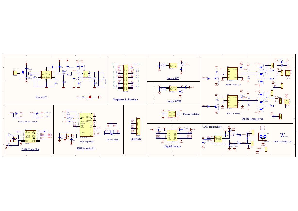 原理图(RS485-CAN-HAT-B-schematic).pdf
 File:SIM7500_SIM7600_SIM7800 Series_SSL_Application Note_V2.00.pdf
 ADS1263(Ads1262).pdf
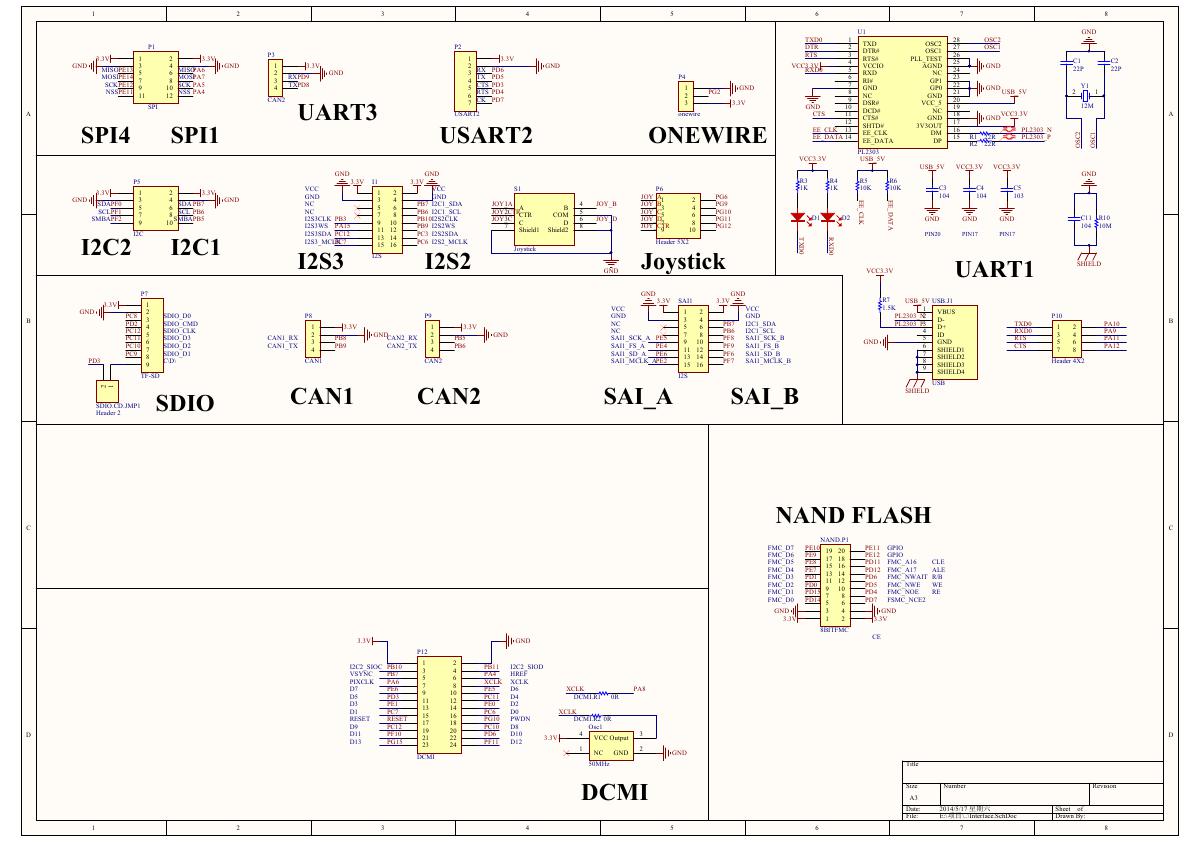 原理图(Open429Z-D-Schematic).pdf
 用户手册(Capacitive_Fingerprint_Reader_User_Manual_CN).pdf
 CY7C68013A(英文版)(CY7C68013A).pdf
 TechnicalReference_Dem.pdf