Preliminary Specification
PRODUCT NUMBER: 0.96inch RGB OLED
0.96inch RGB OLED1 / 41�
REVISION RECORD
REV. REVISION DESCRIPTION
X01
X02
X03
X04
REV. DATE REMARK
2017. 09. 04
INITIAL RELEASE
Add dot size specification
2017. 09. 28 Page 5 & 19
Modify outgoing inspection provision 2017. 10. 23 Page 23~27
Add panel electrical specifications
Add lifetime specification
2017. 11. 03 Page 7, 8 & 9
■
■
■
■
■
0.96inch RGB OLED2 / 41�
CONTENTS
ITEM
1. SCOPE
2. WARRANTY
3. FEATURES
4. MECHANICAL DATA
5. MAXIMUM RATINGS
6. ELECTRICAL CHARACTERISTICS
6.1 D.C ELECTRICAL CHARACTERISTICS
6.2 ELECTRO-OPTICAL CHARACTERISTICS
7. LIFETIME SPECIFICATION
8. INTERFACE
8.1 FUNCTION BLOCK DIAGRAM
8.2 PANEL LAYOUT DIAGRAM
8.3 PIN ASSIGNMENTS
8.4 GRAPHIC DISPLAY DATA RAM ADDRESS MAP
8.5 INTERFACE TIMING CHART
9. POWER ON / OFF SEQUENCE & APPLICATION CIRCUIT
9.1 POWER ON / OFF SEQUENCE
9.2 APPLICATION CIRCUIT
9.3 COMMAND TABLE
10. RELIABILITY TEST CONDITIONS
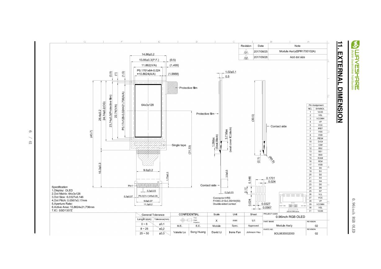
11. EXTERNAL DIMENSION
12. PACKING SPECIFICATION
13. OUTGOING INSPECTION PROVISION
14. APPENDIXES
PAGE
4
4
4
5
6
6
9
10
15
18
19
20
21
28
0.96inch RGB OLED3 / 41�
1. SCOPE
The purpose of this specification is to define the general provisions and quality
requirements that apply to the supply of display cells manufactured by Topwin
display. This document, together with the Module Assembly Drawing, is the
highest-level specification for this product. It describes the product, identifies
supporting documents and contains specifications.
2. WARRANTY
3. FEATURES
- Small molecular organic light emitting diode.
- Color : Full
- Panel resolution : 64x3x128
- Driver IC : SSD1357Z
- Excellent Quick response time : 10µs
- Extremely thin thickness for best mechanism design : 1.02 mm
- High contrast : 2000:1
- Wide viewing angle : 160°
- Interface: 8080-series parallel Interface and Serial Peripheral Interface
- Wide range of operating temperature : -40 to 70°C
0.96inch RGB OLED4 / 41�
4. MECHANICAL DATA
NO
ITEM
SPECIFICATION
UNIT
1 Dot Matrix
2 Dot Size
3 Dot Pitch
4 Active Area
5 Panel Size
6* Panel Thickness
7 Module Size
8 Diagonal A/A size
9 Module Weight
64 x 3 x 128
0.0327 (W) x 0.146 (H)
0.0567 (W) x 0.17 (H)
10.8624 (W) x 21.736 (H)
dot
mm2
mm2
mm2
mm2
mm
14.86 (W) x 43.7 (H) x 1.02 (T) mm3
inch
14.86 (W) x 28.4 (H)
1.02 ± 0.1
0.96
TBD
gram
* Panel thickness includes substrate glass, cover glass and UV glue
thickness.
0.96inch RGB OLED5 / 41�
1
1
.
E
X
T
E
R
N
A
L
D
M
E
N
S
O
N
I
I
0.96inch RGB OLED
0.96inch RGB OLED6 / 41�
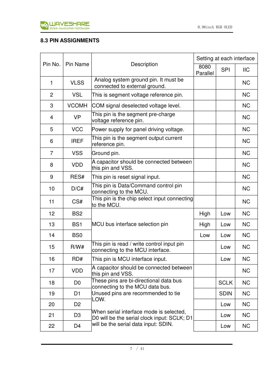
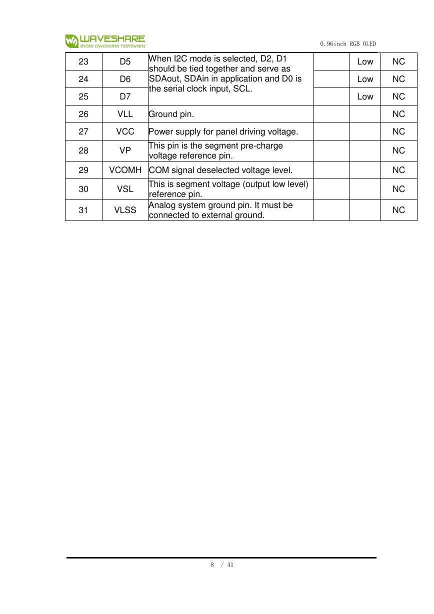
8.3 PIN ASSIGNMENTS
Pin No. Pin Name
Description
Setting at each interface
8080
Parallel
SPI
IIC
1
2
3
4
5
6
7
8
9
10
11
12
13
14
15
16
17
18
19
20
21
22
VLSS
VSL
Analog system ground pin. It must be
connected to external ground.
This is segment voltage reference pin.
VCOMH COM signal deselected voltage level.
VP
This pin is the segment pre-charge
voltage reference pin.
VCC Power supply for panel driving voltage.
IREF
This pin is the segment output current
reference pin.
VSS Ground pin.
VDD
A capacitor should be connected between
this pin and VSS.
RES# This pin is reset signal input.
This pin is Data/Command control pin
connecting to the MCU.
This pin is the chip select input connecting
to the MCU.
MCU bus interface selection pin
D/C#
CS#
BS2
BS1
BS0
High
Low
High
Low
Low
Low
NC
NC
NC
NC
NC
NC
NC
NC
NC
NC
NC
NC
NC
NC
R/W#
This pin is read / write control input pin
connecting to the MCU interface.
RD#
This pin is MCU interface input.
VDD
D0
D1
D2
D3
D4
A capacitor should be connected between
this pin and VSS.
These pins are bi-directional data bus
connecting to the MCU data bus.
Unused pins are recommended to tie
LOW.
When serial interface mode is selected,
D0 will be the serial clock input: SCLK; D1
will be the serial data input: SDIN.
Low
NC
Low
NC
NC
SCLK
NC
SDIN
NC
Low
Low
Low
NC
NC
NC
0.96inch RGB OLED7 / 41�
23
24
25
26
27
28
29
30
31
When I2C mode is selected, D2, D1
should be tied together and serve as
SDAout, SDAin in application and D0 is
the serial clock input, SCL.
D5
D6
D7
VLL Ground pin.
VCC Power supply for panel driving voltage.
VP
This pin is the segment pre-charge
voltage reference pin.
VCOMH COM signal deselected voltage level.
VSL
VLSS
This is segment voltage (output low level)
reference pin.
Analog system ground pin. It must be
connected to external ground.
Low
Low
Low
NC
NC
NC
NC
NC
NC
NC
NC
NC
0.96inch RGB OLED8 / 41�




 V2版本原理图(Capacitive-Fingerprint-Reader-Schematic_V2).pdf
 摄像头工作原理.doc
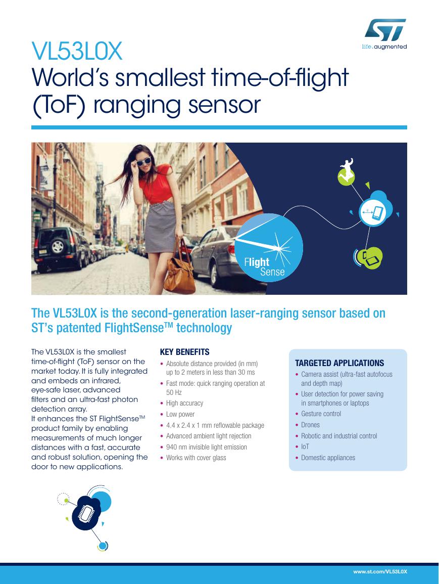 VL53L0X简要说明(En.FLVL53L00216).pdf
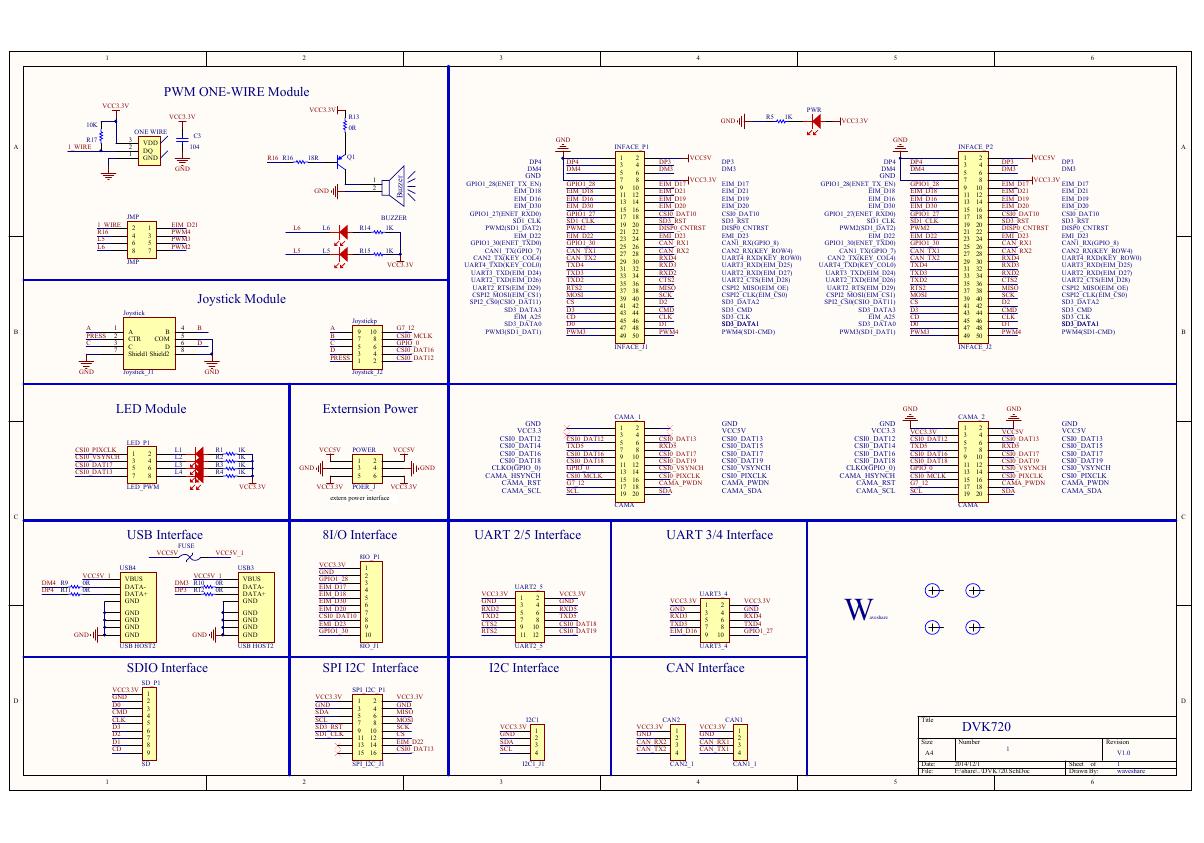 原理图(DVK720-Schematic).pdf
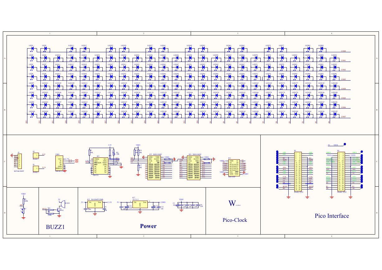 原理图(Pico-Clock-Green-Schdoc).pdf
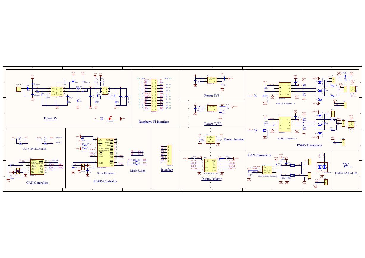 原理图(RS485-CAN-HAT-B-schematic).pdf
 File:SIM7500_SIM7600_SIM7800 Series_SSL_Application Note_V2.00.pdf
 ADS1263(Ads1262).pdf
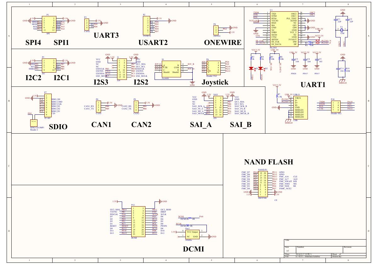 原理图(Open429Z-D-Schematic).pdf
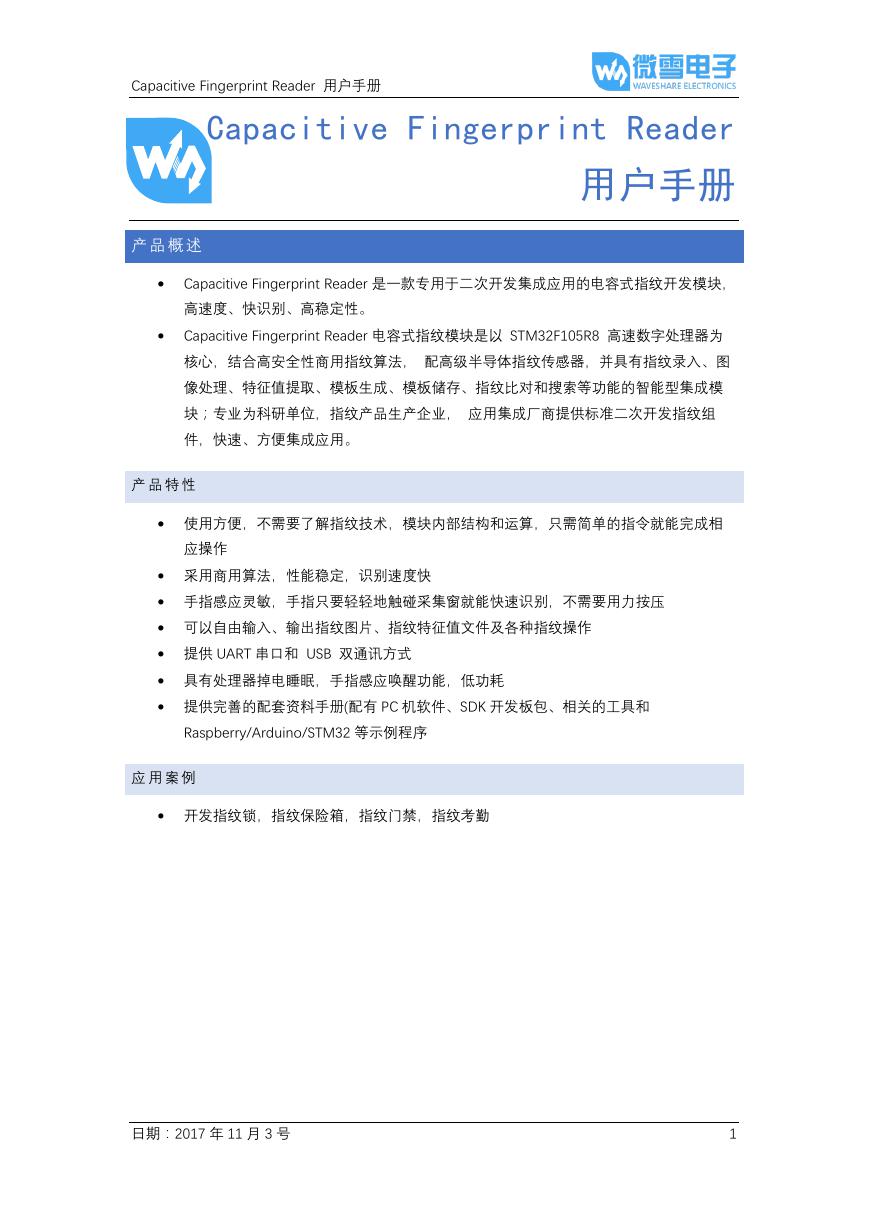 用户手册(Capacitive_Fingerprint_Reader_User_Manual_CN).pdf
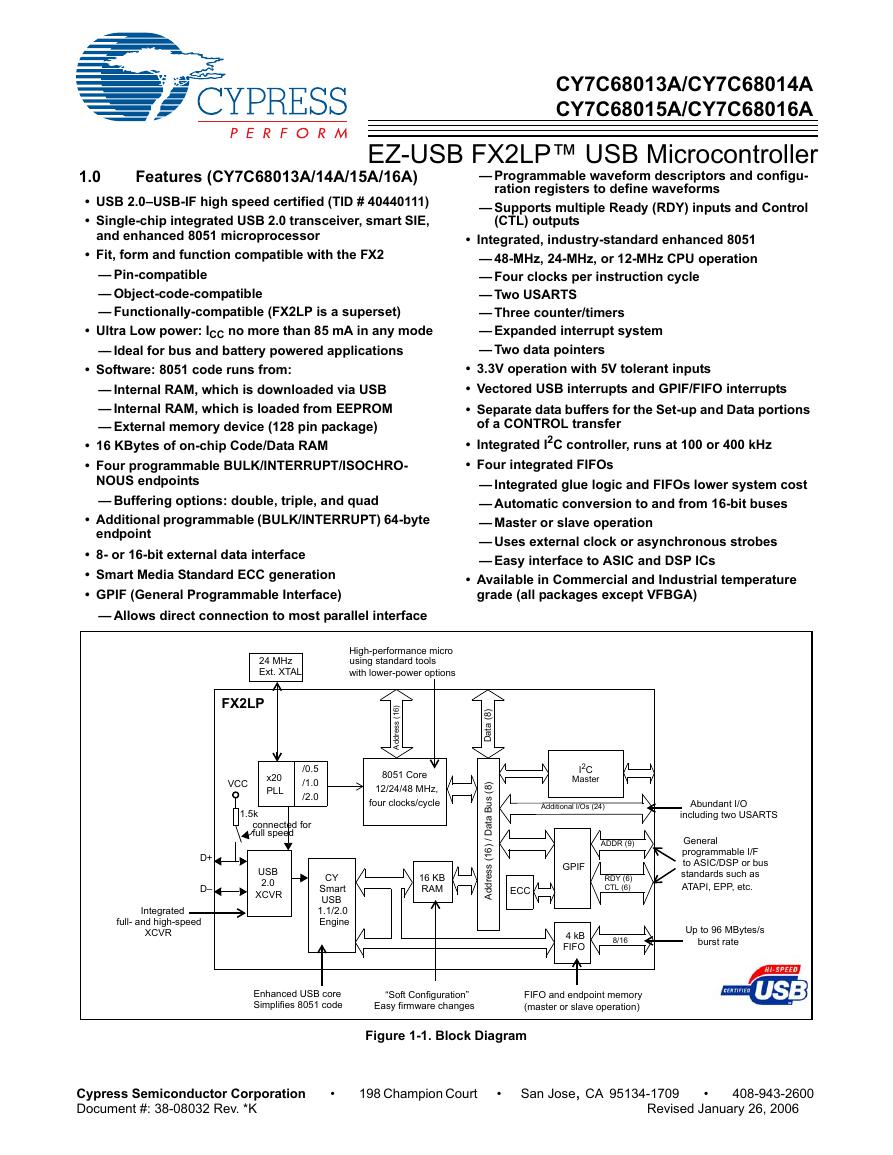 CY7C68013A(英文版)(CY7C68013A).pdf
 TechnicalReference_Dem.pdf