Version: 0.2
Technical Specification
MODEL NO:
5.65inch e-Paper (F)
The content of this information is subject to be changed without notice.
Please contact Waveshare for further information
5.65inch e-PaperPAGE1�
Rev.
Issued Date
Revised Contents
Revision History
0.1
0.1
0.2
2019.10.16
Tentative
2019.10.30
Preliminary
2019.11.19
Update Page 17: Remove R65H (DAM) SPI Flash control
5.65inch e-PaperPAGE2�
TECHNICAL SPECIFICATION
CONTENTS
ITEM
Cover
Revision History
Contents
General Description
Features
Mechanical Specifications
Mechanical Drawing of EPD module
Input/Output Terminals
Command Table
Electrical Characteristics
Optical Characteristics
Handling, Safety and Environment Requirements
and Remark
Reliability test
Block Diagram
Packing
NO.
-
-
-
1
2
3
4
5
6
7
8
9
10
11
12
PAGE
1
2
3
4
4
4
5
6
8
19
26
27
29
30
31
5.65inch e-PaperPAGE3�
1. General Description
This is a reflective electrophoretic E Ink® technology display module on an active matrixTFT
substrate. The diagonal length of the active area is 5.65” and contains 600 x 448 pixels. The panelis
capable of displaying 7-colors of black, white, red, yellow, blue, green, and orange images
depending on the associated lookup table used. The circuitry on the panel includes an integrated gate
and source driver, timing controller, oscillator, DC-DC boost circuit, and memory to store the frame
buffer and lookup tables, and additional circuitry to control VCOM and BORDER settings.
2.
Features
7-color ACeP display
High contrast TFT electrophoretic
600 x 448 display
High reflectance
Ultra wide viewing angle
Ultra low power consumption
Pure reflective mode
Bi-stable
Low current sleep mode
On chip display RAM
Serial Peripheral Interface
External SPI flash/eeprom for waveform
On-chip oscillator
On-chip booster and regulator control for generating Vcom, Gate and Source driving voltage
I2C Signal Master Interface to read external temperature sensor
Operational temperature range (15 ~ 35℃)
3.
Mechanical Specifications
Parameter
Screen Size
Specifications
5.65”
Display Resolution
600 (H) × 448 (V)
Active Area
Pixel Pitch
114.9 (H) × 85.8 (V)
191.5 (H) × 191.5 (V)
Pixel Configuration
Square
Outline Dimension
125.4 (H) × 99.5 (V) × 0.91 (D)
Weight
TBD
Number of Colors
Black, White, Red, Yellow, Blue, Green and Orange
Display operating mode
Reflective mode
Unit
Inch
Remark
-
Pixel
132 dpi
mm
um
mm
g
-
-
-
Without
protective film
-
5.65inch e-PaperPAGE4�
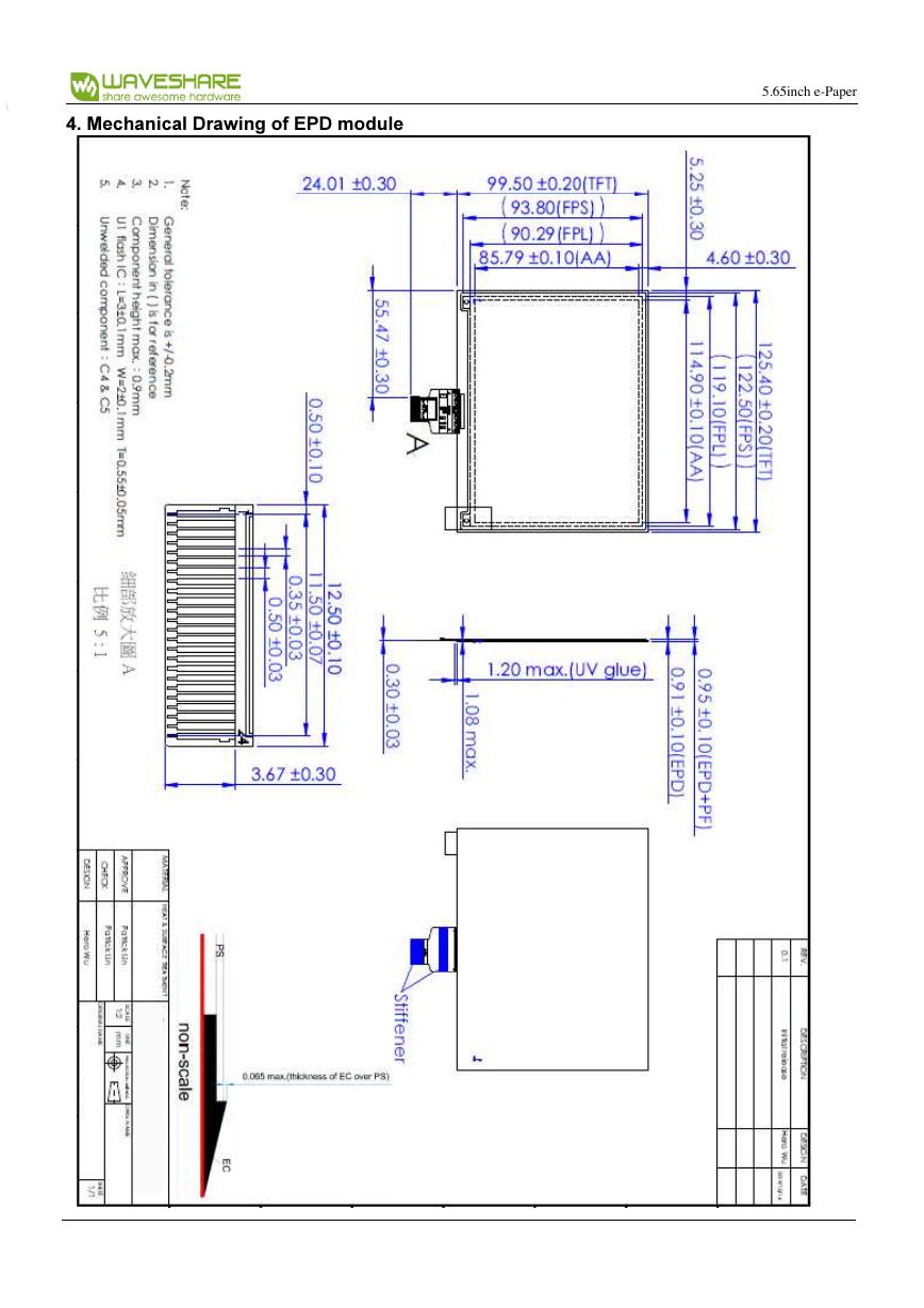
4. Mechanical Drawing of EPD module
5.65inch e-Paper�
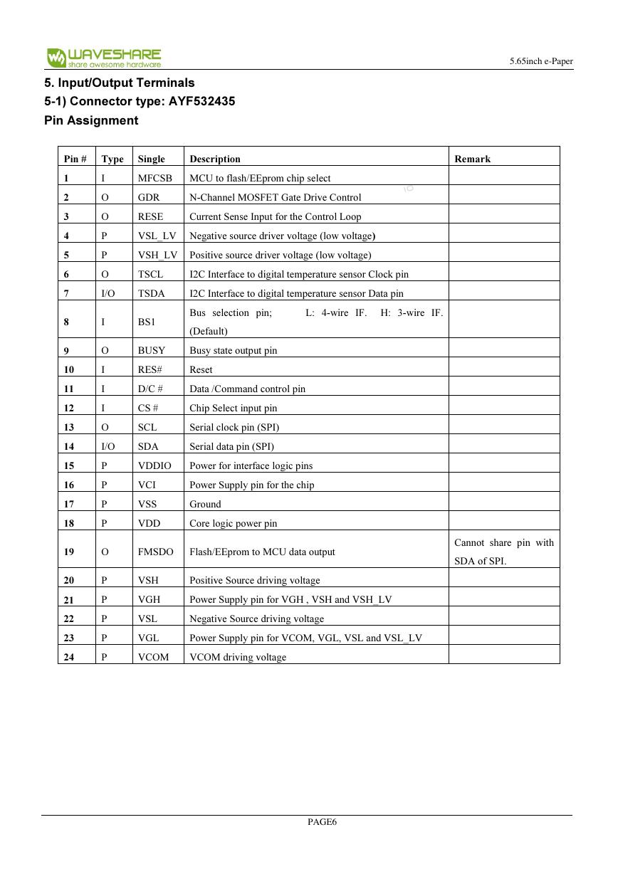
5. Input/Output Terminals
5-1) Connector type: AYF532435
Pin Assignment
Pin # Type
Single
Description
Remark
1
2
3
4
5
6
7
8
9
10
11
12
13
14
15
16
17
18
I
O
O
P
P
O
MFCSB MCU to flash/EEprom chip select
GDR
N-Channel MOSFET Gate Drive Control
RESE
Current Sense Input for the Control Loop
VSL_LV Negative source driver voltage (low voltage)
VSH_LV Positive source driver voltage (low voltage)
TSCL
I2C Interface to digital temperature sensor Clock pin
I/O
TSDA
I2C Interface to digital temperature sensor Data pin
I
O
I
I
I
O
BS1
Bus selection pin;
L: 4-wire IF. H: 3-wire IF.
(Default)
BUSY
Busy state output pin
RES#
Reset
D/C #
Data /Command control pin
CS #
SCL
Chip Select input pin
Serial clock pin (SPI)
I/O
SDA
Serial data pin (SPI)
P
P
P
P
VDDIO
Power for interface logic pins
VCI
VSS
Power Supply pin for the chip
Ground
VDD
Core logic power pin
19
O
FMSDO
Flash/EEprom to MCU data output
20
21
22
23
24
P
P
P
P
P
VSH
Positive Source driving voltage
VGH
Power Supply pin for VGH , VSH and VSH_LV
VSL
VGL
Negative Source driving voltage
Power Supply pin for VCOM, VGL, VSL and VSL_LV
VCOM
VCOM driving voltage
Cannot share pin with
SDA of SPI.
5.65inch e-PaperPAGE6�
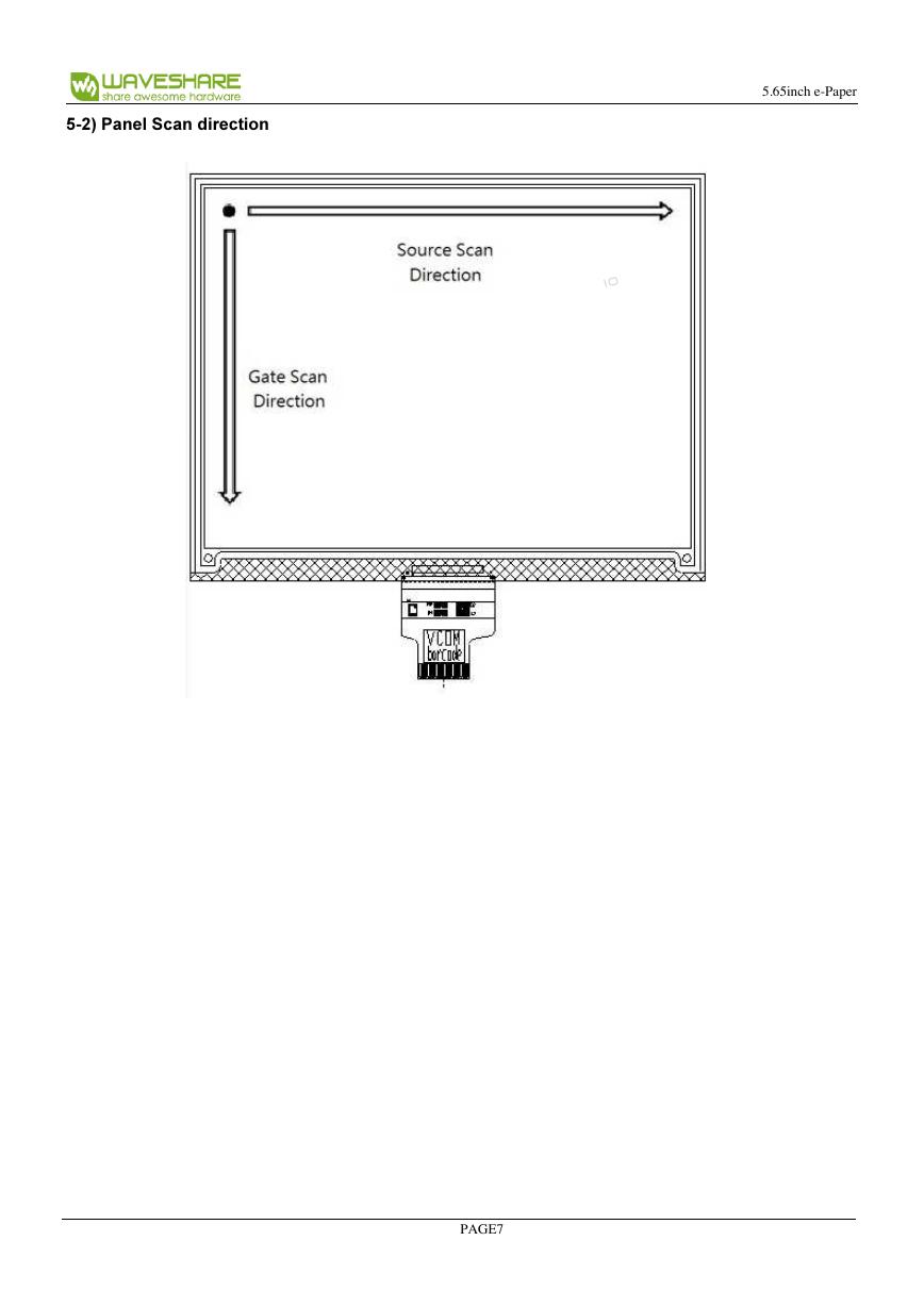
5-2) Panel Scan direction
5.65inch e-PaperPAGE7�
6. Command Table
6-1) Register Definition
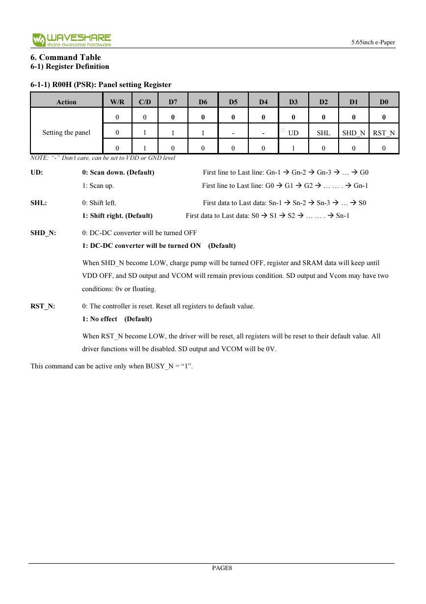
6-1-1) R00H (PSR): Panel setting Register
Action
W/R
C/D
D7
D6
D5
D4
D3
D2
D1
D0
Setting the panel
0
0
0
0
1
1
0
1
0
0
1
0
0
-
0
0
-
0
0
0
0
0
UD
SHL
SHD_N RST_N
1
0
0
0
NOTE: “-” Don’t care, can be set to VDD or GND level
UD:
0: Scan down. (Default)
First line to Last line: Gn-1 � Gn-2 � Gn-3 � … � G0
1: Scan up.
First line to Last line: G0 � G1 � G2 � … … . � Gn-1
SHL:
0: Shift left.
First data to Last data: Sn-1 � Sn-2 � Sn-3 � … � S0
1: Shift right. (Default)
First data to Last data: S0 � S1 � S2 � … … . � Sn-1
SHD_N:
0: DC-DC converter will be turned OFF
1: DC-DC converter will be turned ON (Default)
When SHD_N become LOW, charge pump will be turned OFF, register and SRAM data will keep until
VDD OFF, and SD output and VCOM will remain previous condition. SD output and Vcom may have two
conditions: 0v or floating.
RST_N:
0: The controller is reset. Reset all registers to default value.
1: No effect (Default)
When RST_N become LOW, the driver will be reset, all registers will be reset to their default value. All
driver functions will be disabled. SD output and VCOM will be 0V.
This command can be active only when BUSY_N = “1”.
5.65inch e-PaperPAGE8�



 V2版本原理图(Capacitive-Fingerprint-Reader-Schematic_V2).pdf
 摄像头工作原理.doc
 VL53L0X简要说明(En.FLVL53L00216).pdf
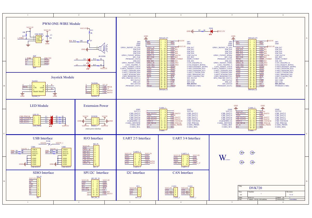 原理图(DVK720-Schematic).pdf
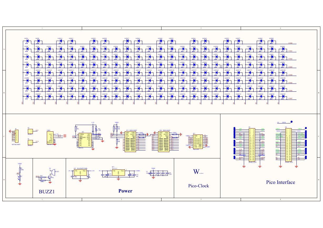 原理图(Pico-Clock-Green-Schdoc).pdf
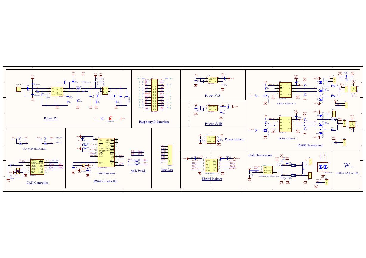 原理图(RS485-CAN-HAT-B-schematic).pdf
 File:SIM7500_SIM7600_SIM7800 Series_SSL_Application Note_V2.00.pdf
 ADS1263(Ads1262).pdf
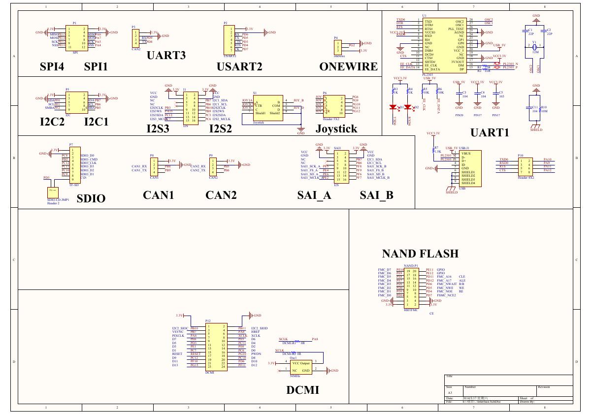 原理图(Open429Z-D-Schematic).pdf
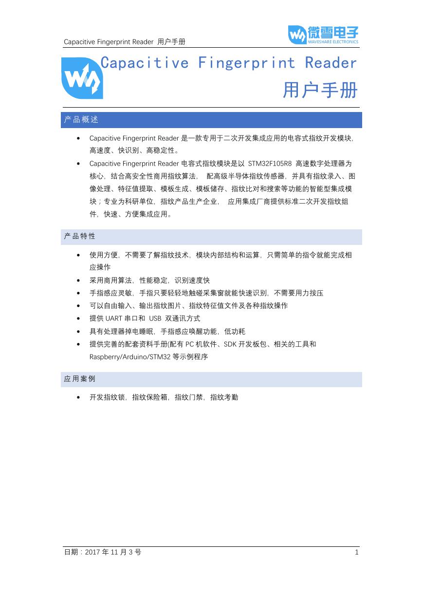 用户手册(Capacitive_Fingerprint_Reader_User_Manual_CN).pdf
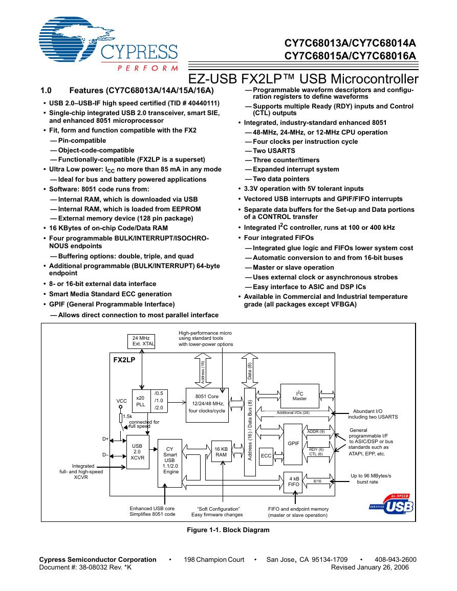 CY7C68013A(英文版)(CY7C68013A).pdf
 TechnicalReference_Dem.pdf