�
Hardware design with RP2040
Colophon
Copyright © 2020-2022 Raspberry Pi Ltd (formerly Raspberry Pi (Trading) Ltd.)
The documentation of the RP2040 microcontroller is licensed under a Creative Commons Attribution-NoDerivatives 4.0
International (CC BY-ND).
build-date: 2022-06-29
build-version: 6a06c22-dirty
About the SDK
Throughout the text "the SDK" refers to our Raspberry Pi Pico SDK. More details about the SDK can be
found in the Raspberry Pi Pico C/C++ SDK book. Source code included in the documentation is
Copyright © 2020-2022 Raspberry Pi Ltd (formerly Raspberry Pi (Trading) Ltd.) and licensed under the 3-
Clause BSD license.
Legal disclaimer notice
TECHNICAL AND RELIABILITY DATA FOR RASPBERRY PI PRODUCTS (INCLUDING DATASHEETS) AS MODIFIED FROM
TIME TO TIME (“RESOURCES”) ARE PROVIDED BY RASPBERRY PI LTD (“RPL”) "AS IS" AND ANY EXPRESS OR IMPLIED
WARRANTIES, INCLUDING, BUT NOT LIMITED TO, THE IMPLIED WARRANTIES OF MERCHANTABILITY AND FITNESS
FOR A PARTICULAR PURPOSE ARE DISCLAIMED. TO THE MAXIMUM EXTENT PERMITTED BY APPLICABLE LAW IN NO
EVENT SHALL RPL BE LIABLE FOR ANY DIRECT, INDIRECT, INCIDENTAL, SPECIAL, EXEMPLARY, OR CONSEQUENTIAL
DAMAGES (INCLUDING, BUT NOT LIMITED TO, PROCUREMENT OF SUBSTITUTE GOODS OR SERVICES; LOSS OF USE,
DATA, OR PROFITS; OR BUSINESS INTERRUPTION) HOWEVER CAUSED AND ON ANY THEORY OF LIABILITY, WHETHER
IN CONTRACT, STRICT LIABILITY, OR TORT (INCLUDING NEGLIGENCE OR OTHERWISE) ARISING IN ANY WAY OUT OF
THE USE OF THE RESOURCES, EVEN IF ADVISED OF THE POSSIBILITY OF SUCH DAMAGE.
RPL reserves the right to make any enhancements, improvements, corrections or any other modifications to the
RESOURCES or any products described in them at any time and without further notice.
The RESOURCES are intended for skilled users with suitable levels of design knowledge. Users are solely responsible for
their selection and use of the RESOURCES and any application of the products described in them. User agrees to
indemnify and hold RPL harmless against all liabilities, costs, damages or other losses arising out of their use of the
RESOURCES.
RPL grants users permission to use the RESOURCES solely in conjunction with the Raspberry Pi products. All other use
of the RESOURCES is prohibited. No licence is granted to any other RPL or other third party intellectual property right.
HIGH RISK ACTIVITIES. Raspberry Pi products are not designed, manufactured or intended for use in hazardous
environments requiring fail safe performance, such as in the operation of nuclear facilities, aircraft navigation or
communication systems, air traffic control, weapons systems or safety-critical applications (including life support
systems and other medical devices), in which the failure of the products could lead directly to death, personal injury or
severe physical or environmental damage (“High Risk Activities”). RPL specifically disclaims any express or implied
warranty of fitness for High Risk Activities and accepts no liability for use or inclusions of Raspberry Pi products in High
Risk Activities.
Raspberry Pi products are provided subject to RPL’s Standard Terms. RPL’s provision of the RESOURCES does not
expand or otherwise modify RPL’s Standard Terms including but not limited to the disclaimers and warranties
expressed in them.
Legal disclaimer notice
1
Hardware design with RP2040
Table of contents
Colophon . . . . . . . . . . . . . . . . . . . . . . . . . . . . . . . . . . . . . . . . . . . . . . . . . . . . . . . . . . . . . . . . . . . . . . . . . . . . . . . . . . . . . . . . . . . . . . 1
Legal disclaimer notice . . . . . . . . . . . . . . . . . . . . . . . . . . . . . . . . . . . . . . . . . . . . . . . . . . . . . . . . . . . . . . . . . . . . . . . . . . . . . . . 1
1. About the RP2040 . . . . . . . . . . . . . . . . . . . . . . . . . . . . . . . . . . . . . . . . . . . . . . . . . . . . . . . . . . . . . . . . . . . . . . . . . . . . . . . . . . . . 3
2. Minimal design example . . . . . . . . . . . . . . . . . . . . . . . . . . . . . . . . . . . . . . . . . . . . . . . . . . . . . . . . . . . . . . . . . . . . . . . . . . . . . . . 5
2.1. Power . . . . . . . . . . . . . . . . . . . . . . . . . . . . . . . . . . . . . . . . . . . . . . . . . . . . . . . . . . . . . . . . . . . . . . . . . . . . . . . . . . . . . . . . . . 6
2.1.1. Input supply . . . . . . . . . . . . . . . . . . . . . . . . . . . . . . . . . . . . . . . . . . . . . . . . . . . . . . . . . . . . . . . . . . . . . . . . . . . . . . . . 6
2.1.2. Decoupling capacitors. . . . . . . . . . . . . . . . . . . . . . . . . . . . . . . . . . . . . . . . . . . . . . . . . . . . . . . . . . . . . . . . . . . . . . . . 7
2.1.3. Internal voltage regulator . . . . . . . . . . . . . . . . . . . . . . . . . . . . . . . . . . . . . . . . . . . . . . . . . . . . . . . . . . . . . . . . . . . . . 7
2.2. Flash storage . . . . . . . . . . . . . . . . . . . . . . . . . . . . . . . . . . . . . . . . . . . . . . . . . . . . . . . . . . . . . . . . . . . . . . . . . . . . . . . . . . . . 8
2.3. Crystal oscillator . . . . . . . . . . . . . . . . . . . . . . . . . . . . . . . . . . . . . . . . . . . . . . . . . . . . . . . . . . . . . . . . . . . . . . . . . . . . . . . . . 8
2.4. I/Os . . . . . . . . . . . . . . . . . . . . . . . . . . . . . . . . . . . . . . . . . . . . . . . . . . . . . . . . . . . . . . . . . . . . . . . . . . . . . . . . . . . . . . . . . . . . 9
2.4.1. USB . . . . . . . . . . . . . . . . . . . . . . . . . . . . . . . . . . . . . . . . . . . . . . . . . . . . . . . . . . . . . . . . . . . . . . . . . . . . . . . . . . . . . . . 9
2.4.2. I/O headers . . . . . . . . . . . . . . . . . . . . . . . . . . . . . . . . . . . . . . . . . . . . . . . . . . . . . . . . . . . . . . . . . . . . . . . . . . . . . . . . 10
2.5. Schematic . . . . . . . . . . . . . . . . . . . . . . . . . . . . . . . . . . . . . . . . . . . . . . . . . . . . . . . . . . . . . . . . . . . . . . . . . . . . . . . . . . . . . 11
2.6. Supported flash chips. . . . . . . . . . . . . . . . . . . . . . . . . . . . . . . . . . . . . . . . . . . . . . . . . . . . . . . . . . . . . . . . . . . . . . . . . . . . 12
2.7. Making a PCB . . . . . . . . . . . . . . . . . . . . . . . . . . . . . . . . . . . . . . . . . . . . . . . . . . . . . . . . . . . . . . . . . . . . . . . . . . . . . . . . . . 13
3. The VGA, SD card & audio demo boards for Raspberry Pi Pico and Raspberry Pi Pico W . . . . . . . . . . . . . . . . . . . . . . . . 14
3.1. Power . . . . . . . . . . . . . . . . . . . . . . . . . . . . . . . . . . . . . . . . . . . . . . . . . . . . . . . . . . . . . . . . . . . . . . . . . . . . . . . . . . . . . . . . . 15
3.1.1. Power input. . . . . . . . . . . . . . . . . . . . . . . . . . . . . . . . . . . . . . . . . . . . . . . . . . . . . . . . . . . . . . . . . . . . . . . . . . . . . . . . 15
3.1.2. Audio power supply . . . . . . . . . . . . . . . . . . . . . . . . . . . . . . . . . . . . . . . . . . . . . . . . . . . . . . . . . . . . . . . . . . . . . . . . . 18
3.2. VGA video . . . . . . . . . . . . . . . . . . . . . . . . . . . . . . . . . . . . . . . . . . . . . . . . . . . . . . . . . . . . . . . . . . . . . . . . . . . . . . . . . . . . . 18
3.2.1. Resistor DAC . . . . . . . . . . . . . . . . . . . . . . . . . . . . . . . . . . . . . . . . . . . . . . . . . . . . . . . . . . . . . . . . . . . . . . . . . . . . . . 19
3.2.2. User buttons . . . . . . . . . . . . . . . . . . . . . . . . . . . . . . . . . . . . . . . . . . . . . . . . . . . . . . . . . . . . . . . . . . . . . . . . . . . . . . . 20
3.3. SD card. . . . . . . . . . . . . . . . . . . . . . . . . . . . . . . . . . . . . . . . . . . . . . . . . . . . . . . . . . . . . . . . . . . . . . . . . . . . . . . . . . . . . . . . 21
3.3.1. UART . . . . . . . . . . . . . . . . . . . . . . . . . . . . . . . . . . . . . . . . . . . . . . . . . . . . . . . . . . . . . . . . . . . . . . . . . . . . . . . . . . . . . 21
3.3.2. Debug – SWD . . . . . . . . . . . . . . . . . . . . . . . . . . . . . . . . . . . . . . . . . . . . . . . . . . . . . . . . . . . . . . . . . . . . . . . . . . . . . . 22
3.4. Audio . . . . . . . . . . . . . . . . . . . . . . . . . . . . . . . . . . . . . . . . . . . . . . . . . . . . . . . . . . . . . . . . . . . . . . . . . . . . . . . . . . . . . . . . . 22
3.4.1. PWM audio . . . . . . . . . . . . . . . . . . . . . . . . . . . . . . . . . . . . . . . . . . . . . . . . . . . . . . . . . . . . . . . . . . . . . . . . . . . . . . . . 22
3.4.2. PCM/I2S audio . . . . . . . . . . . . . . . . . . . . . . . . . . . . . . . . . . . . . . . . . . . . . . . . . . . . . . . . . . . . . . . . . . . . . . . . . . . . . 23
3.5. Raspberry Pi Pico and Raspberry Pi Pico W . . . . . . . . . . . . . . . . . . . . . . . . . . . . . . . . . . . . . . . . . . . . . . . . . . . . . . . . . 23
3.6. Schematics . . . . . . . . . . . . . . . . . . . . . . . . . . . . . . . . . . . . . . . . . . . . . . . . . . . . . . . . . . . . . . . . . . . . . . . . . . . . . . . . . . . . 27
Appendix A: Using the rescue debug port . . . . . . . . . . . . . . . . . . . . . . . . . . . . . . . . . . . . . . . . . . . . . . . . . . . . . . . . . . . . . . . . . . 30
Overview . . . . . . . . . . . . . . . . . . . . . . . . . . . . . . . . . . . . . . . . . . . . . . . . . . . . . . . . . . . . . . . . . . . . . . . . . . . . . . . . . . . . . . . . . . 30
Activating the rescue DP from OpenOCD . . . . . . . . . . . . . . . . . . . . . . . . . . . . . . . . . . . . . . . . . . . . . . . . . . . . . . . . . . . . . . . 30
Appendix B: Documentation release history . . . . . . . . . . . . . . . . . . . . . . . . . . . . . . . . . . . . . . . . . . . . . . . . . . . . . . . . . . . . . . . . 32
Table of contents
2
�
Hardware design with RP2040
Chapter 1. About the RP2040
RP2040 is a low-cost, high-performance microcontroller device with flexible digital interfaces. Key features:
• Dual Cortex M0+ processors, up to 133MHz
• 264kB of embedded SRAM in 6 banks
• 30 multifunction GPIO
• 6 dedicated I/O for SPI flash (supporting XIP)
• Dedicated hardware for commonly used peripherals
• Programmable I/O for extended peripheral support
• 4 channel ADC with internal temperature sensor, 500ksps, 12-bit conversion
• USB 1.1 host/device
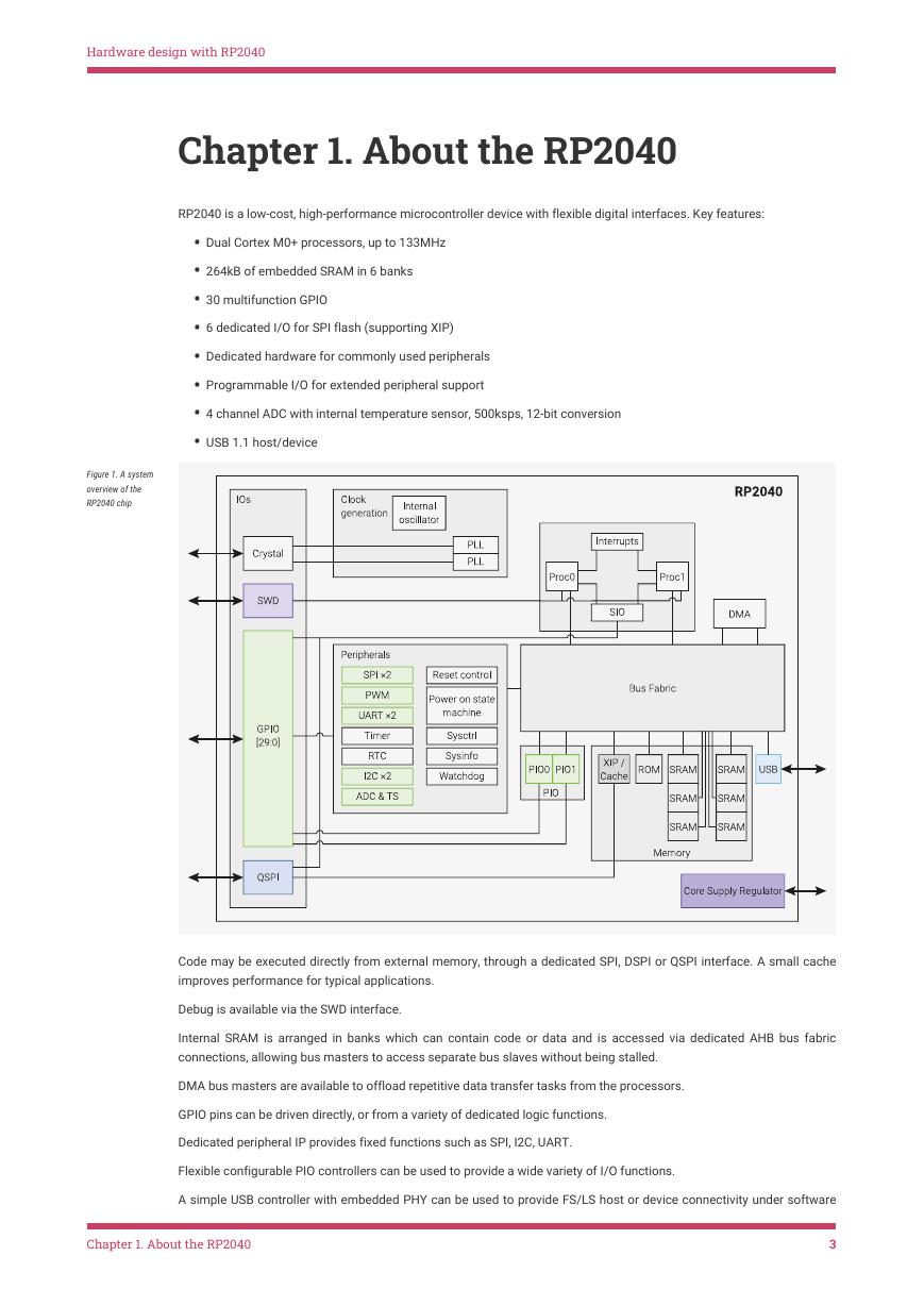
Figure 1. A system
overview of the
RP2040 chip
Code may be executed directly from external memory, through a dedicated SPI, DSPI or QSPI interface. A small cache
improves performance for typical applications.
Debug is available via the SWD interface.
Internal SRAM is arranged in banks which can contain code or data and is accessed via dedicated AHB bus fabric
connections, allowing bus masters to access separate bus slaves without being stalled.
DMA bus masters are available to offload repetitive data transfer tasks from the processors.
GPIO pins can be driven directly, or from a variety of dedicated logic functions.
Dedicated peripheral IP provides fixed functions such as SPI, I2C, UART.
Flexible configurable PIO controllers can be used to provide a wide variety of I/O functions.
A simple USB controller with embedded PHY can be used to provide FS/LS host or device connectivity under software
Chapter 1. About the RP2040
3
�
Hardware design with RP2040
control.
4 GPIOs also share package pins with ADC inputs.
2 PLLs are available to provide a USB or ADC fixed 48MHz clock, and a flexible system clock up to 133MHz
An internal voltage regulator will supply the core voltage so the end product only needs supply the I/O voltage.
Chapter 1. About the RP2040
4
�
Hardware design with RP2040
Chapter 2. Minimal design example
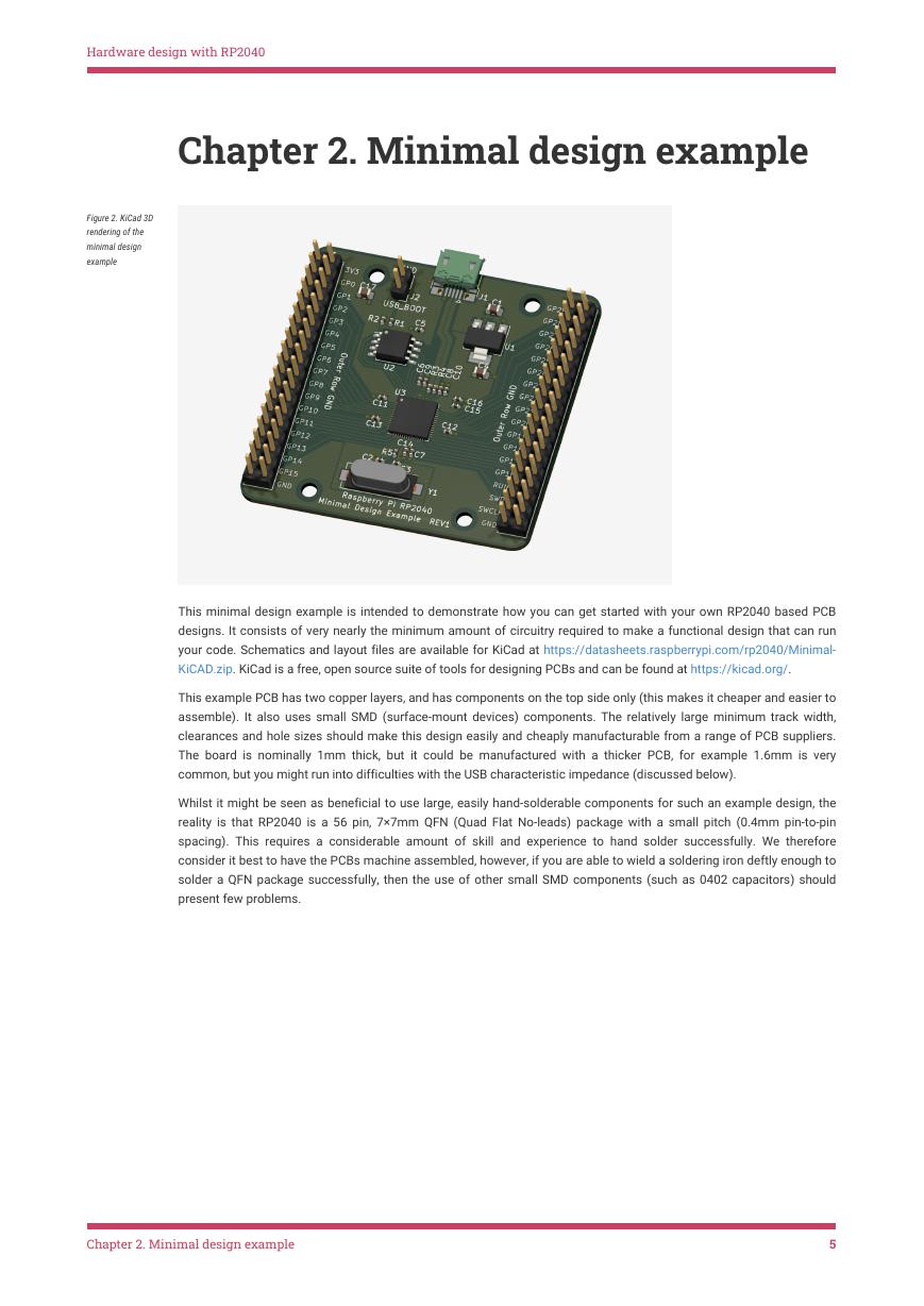
Figure 2. KiCad 3D
rendering of the
minimal design
example
This minimal design example is intended to demonstrate how you can get started with your own RP2040 based PCB
designs. It consists of very nearly the minimum amount of circuitry required to make a functional design that can run
your code. Schematics and layout files are available for KiCad at https://datasheets.raspberrypi.com/rp2040/Minimal-
KiCAD.zip. KiCad is a free, open source suite of tools for designing PCBs and can be found at https://kicad.org/.
This example PCB has two copper layers, and has components on the top side only (this makes it cheaper and easier to
assemble). It also uses small SMD (surface-mount devices) components. The relatively large minimum track width,
clearances and hole sizes should make this design easily and cheaply manufacturable from a range of PCB suppliers.
The board is nominally 1mm thick, but it could be manufactured with a thicker PCB, for example 1.6mm is very
common, but you might run into difficulties with the USB characteristic impedance (discussed below).
Whilst it might be seen as beneficial to use large, easily hand-solderable components for such an example design, the
reality is that RP2040 is a 56 pin, 7×7mm QFN (Quad Flat No-leads) package with a small pitch (0.4mm pin-to-pin
spacing). This requires a considerable amount of skill and experience to hand solder successfully. We therefore
consider it best to have the PCBs machine assembled, however, if you are able to wield a soldering iron deftly enough to
solder a QFN package successfully, then the use of other small SMD components (such as 0402 capacitors) should
present few problems.
Chapter 2. Minimal design example
5
�
Hardware design with RP2040
Figure 3. Schematic
section RP2040
connections
This design consists of four main elements: power, flash storage, crystal oscillator, and I/Os (input/outputs), and we’ll
consider each in turn below.
2.1. Power
At its simplest, RP2040 requires two different voltage supplies, 3.3V (for the I/O) and 1.1V (for the chip’s digital core).
Fortunately, there is an internal low-dropout voltage regulator (LDO) built into the device, which converts 3.3V to 1.1V for
us, so we don’t have to worry too much about the 1.1V supply.
2.1.1. Input supply
Figure 4. Schematic
section showing the
power input
The input power connection for this design is via the 5V VBUS pin of a Micro-USB connector (labelled J1 in Figure 4).
This is a common method of powering electronic devices, and it makes sense here, as RP2040 has USB functionality,
which we will be wiring to the data pins of this connector. As we need only 3.3V for this design, we need to lower the
incoming 5V USB supply, in this case, using a second, external LDO voltage regulator. The NCP1117 (U1) chosen here
has a fixed output of 3.3V, is widely available, and can provide up to 1A of current, which will be plenty for most designs.
A look at the datasheet for the NCP1117 tells us that this device requires a 10μF capacitor on the input, and another on
2.1. Power
6
�
Hardware design with RP2040
the output (C1 and C4).
2.1.2. Decoupling capacitors
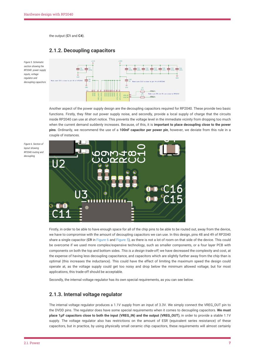
Figure 5. Schematic
section showing the
RP2040 power supply
inputs, voltage
regulator and
decoupling capacitors
Figure 6. Section of
layout showing
RP2040 routing and
decoupling
Another aspect of the power supply design are the decoupling capacitors required for RP2040. These provide two basic
functions. Firstly, they filter out power supply noise, and secondly, provide a local supply of charge that the circuits
inside RP2040 can use at short notice. This prevents the voltage level in the immediate vicinity from dropping too much
when the current demand suddenly increases. Because, of this, it is important to place decoupling close to the power
pins. Ordinarily, we recommend the use of a 100nF capacitor per power pin, however, we deviate from this rule in a
couple of instances.
Firstly, in order to be able to have enough space for all of the chip pins to be able to be routed out, away from the device,
we have to compromise with the amount of decoupling capacitors we can use. In this design, pins 48 and 49 of RP2040
share a single capacitor (C9 in Figure 6 and Figure 5), as there is not a lot of room on that side of the device. This could
be overcome if we used more complex/expensive technology, such as smaller components, or a four layer PCB with
components on both the top and bottom sides. This is a design trade-off; we have decreased the complexity and cost, at
the expense of having less decoupling capacitance, and capacitors which are slightly further away from the chip than is
optimal (this increases the inductance). This could have the effect of limiting the maximum speed the design could
operate at, as the voltage supply could get too noisy and drop below the minimum allowed voltage; but for most
applications, this trade-off should be acceptable.
Secondly, the internal voltage regulator has its own special requirements, as you can see below.
2.1.3. Internal voltage regulator
The internal voltage regulator produces a 1.1V supply from an input of 3.3V. We simply connect the VREG_OUT pin to
the DVDD pins. The regulator does have some special requirements when it comes to decoupling capacitors. We must
place 1μF capacitors close to both the input (VREG_IN) and the output (VREG_OUT), in order to provide a stable 1.1V
supply. The voltage regulator also has restrictions on the amount of ESR (equivalent series resistance) of these
capacitors, but in practice, by using physically small ceramic chip capacitors, these requirements will almost certainly
2.1. Power
7
�





 V2版本原理图(Capacitive-Fingerprint-Reader-Schematic_V2).pdf
 摄像头工作原理.doc
 VL53L0X简要说明(En.FLVL53L00216).pdf
 原理图(DVK720-Schematic).pdf
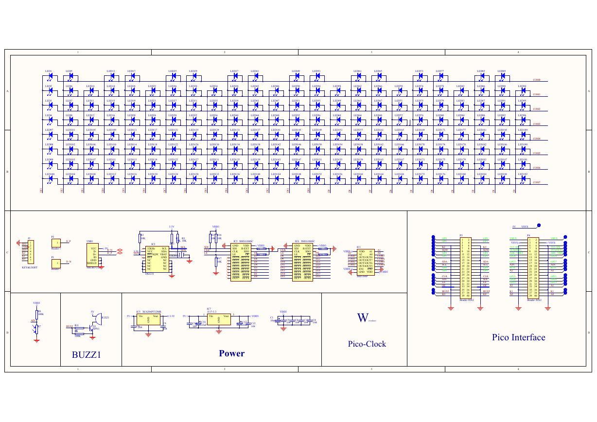 原理图(Pico-Clock-Green-Schdoc).pdf
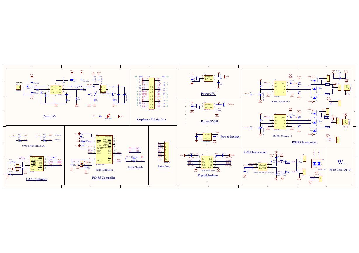 原理图(RS485-CAN-HAT-B-schematic).pdf
 File:SIM7500_SIM7600_SIM7800 Series_SSL_Application Note_V2.00.pdf
 ADS1263(Ads1262).pdf
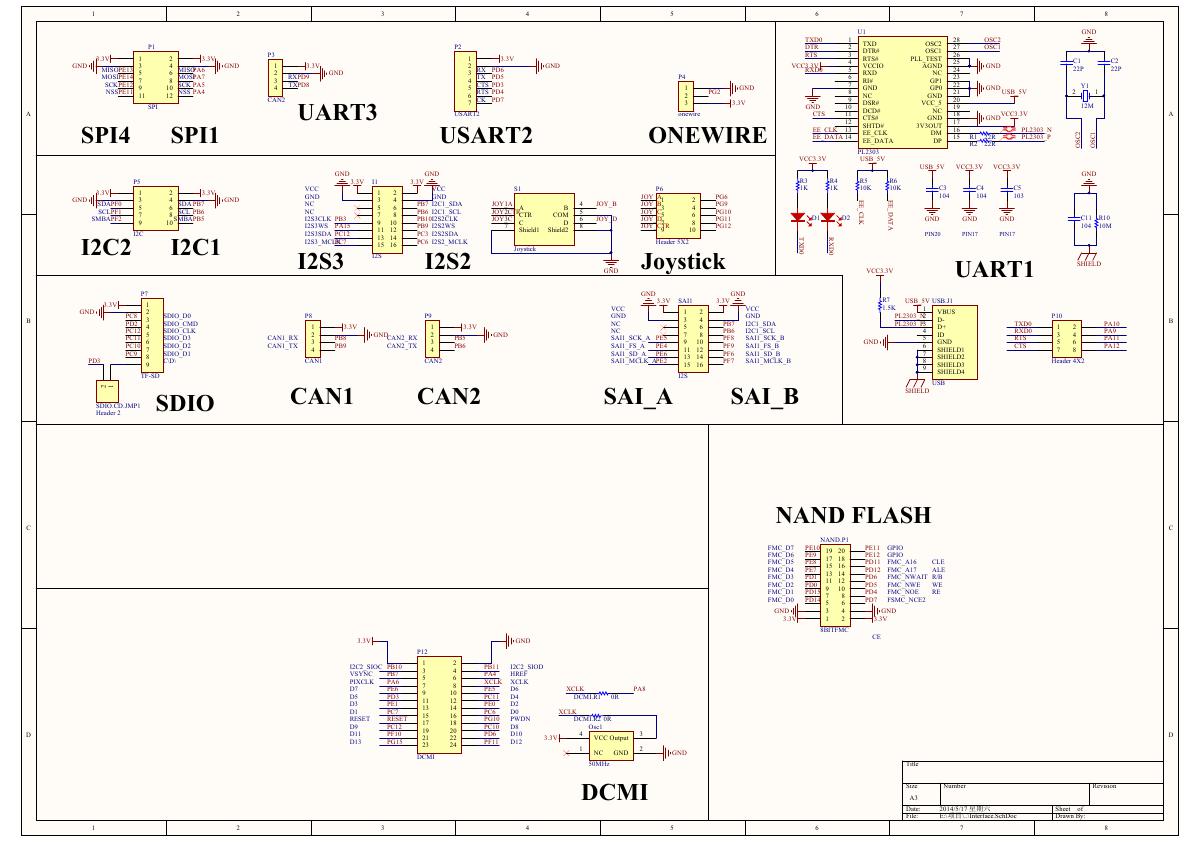 原理图(Open429Z-D-Schematic).pdf
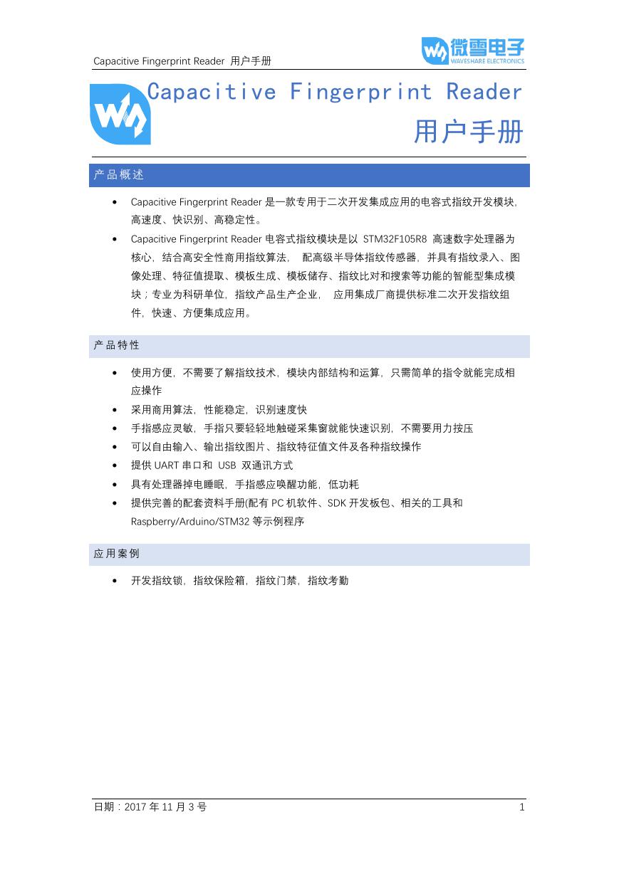 用户手册(Capacitive_Fingerprint_Reader_User_Manual_CN).pdf
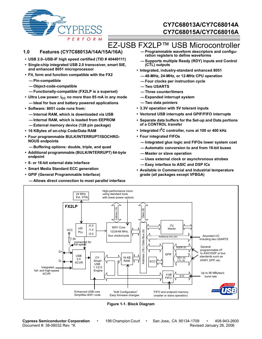 CY7C68013A(英文版)(CY7C68013A).pdf
 TechnicalReference_Dem.pdf