S-8254A Series
BATTERY PROTECTION IC
FOR 3-SERIAL- OR 4-SERIAL-CELL PACK
Rev.5.0_01
www.sii-ic.com
© Seiko Instruments Inc., 2002-2010
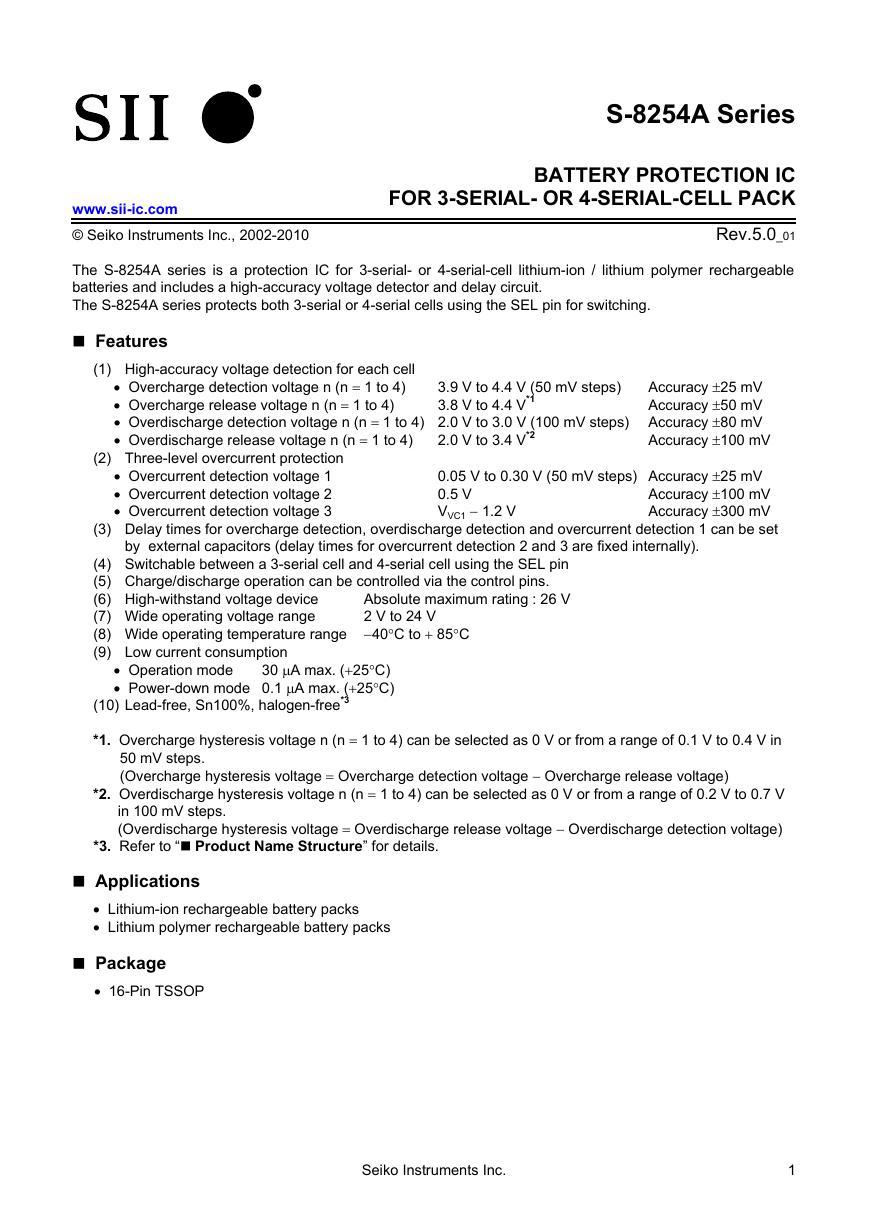
The S-8254A series is a protection IC for 3-serial- or 4-serial-cell lithium-ion / lithium polymer rechargeable
batteries and includes a high-accuracy voltage detector and delay circuit.
The S-8254A series protects both 3-serial or 4-serial cells using the SEL pin for switching.
Features
(1) High-accuracy voltage detection for each cell
Accuracy ±25 mV
• Overcharge detection voltage n (n = 1 to 4)
Accuracy ±50 mV
• Overcharge release voltage n (n = 1 to 4)
• Overdischarge detection voltage n (n = 1 to 4) 2.0 V to 3.0 V (100 mV steps) Accuracy ±80 mV
Accuracy ±100 mV
• Overdischarge release voltage n (n = 1 to 4)
3.9 V to 4.4 V (50 mV steps)
3.8 V to 4.4 V*1
2.0 V to 3.4 V*2
(2) Three-level overcurrent protection
• Overcurrent detection voltage 1
• Overcurrent detection voltage 2
• Overcurrent detection voltage 3
0.05 V to 0.30 V (50 mV steps) Accuracy ±25 mV
Accuracy ±100 mV
0.5 V
VVC1 − 1.2 V
Accuracy ±300 mV
(3) Delay times for overcharge detection, overdischarge detection and overcurrent detection 1 can be set
by external capacitors (delay times for overcurrent detection 2 and 3 are fixed internally).
(4) Switchable between a 3-serial cell and 4-serial cell using the SEL pin
(5) Charge/discharge operation can be controlled via the control pins.
(6) High-withstand voltage device
(7) Wide operating voltage range
(8) Wide operating temperature range −40°C to + 85°C
(9) Low current consumption
Absolute maximum rating : 26 V
2 V to 24 V
• Operation mode
30 μA max. (+25°C)
• Power-down mode 0.1 μA max. (+25°C)
(10) Lead-free, Sn100%, halogen-free*3
*1. Overcharge hysteresis voltage n (n = 1 to 4) can be selected as 0 V or from a range of 0.1 V to 0.4 V in
50 mV steps.
(Overcharge hysteresis voltage = Overcharge detection voltage − Overcharge release voltage)
*2. Overdischarge hysteresis voltage n (n = 1 to 4) can be selected as 0 V or from a range of 0.2 V to 0.7 V
in 100 mV steps.
(Overdischarge hysteresis voltage = Overdischarge release voltage − Overdischarge detection voltage)
*3. Refer to “ Product Name Structure” for details.
Applications
• Lithium-ion rechargeable battery packs
• Lithium polymer rechargeable battery packs
Package
• 16-Pin TSSOP
Seiko Instruments Inc.
1
�
BATTERY PROTECTION IC FOR 3-SERIAL- OR 4-SERIAL-CELL PACK
S-8254A Series
Rev.5.0_01
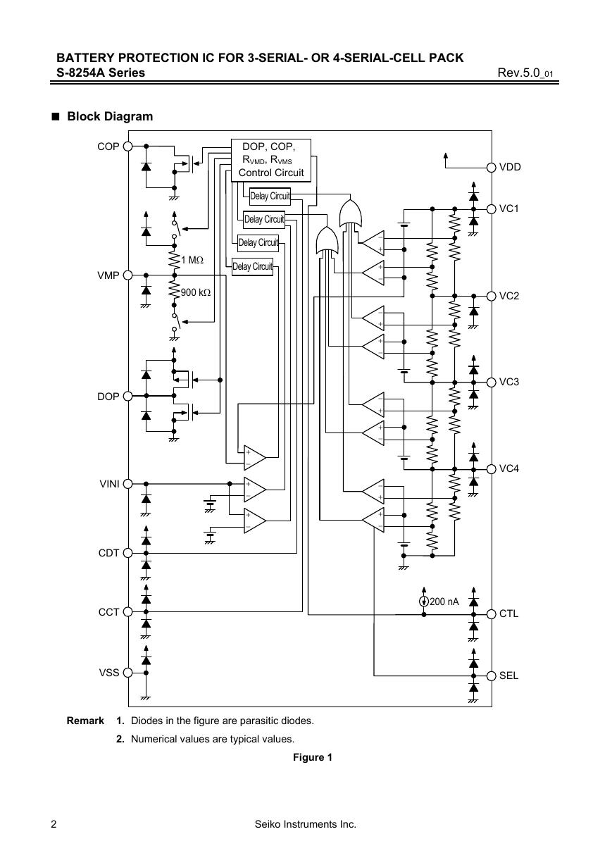
Block Diagram
DOP, COP,
RVMD, RVMS
Control Circuit
Delay Circuit
Delay Circuit
Delay Circuit
Delay Circuit
1 MΩ
900 kΩ
+
−
+
−
+
−
−
+
+
−
−
+
+
−
−
+
+
−
−
+
+
−
COP
VMP
DOP
VINI
CDT
CCT
VSS
Remark 1. Diodes in the figure are parasitic diodes.
2. Numerical values are typical values.
Figure 1
Seiko Instruments Inc.
2
VDD
VC1
VC2
VC3
VC4
CTL
SEL
200 nA
�
Rev.5.0_01
BATTERY PROTECTION IC FOR 3-SERIAL- OR 4-SERIAL-CELL PACK
S-8254A Series
Product Name Structure
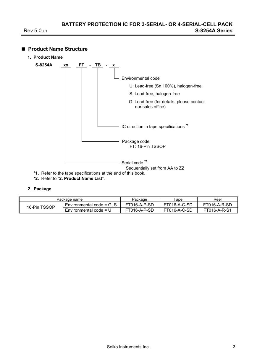
1. Product Name
S-8254A
xx
FT
- TB
-
x
Environmental code
U: Lead-free (Sn 100%), halogen-free
S: Lead-free, halogen-free
G: Lead-free (for details, please contact
our sales office)
IC direction in tape specifications *1
Package code
FT: 16-Pin TSSOP
*1. Refer to the tape specifications at the end of this book.
*2. Refer to “2. Product Name List”.
Serial code *2
Sequentially set from AA to ZZ
2. Package
Package name
16-Pin TSSOP
Environmental code = G, S
Environmental code = U
Package
FT016-A-P-SD
FT016-A-P-SD
Tape
Reel
FT016-A-C-SD
FT016-A-C-SD
FT016-A-R-SD
FT016-A-R-S1
Seiko Instruments Inc.
3
�
BATTERY PROTECTION IC FOR 3-SERIAL- OR 4-SERIAL-CELL PACK
S-8254A Series
Rev.5.0_01
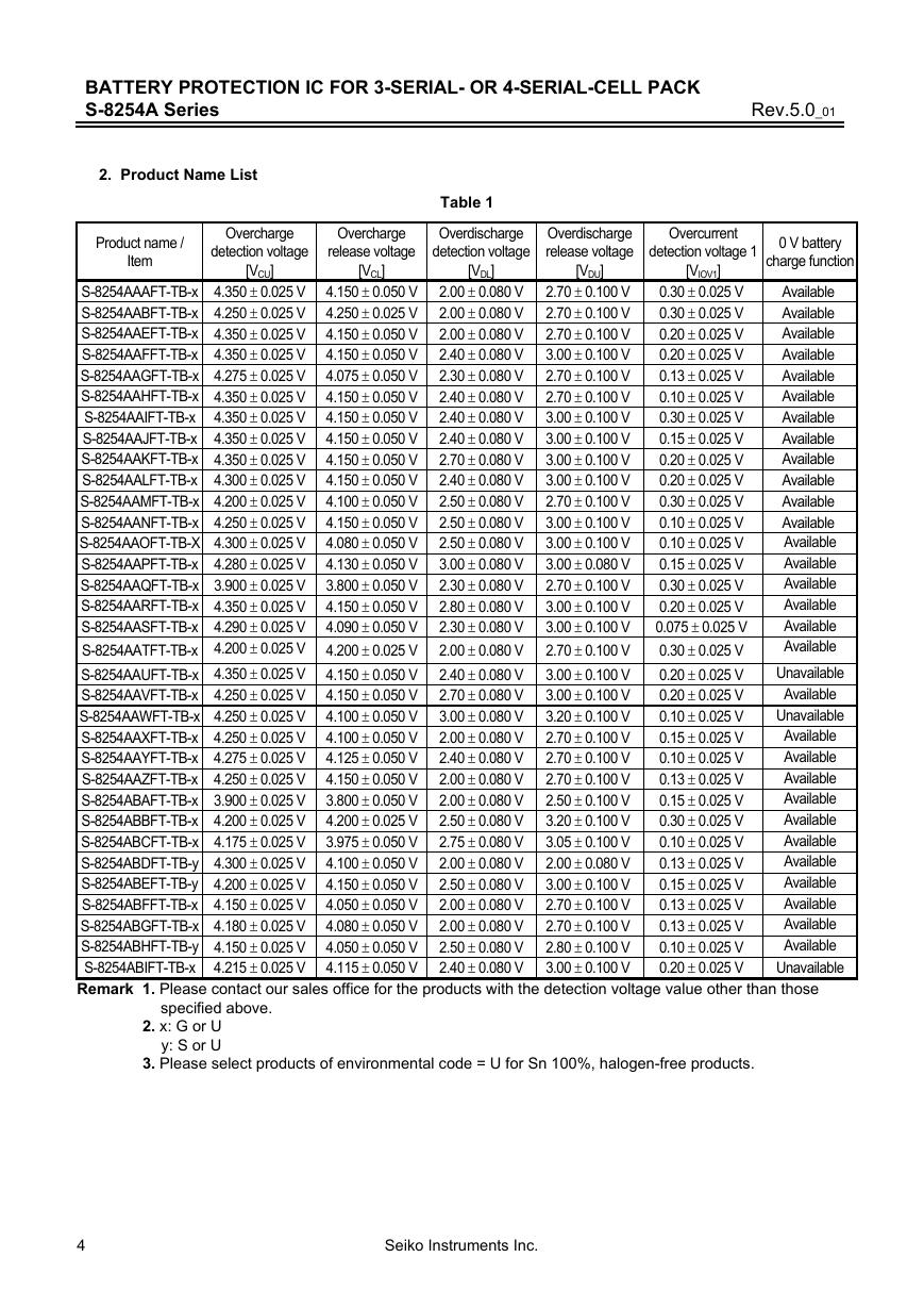
2. Product Name List
Product name /
Item
Overcharge
detection voltage
Overcharge
release voltage
[VCU]
[VCL]
Table 1
Overdischarge
detection voltage
[VDL]
Overdischarge
release voltage
Overcurrent
detection voltage 1
[VDU]
[VIOV1]
0 V battery
charge function
S-8254AAAFT-TB-x 4.350 ± 0.025 V
S-8254AABFT-TB-x 4.250 ± 0.025 V
S-8254AAEFT-TB-x 4.350 ± 0.025 V
S-8254AAFFT-TB-x 4.350 ± 0.025 V
S-8254AAGFT-TB-x 4.275 ± 0.025 V
S-8254AAHFT-TB-x 4.350 ± 0.025 V
S-8254AAIFT-TB-x 4.350 ± 0.025 V
S-8254AAJFT-TB-x 4.350 ± 0.025 V
S-8254AAKFT-TB-x 4.350 ± 0.025 V
S-8254AALFT-TB-x 4.300 ± 0.025 V
S-8254AAMFT-TB-x 4.200 ± 0.025 V
S-8254AANFT-TB-x 4.250 ± 0.025 V
S-8254AAOFT-TB-X 4.300 ± 0.025 V
S-8254AAPFT-TB-x 4.280 ± 0.025 V
S-8254AAQFT-TB-x 3.900 ± 0.025 V
S-8254AARFT-TB-x 4.350 ± 0.025 V
S-8254AASFT-TB-x 4.290 ± 0.025 V
S-8254AATFT-TB-x 4.200 ± 0.025 V
S-8254AAUFT-TB-x 4.350 ± 0.025 V
S-8254AAVFT-TB-x 4.250 ± 0.025 V
S-8254AAWFT-TB-x 4.250 ± 0.025 V
S-8254AAXFT-TB-x 4.250 ± 0.025 V
S-8254AAYFT-TB-x 4.275 ± 0.025 V
S-8254AAZFT-TB-x 4.250 ± 0.025 V
S-8254ABAFT-TB-x 3.900 ± 0.025 V
S-8254ABBFT-TB-x 4.200 ± 0.025 V
S-8254ABCFT-TB-x 4.175 ± 0.025 V
S-8254ABDFT-TB-y 4.300 ± 0.025 V
S-8254ABEFT-TB-y 4.200 ± 0.025 V
S-8254ABFFT-TB-x 4.150 ± 0.025 V
S-8254ABGFT-TB-x 4.180 ± 0.025 V
S-8254ABHFT-TB-y 4.150 ± 0.025 V
S-8254ABIFT-TB-x 4.215 ± 0.025 V
Remark 1. Please contact our sales office for the products with the detection voltage value other than those
4.150 ± 0.050 V
4.250 ± 0.025 V
4.150 ± 0.050 V
4.150 ± 0.050 V
4.075 ± 0.050 V
4.150 ± 0.050 V
4.150 ± 0.050 V
4.150 ± 0.050 V
4.150 ± 0.050 V
4.150 ± 0.050 V
4.100 ± 0.050 V
4.150 ± 0.050 V
4.080 ± 0.050 V
4.130 ± 0.050 V
3.800 ± 0.050 V
4.150 ± 0.050 V
4.090 ± 0.050 V
4.200 ± 0.025 V
4.150 ± 0.050 V
4.150 ± 0.050 V
4.100 ± 0.050 V
4.100 ± 0.050 V
4.125 ± 0.050 V
4.150 ± 0.050 V
3.800 ± 0.050 V
4.200 ± 0.025 V
3.975 ± 0.050 V
4.100 ± 0.050 V
4.150 ± 0.050 V
4.050 ± 0.050 V
4.080 ± 0.050 V
4.050 ± 0.050 V
4.115 ± 0.050 V
0.30 ± 0.025 V
0.30 ± 0.025 V
0.20 ± 0.025 V
0.20 ± 0.025 V
0.13 ± 0.025 V
0.10 ± 0.025 V
0.30 ± 0.025 V
0.15 ± 0.025 V
0.20 ± 0.025 V
0.20 ± 0.025 V
0.30 ± 0.025 V
0.10 ± 0.025 V
0.10 ± 0.025 V
0.15 ± 0.025 V
0.30 ± 0.025 V
0.20 ± 0.025 V
0.075 ± 0.025 V
0.30 ± 0.025 V
0.20 ± 0.025 V
0.20 ± 0.025 V
0.10 ± 0.025 V
0.15 ± 0.025 V
0.10 ± 0.025 V
0.13 ± 0.025 V
0.15 ± 0.025 V
0.30 ± 0.025 V
0.10 ± 0.025 V
0.13 ± 0.025 V
0.15 ± 0.025 V
0.13 ± 0.025 V
0.13 ± 0.025 V
0.10 ± 0.025 V
0.20 ± 0.025 V
2.00 ± 0.080 V
2.00 ± 0.080 V
2.00 ± 0.080 V
2.40 ± 0.080 V
2.30 ± 0.080 V
2.40 ± 0.080 V
2.40 ± 0.080 V
2.40 ± 0.080 V
2.70 ± 0.080 V
2.40 ± 0.080 V
2.50 ± 0.080 V
2.50 ± 0.080 V
2.50 ± 0.080 V
3.00 ± 0.080 V
2.30 ± 0.080 V
2.80 ± 0.080 V
2.30 ± 0.080 V
2.00 ± 0.080 V
2.40 ± 0.080 V
2.70 ± 0.080 V
3.00 ± 0.080 V
2.00 ± 0.080 V
2.40 ± 0.080 V
2.00 ± 0.080 V
2.00 ± 0.080 V
2.50 ± 0.080 V
2.75 ± 0.080 V
2.00 ± 0.080 V
2.50 ± 0.080 V
2.00 ± 0.080 V
2.00 ± 0.080 V
2.50 ± 0.080 V
2.40 ± 0.080 V
2.70 ± 0.100 V
2.70 ± 0.100 V
2.70 ± 0.100 V
3.00 ± 0.100 V
2.70 ± 0.100 V
2.70 ± 0.100 V
3.00 ± 0.100 V
3.00 ± 0.100 V
3.00 ± 0.100 V
3.00 ± 0.100 V
2.70 ± 0.100 V
3.00 ± 0.100 V
3.00 ± 0.100 V
3.00 ± 0.080 V
2.70 ± 0.100 V
3.00 ± 0.100 V
3.00 ± 0.100 V
2.70 ± 0.100 V
3.00 ± 0.100 V
3.00 ± 0.100 V
3.20 ± 0.100 V
2.70 ± 0.100 V
2.70 ± 0.100 V
2.70 ± 0.100 V
2.50 ± 0.100 V
3.20 ± 0.100 V
3.05 ± 0.100 V
2.00 ± 0.080 V
3.00 ± 0.100 V
2.70 ± 0.100 V
2.70 ± 0.100 V
2.80 ± 0.100 V
3.00 ± 0.100 V
Available
Available
Available
Available
Available
Available
Available
Available
Available
Available
Available
Available
Available
Available
Available
Available
Available
Available
Unavailable
Available
Unavailable
Available
Available
Available
Available
Available
Available
Available
Available
Available
Available
Available
Unavailable
specified above.
2. x: G or U
y: S or U
3. Please select products of environmental code = U for Sn 100%, halogen-free products.
4
Seiko Instruments Inc.
�
Rev.5.0_01
BATTERY PROTECTION IC FOR 3-SERIAL- OR 4-SERIAL-CELL PACK
S-8254A Series
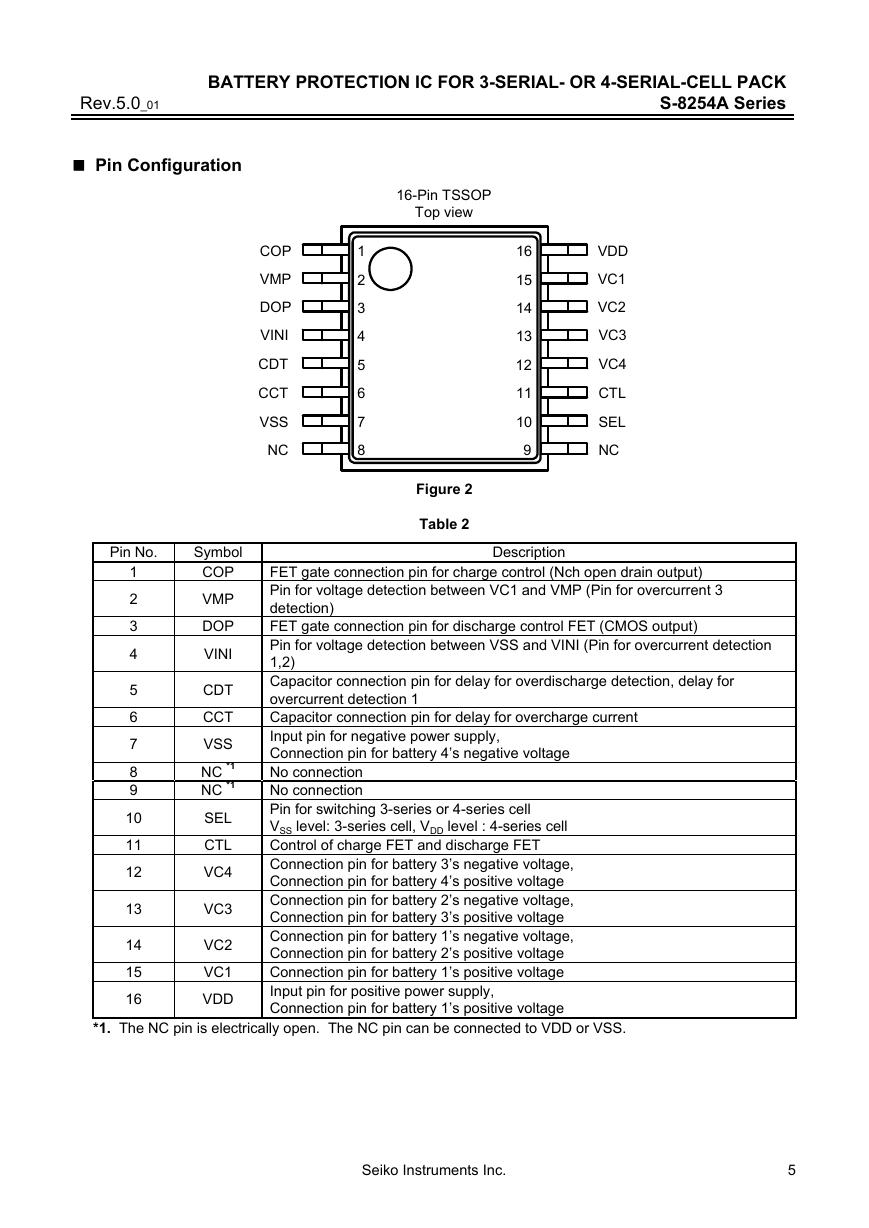
Pin Configuration
COP
VMP
DOP
VINI
CDT
CCT
VSS
NC
1
2
3
4
5
6
7
8
16-Pin TSSOP
Top view
16
15
14
13
12
11
10
9
VDD
VC1
VC2
VC3
VC4
CTL
SEL
NC
Figure 2
Table 2
Description
Pin No.
1
2
3
4
5
6
7
8
9
10
11
12
13
14
15
16
Symbol
COP
VMP
DOP
VINI
CDT
CCT
VSS
NC *1
NC *1
SEL
CTL
VC4
VC3
VC2
VC1
VDD
FET gate connection pin for charge control (Nch open drain output)
Pin for voltage detection between VC1 and VMP (Pin for overcurrent 3
detection)
FET gate connection pin for discharge control FET (CMOS output)
Pin for voltage detection between VSS and VINI (Pin for overcurrent detection
1,2)
Capacitor connection pin for delay for overdischarge detection, delay for
overcurrent detection 1
Capacitor connection pin for delay for overcharge current
Input pin for negative power supply,
Connection pin for battery 4’s negative voltage
No connection
No connection
Pin for switching 3-series or 4-series cell
VSS level: 3-series cell, VDD level : 4-series cell
Control of charge FET and discharge FET
Connection pin for battery 3’s negative voltage,
Connection pin for battery 4’s positive voltage
Connection pin for battery 2’s negative voltage,
Connection pin for battery 3’s positive voltage
Connection pin for battery 1’s negative voltage,
Connection pin for battery 2’s positive voltage
Connection pin for battery 1’s positive voltage
Input pin for positive power supply,
Connection pin for battery 1’s positive voltage
*1. The NC pin is electrically open. The NC pin can be connected to VDD or VSS.
Seiko Instruments Inc.
5
�
BATTERY PROTECTION IC FOR 3-SERIAL- OR 4-SERIAL-CELL PACK
S-8254A Series
Rev.5.0_01
Absolute Maximum Ratings
Item
Input voltage between VDD and VSS
Input pin voltage
VMP pin input voltage
DOP pin output voltage
COP pin output voltage
Power dissipation
Symbol
VDS
VIN
VVMP
VDOP
VCOP
PD
Topr
Tstg
Table 3
Applied pin
⎯
VC1, VC2, VC3,
VC4, CTL, SEL,
CCT, CDT, VINI
(Ta = 25°C unless otherwise specified)
Absolute Maximum Ratings
VSS − 0.3 to VSS + 26
Unit
V
VSS − 0.3 to VDD + 0.3
V
VMP
DOP
COP
⎯
⎯
⎯
⎯
VSS − 0.3 to VSS + 26
VSS − 0.3 to VDD + 0.3
VSS − 0.3 to VSS + 26
V
V
V
400 (When not mounted on board) mW
mW
°C
°C
1100*1
Operating ambient temperature
Storage temperature
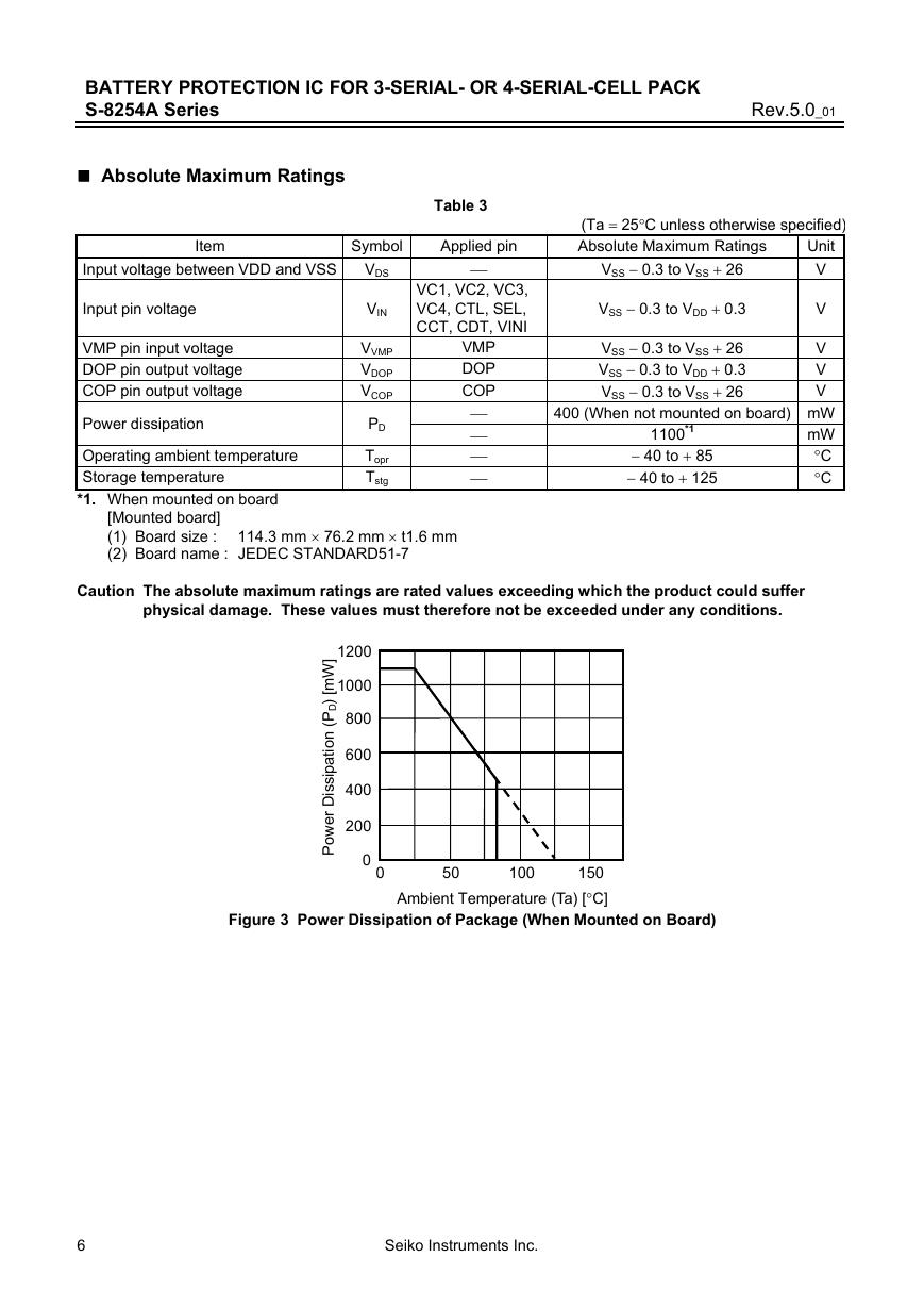
*1. When mounted on board
Caution The absolute maximum ratings are rated values exceeding which the product could suffer
[Mounted board]
(1) Board size : 114.3 mm × 76.2 mm × t1.6 mm
(2) Board name : JEDEC STANDARD51-7
− 40 to + 85
− 40 to + 125
physical damage. These values must therefore not be exceeded under any conditions.
1200
1000
800
600
400
]
W
m
[
)
D
P
(
n
o
i
t
i
a
p
s
s
D
i
r
e
w
o
200
0 P
0
50
150
Ambient Temperature (Ta) [°C]
100
Figure 3 Power Dissipation of Package (When Mounted on Board)
6
Seiko Instruments Inc.
�
Rev.5.0_01
BATTERY PROTECTION IC FOR 3-SERIAL- OR 4-SERIAL-CELL PACK
S-8254A Series
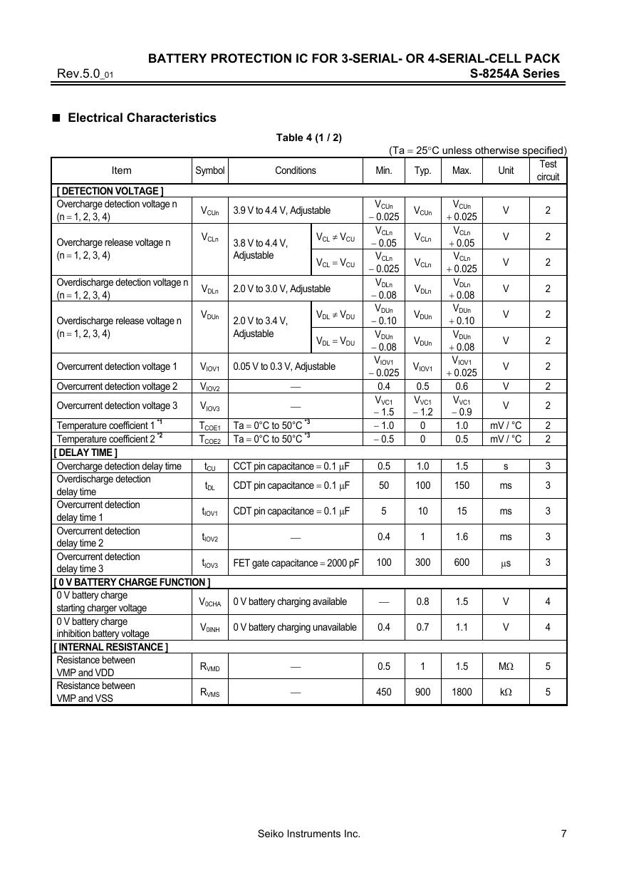
Electrical Characteristics
Table 4 (1 / 2)
(Ta = 25°C unless otherwise specified)
Item
Symbol
Conditions
Min.
Typ.
Max.
Unit
[ DETECTION VOLTAGE ]
Overcharge detection voltage n
(n = 1, 2, 3, 4)
Overcharge release voltage n
(n = 1, 2, 3, 4)
Overdischarge detection voltage n
(n = 1, 2, 3, 4)
Overdischarge release voltage n
(n = 1, 2, 3, 4)
3.9 V to 4.4 V, Adjustable
3.8 V to 4.4 V,
Adjustable
VCL ≠ VCU
VCL = VCU
2.0 V to 3.0 V, Adjustable
2.0 V to 3.4 V,
Adjustable
VDL ≠ VDU
VDL = VDU
VCUn
VCLn
VDLn
VDUn
VCLn
VDLn
VCUn
− 0.025 VCUn
VCLn
VCLn
− 0.05
VCLn
− 0.025
VDLn
− 0.08
VDUn
− 0.10
VDUn
− 0.08
VIOV1
− 0.025 VIOV1
0.4
0.5
VVC1
VVC1
− 1.5
− 1.2
− 1.0
− 0.5
VDUn
VDUn
0
0
1.0
100
VCUn
+ 0.025
VCLn
+ 0.05
VCLn
+ 0.025
VDLn
+ 0.08
VDUn
+ 0.10
VDUn
+ 0.08
VIOV1
+ 0.025
0.6
VVC1
− 0.9
1.0
0.5
1.5
150
5
0.4
100
⎯
0.4
0.5
10
1
15
1.6
300
600
0.8
0.7
1
1.5
1.1
1.5
450
900
1800
V
V
V
V
V
V
V
V
V
mV / °C
mV / °C
s
ms
ms
ms
μs
V
V
MΩ
kΩ
Test
circuit
2
2
2
2
2
2
2
2
2
2
2
3
3
3
3
3
4
4
5
5
Overcurrent detection voltage 1
Overcurrent detection voltage 2
Overcurrent detection voltage 3
Temperature coefficient 1 *1
Temperature coefficient 2 *2
[ DELAY TIME ]
Overcharge detection delay time
Overdischarge detection
delay time
Overcurrent detection
delay time 1
Overcurrent detection
delay time 2
Overcurrent detection
delay time 3
[ 0 V BATTERY CHARGE FUNCTION ]
0 V battery charge
starting charger voltage
0 V battery charge
inhibition battery voltage
[ INTERNAL RESISTANCE ]
Resistance between
VMP and VDD
Resistance between
VMP and VSS
0.05 V to 0.3 V, Adjustable
VIOV1
VIOV2
VIOV3
TCOE1 Ta = 0°C to 50°C *3
TCOE2 Ta = 0°C to 50°C *3
⎯
⎯
tCU
tDL
CCT pin capacitance = 0.1 μF
CDT pin capacitance = 0.1 μF
0.5
50
tIOV1 CDT pin capacitance = 0.1 μF
tIOV2
tIOV3
⎯
FET gate capacitance = 2000 pF
V0CHA 0 V battery charging available
V0INH
RVMD
RVMS
0 V battery charging unavailable
⎯
⎯
Seiko Instruments Inc.
7
�
BATTERY PROTECTION IC FOR 3-SERIAL- OR 4-SERIAL-CELL PACK
S-8254A Series
Rev.5.0_01
Item
[ INPUT VOLTAGE ]
Operating voltage between VDD
and VSS
CTL input voltage “H”
CTL input voltage “L”
SEL input voltage “H”
SEL input voltage “L”
[ INPUT CURRENT ]
Current consumption
on operation
Current consumption
at power down
VC1 pin current
VC2 pin current
VC3 pin current
VC4 pin current
CTL pin current “H”
CTL pin current “L”
SEL pin current “H”
Table 4 (2 / 2)
Symbol
Conditions
VDSOP Output voltage of DOP and
COP fixed
VCTLH
VCTLL
VSELH
VSELL
IOPE
⎯
⎯
⎯
⎯
V1 = V2 = V3 = V4 = 3.5 V
IPDN
V1 = V2 = V3 = V4 = 1.5 V
IVC1
V1 = V2 = V3 = V4 = 3.5 V
IVC2
V1 = V2 = V3 = V4 = 3.5 V
IVC3
V1 = V2 = V3 = V4 = 3.5 V
IVC4
V1 = V2 = V3 = V4 = 3.5 V
ICTLH V1 = V2 = V3 = V4 = 3.5 V,
ICTLL V1 = V2 = V3 = V4 = 3.5 V,
ISELH V1 = V2 = V3 = V4 = 3.5 V,
ISELL V1 = V2 = V3 = V4 = 3.5 V,
VSEL = VDD
VCTL = VDD
VCTL = VSS
Min.
2
VDD
× 0.8
⎯
VDD
× 0.8
⎯
⎯
⎯
⎯
− 0.3
− 0.3
− 0.3
⎯
⎯
⎯
⎯
⎯
⎯
12
⎯
1.5
0
0
0
⎯
− 0.4
− 0.2
⎯
⎯
− 0.1
(Ta = 25°C unless otherwise specified)
Typ.
Max.
Unit
Test
circuit
24
⎯
VDD
× 0.2
⎯
VDD
× 0.2
30
0.1
3
0.3
0.3
0.3
0.1
⎯
0.1
V
V
V
V
V
μA
μA
μA
μA
μA
μA
μA
μA
μA
2
2
2
2
2
1
1
5
5
5
5
5
5
5
SEL pin current “L”
[ OUTPUT CURRENT ]
COP pin leakage current
COP pin sink current
DOP pin source current
DOP pin sink current
*1. Voltage temperature coefficient 1 : Overcharge detection voltage
*2. Voltage temperature coefficient 2 : Overcurrent detection voltage 1
*3. Since products are not screened at high and low temperature, the specification for this temperature range is
guaranteed by design, not tested in production.
VSEL = VSS
VCOP = 24 V
VCOP = VSS + 0.5 V
VDOP = VDD − 0.5 V
VDOP = VSS + 0.5 V
⎯
0.1
⎯
⎯
⎯
μA
μA
μA
μA
μA
⎯
⎯
⎯
⎯
⎯
ICOH
ICOL
IDOH
IDOL
⎯
10
10
10
5
5
5
5
5
8
Seiko Instruments Inc.
�


 V2版本原理图(Capacitive-Fingerprint-Reader-Schematic_V2).pdf
 摄像头工作原理.doc
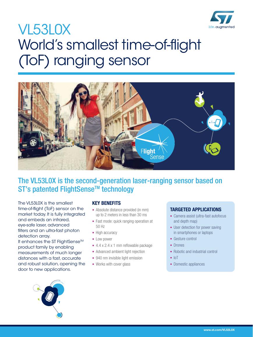 VL53L0X简要说明(En.FLVL53L00216).pdf
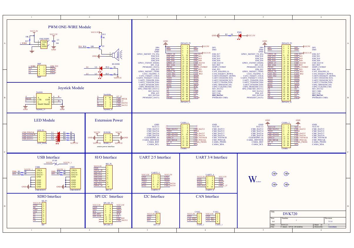 原理图(DVK720-Schematic).pdf
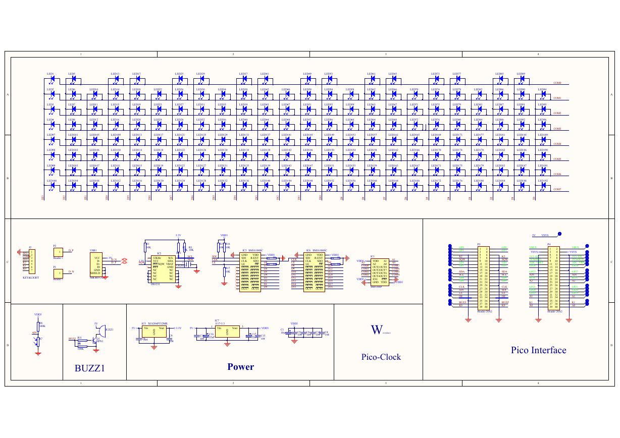 原理图(Pico-Clock-Green-Schdoc).pdf
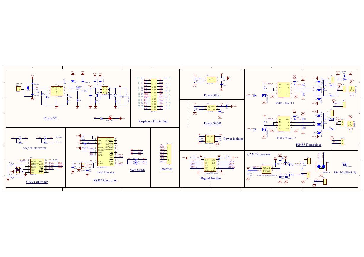 原理图(RS485-CAN-HAT-B-schematic).pdf
 File:SIM7500_SIM7600_SIM7800 Series_SSL_Application Note_V2.00.pdf
 ADS1263(Ads1262).pdf
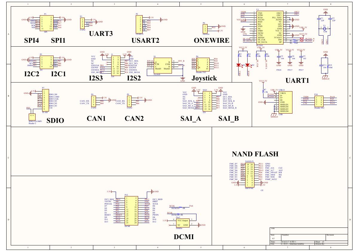 原理图(Open429Z-D-Schematic).pdf
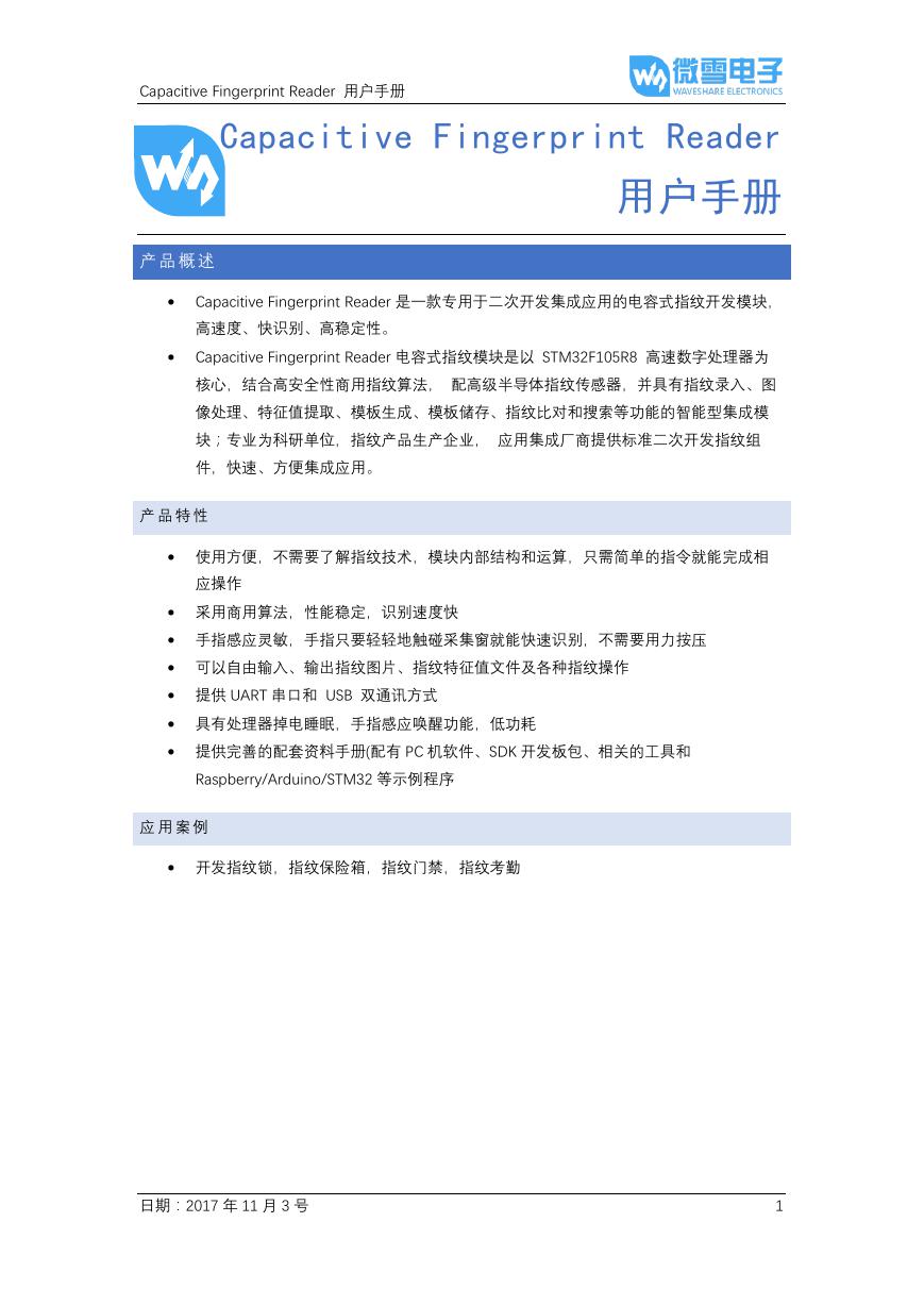 用户手册(Capacitive_Fingerprint_Reader_User_Manual_CN).pdf
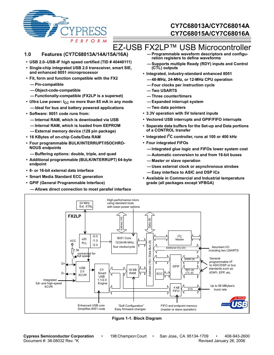 CY7C68013A(英文版)(CY7C68013A).pdf
 TechnicalReference_Dem.pdf