RM520N-GL
Hardware Design
5G Module Series
Version: 1.0
Date: 2022-07-15
Status: Released
RM520N-GL_Hardware_Design 1 / 84
�
5G Module Series
At Quectel, our aim is to provide timely and comprehensive services to our customers. If you
require any assistance, please contact our headquarters:
Quectel Wireless Solutions Co., Ltd.
Building 5, Shanghai Business Park Phase III (Area B), No.1016 Tianlin Road, Minhang District, Shanghai
200233, China
Tel: +86 21 5108 6236
Email: info@quectel.com
Or our local offices. For more information, please visit:
http://www.quectel.com/support/sales.htm.
For technical support, or to report documentation errors, please visit:
http://www.quectel.com/support/technical.htm.
Or email us at: support@quectel.com.
Legal Notices
We offer information as a service to you. The provided information is based on your requirements and we
make every effort to ensure its quality. You agree that you are responsible for using independent analysis
and evaluation in designing intended products, and we provide reference designs for illustrative purposes
only. Before using any hardware, software or service guided by this document, please read this notice
carefully. Even though we employ commercially reasonable efforts to provide the best possible
experience, you hereby acknowledge and agree that this document and related services hereunder are
provided to you on an “as available” basis. We may revise or restate this document from time to time at
our sole discretion without any prior notice to you.
Use and Disclosure Restrictions
License Agreements
Documents and information provided by us shall be kept confidential, unless specific permission is
granted. They shall not be accessed or used for any purpose except as expressly provided herein.
Copyright
Our and third-party products hereunder may contain copyrighted material. Such copyrighted material
shall not be copied, reproduced, distributed, merged, published, translated, or modified without prior
written consent. We and the third party have exclusive rights over copyrighted material. No license shall
be granted or conveyed under any patents, copyrights, trademarks, or service mark rights. To avoid
ambiguities, purchasing in any form cannot be deemed as granting a license other than the normal
non-exclusive, royalty-free license to use the material. We reserve the right to take legal action for
noncompliance with abovementioned requirements, unauthorized use, or other illegal or malicious use of
the material.
RM520N-GL_Hardware_Design 1 / 84
�
5G Module Series
Trademarks
Except as otherwise set forth herein, nothing in this document shall be construed as conferring any rights
to use any trademark, trade name or name, abbreviation, or counterfeit product thereof owned by Quectel
or any third party in advertising, publicity, or other aspects.
Third-Party Rights
This document may refer to hardware, software and/or documentation owned by one or more third parties
(“third-party materials”). Use of such third-party materials shall be governed by all restrictions and
obligations applicable thereto.
We make no warranty or representation, either express or implied, regarding the third-party materials,
including but not limited to any implied or statutory, warranties of merchantability or fitness for a particular
purpose, quiet enjoyment, system integration, information accuracy, and non-infringement of any
third-party intellectual property rights with regard to the licensed technology or use thereof. Nothing herein
constitutes a representation or warranty by us to either develop, enhance, modify, distribute, market, sell,
offer for sale, or otherwise maintain production of any our products or any other hardware, software,
device, tool, information, or product. We moreover disclaim any and all warranties arising from the course
of dealing or usage of trade.
Privacy Policy
To implement module functionality, certain device data are uploaded to Quectel’s or third-party’s servers,
including carriers, chipset suppliers or customer-designated servers. Quectel, strictly abiding by the
relevant laws and regulations, shall retain, use, disclose or otherwise process relevant data for the
purpose of performing the service only or as permitted by applicable laws. Before data interaction with
third parties, please be informed of their privacy and data security policy.
Disclaimer
a) We acknowledge no liability for any injury or damage arising from the reliance upon the information.
b) We shall bear no liability resulting from any inaccuracies or omissions, or from the use of the
information contained herein.
c) While we have made every effort to ensure that the functions and features under development are
free from errors, it is possible that they could contain errors, inaccuracies, and omissions. Unless
otherwise provided by valid agreement, we make no warranties of any kind, either implied or express,
and exclude all liability for any loss or damage suffered in connection with the use of features and
functions under development, to the maximum extent permitted by law, regardless of whether such
loss or damage may have been foreseeable.
d) We are not responsible for the accessibility, safety, accuracy, availability, legality, or completeness of
information, advertising, commercial offers, products, services, and materials on third-party websites
and third-party resources.
Copyright © Quectel Wireless Solutions Co., Ltd. 2022. All rights reserved.
RM520N-GL_Hardware_Design 2 / 84
�
5G Module Series
Safety Information
The following safety precautions must be observed during all phases of operation, such as usage, service
or repair of any cellular terminal or mobile incorporating the module. Manufacturers of the cellular terminal
should notify users and operating personnel of the following safety information by incorporating these
guidelines into all manuals of the product. Otherwise, Quectel assumes no liability for customers’ failure to
comply with these precautions.
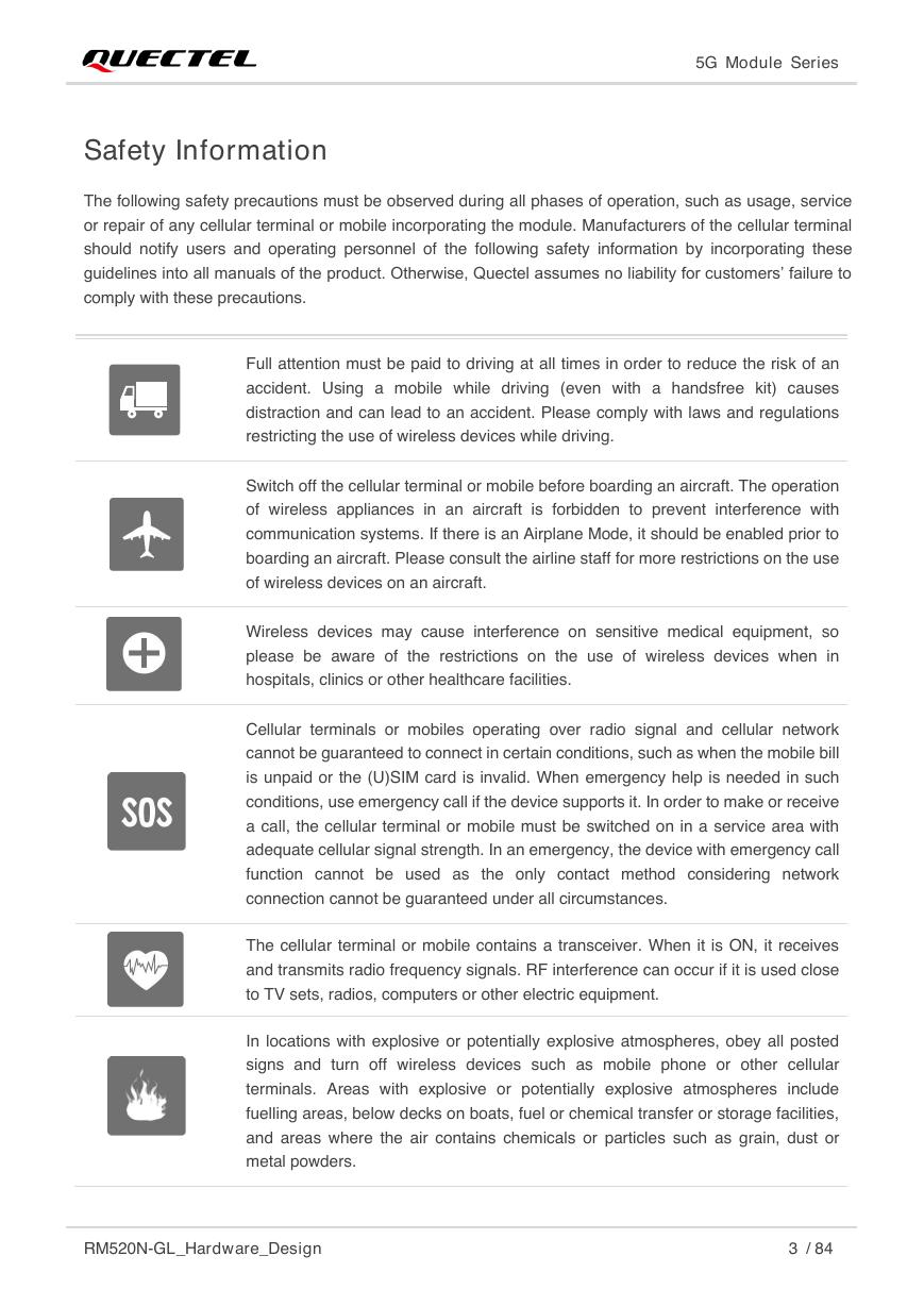
Full attention must be paid to driving at all times in order to reduce the risk of an
accident. Using a mobile while driving (even with a handsfree kit) causes
distraction and can lead to an accident. Please comply with laws and regulations
restricting the use of wireless devices while driving.
Switch off the cellular terminal or mobile before boarding an aircraft. The operation
of wireless appliances in an aircraft is forbidden to prevent interference with
communication systems. If there is an Airplane Mode, it should be enabled prior to
boarding an aircraft. Please consult the airline staff for more restrictions on the use
of wireless devices on an aircraft.
Wireless devices may cause interference on sensitive medical equipment, so
please be aware of the restrictions on the use of wireless devices when in
hospitals, clinics or other healthcare facilities.
Cellular terminals or mobiles operating over radio signal and cellular network
cannot be guaranteed to connect in certain conditions, such as when the mobile bill
is unpaid or the (U)SIM card is invalid. When emergency help is needed in such
conditions, use emergency call if the device supports it. In order to make or receive
a call, the cellular terminal or mobile must be switched on in a service area with
adequate cellular signal strength. In an emergency, the device with emergency call
function cannot be used as the only contact method considering network
connection cannot be guaranteed under all circumstances.
The cellular terminal or mobile contains a transceiver. When it is ON, it receives
and transmits radio frequency signals. RF interference can occur if it is used close
to TV sets, radios, computers or other electric equipment.
In locations with explosive or potentially explosive atmospheres, obey all posted
signs and turn off wireless devices such as mobile phone or other cellular
terminals. Areas with explosive or potentially explosive atmospheres include
fuelling areas, below decks on boats, fuel or chemical transfer or storage facilities,
and areas where the air contains chemicals or particles such as grain, dust or
metal powders.
RM520N-GL_Hardware_Design 3 / 84
�
5G Module Series
About the Document
Revision History
Version Date
Author
Description
-
2021-11-25
Wynna SHU/
Simon WANG
Juriyi XIE/
Creation of the document
1.0
2022-07-15
Wynna SHU/
First official release
Simon WANG
RM520N-GL_Hardware_Design 4 / 84
�
5G Module Series
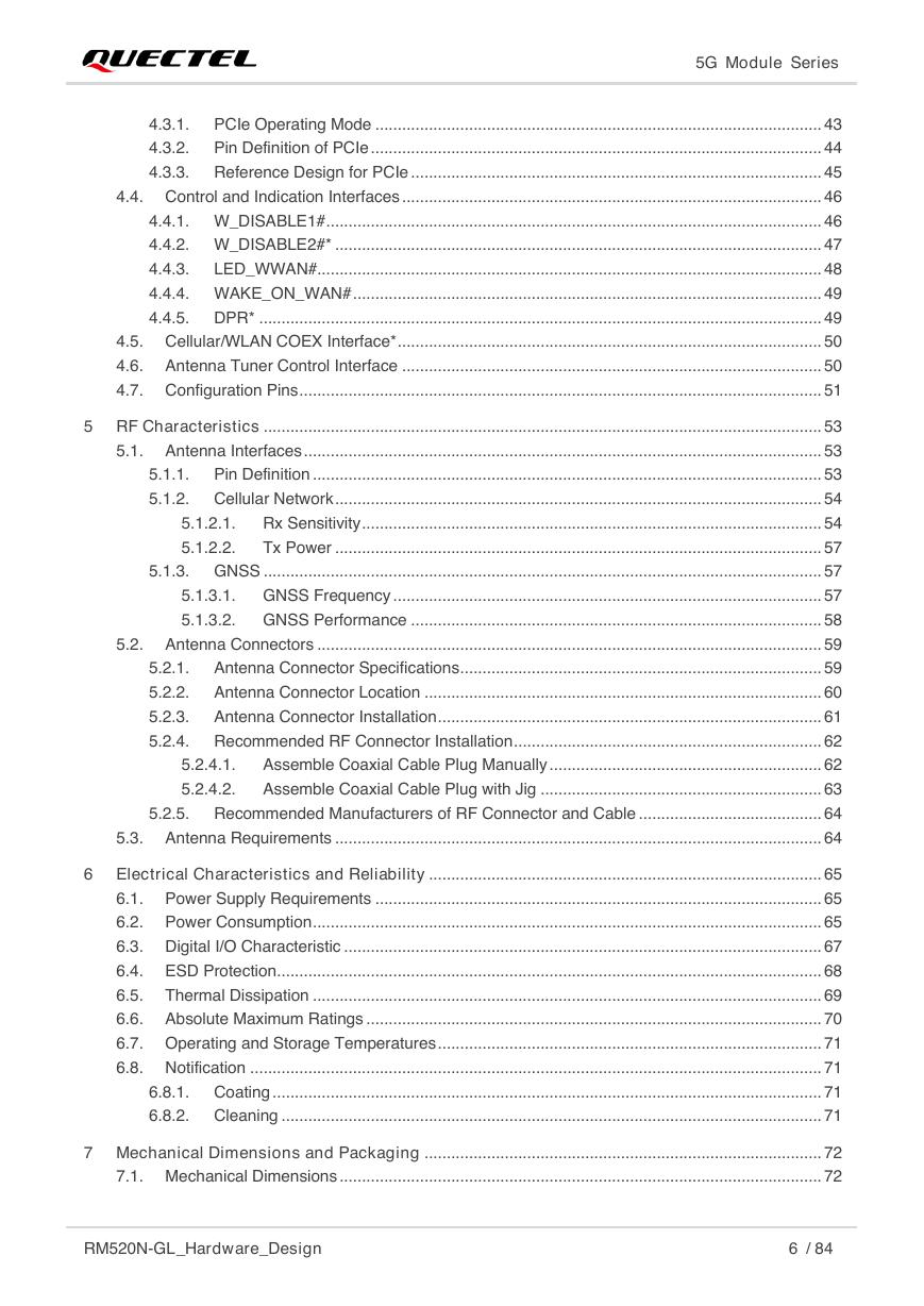
Contents
Safety Information ....................................................................................................................................... 3
About the Document ................................................................................................................................... 4
Contents ....................................................................................................................................................... 5
Table Index ................................................................................................................................................... 8
Figure Index ............................................................................................................................................... 10
1
Introduction ........................................................................................................................................ 11
1.1.
Introduction ............................................................................................................................... 11
1.2. Reference Standard .................................................................................................................. 11
1.3. Special Mark ............................................................................................................................. 12
2 Product Overview .............................................................................................................................. 13
2.1. Frequency Bands and Functions .............................................................................................. 13
2.2. Key Features ............................................................................................................................. 14
2.3. EVB Kit ...................................................................................................................................... 16
2.4. Functional Diagram ................................................................................................................... 17
2.5. Pin Assignment ......................................................................................................................... 18
2.6. Pin Description .......................................................................................................................... 19
3 Operating Characteristics ................................................................................................................. 24
3.1. Operating Modes ....................................................................................................................... 24
3.1.1. Sleep Mode .................................................................................................................... 25
3.1.2. Airplane Mode ................................................................................................................ 26
3.2. Communication Interface with a Host ....................................................................................... 26
3.3. Power Supply ............................................................................................................................ 27
3.3.1. Voltage Stability Requirements ...................................................................................... 27
3.3.2. Reference Design for Power Supply .............................................................................. 28
3.3.3. Power Supply Monitoring ............................................................................................... 29
3.4. Turn On ..................................................................................................................................... 29
3.5. Turn Off ..................................................................................................................................... 30
3.6. Reset ......................................................................................................................................... 32
4 Application Interfaces ....................................................................................................................... 36
4.1.
(U)SIM Interfaces ...................................................................................................................... 36
4.1.1. Pin Definition of (U)SIM.................................................................................................. 36
4.1.2.
(U)SIM Hot-Plug ............................................................................................................. 37
4.1.3. Normally Closed (U)SIM Card Connector...................................................................... 38
4.1.4. Normally Open (U)SIM Card Connector ........................................................................ 39
4.1.5.
(U)SIM Card Connector Without Hot-Plug ..................................................................... 39
4.1.6.
(U)SIM2 Card Compatible Design ................................................................................. 40
4.1.7.
(U)SIM Design Notices................................................................................................... 40
4.2. USB Interface ............................................................................................................................ 41
4.3. PCIe Interface ........................................................................................................................... 43
RM520N-GL_Hardware_Design 5 / 84
�
5G Module Series
4.3.1. PCIe Operating Mode .................................................................................................... 43
4.3.2. Pin Definition of PCIe ..................................................................................................... 44
4.3.3. Reference Design for PCIe ............................................................................................ 45
4.4. Control and Indication Interfaces .............................................................................................. 46
4.4.1. W_DISABLE1# ............................................................................................................... 46
4.4.2. W_DISABLE2#* ............................................................................................................. 47
4.4.3.
LED_WWAN#................................................................................................................. 48
4.4.4. WAKE_ON_WAN# ......................................................................................................... 49
4.4.5. DPR* .............................................................................................................................. 49
4.5. Cellular/WLAN COEX Interface* ............................................................................................... 50
4.6. Antenna Tuner Control Interface .............................................................................................. 50
4.7. Configuration Pins ..................................................................................................................... 51
5 RF Characteristics ............................................................................................................................. 53
5.1. Antenna Interfaces .................................................................................................................... 53
5.1.1. Pin Definition .................................................................................................................. 53
5.1.2. Cellular Network ............................................................................................................. 54
5.1.2.1. Rx Sensitivity ....................................................................................................... 54
5.1.2.2.
Tx Power ............................................................................................................. 57
5.1.3. GNSS ............................................................................................................................. 57
5.1.3.1. GNSS Frequency ................................................................................................ 57
5.1.3.2. GNSS Performance ............................................................................................ 58
5.2. Antenna Connectors ................................................................................................................. 59
5.2.1. Antenna Connector Specifications ................................................................................. 59
5.2.2. Antenna Connector Location ......................................................................................... 60
5.2.3. Antenna Connector Installation ...................................................................................... 61
5.2.4. Recommended RF Connector Installation ..................................................................... 62
5.2.4.1.
Assemble Coaxial Cable Plug Manually ............................................................. 62
5.2.4.2.
Assemble Coaxial Cable Plug with Jig ............................................................... 63
5.2.5. Recommended Manufacturers of RF Connector and Cable ......................................... 64
5.3. Antenna Requirements ............................................................................................................. 64
6 Electrical Characteristics and Reliability ........................................................................................ 65
6.1. Power Supply Requirements .................................................................................................... 65
6.2. Power Consumption .................................................................................................................. 65
6.3. Digital I/O Characteristic ........................................................................................................... 67
6.4. ESD Protection .......................................................................................................................... 68
6.5. Thermal Dissipation .................................................................................................................. 69
6.6. Absolute Maximum Ratings ...................................................................................................... 70
6.7. Operating and Storage Temperatures ...................................................................................... 71
6.8. Notification ................................................................................................................................ 71
6.8.1. Coating ........................................................................................................................... 71
6.8.2. Cleaning ......................................................................................................................... 71
7 Mechanical Dimensions and Packaging ......................................................................................... 72
7.1. Mechanical Dimensions ............................................................................................................ 72
RM520N-GL_Hardware_Design 6 / 84
�
5G Module Series
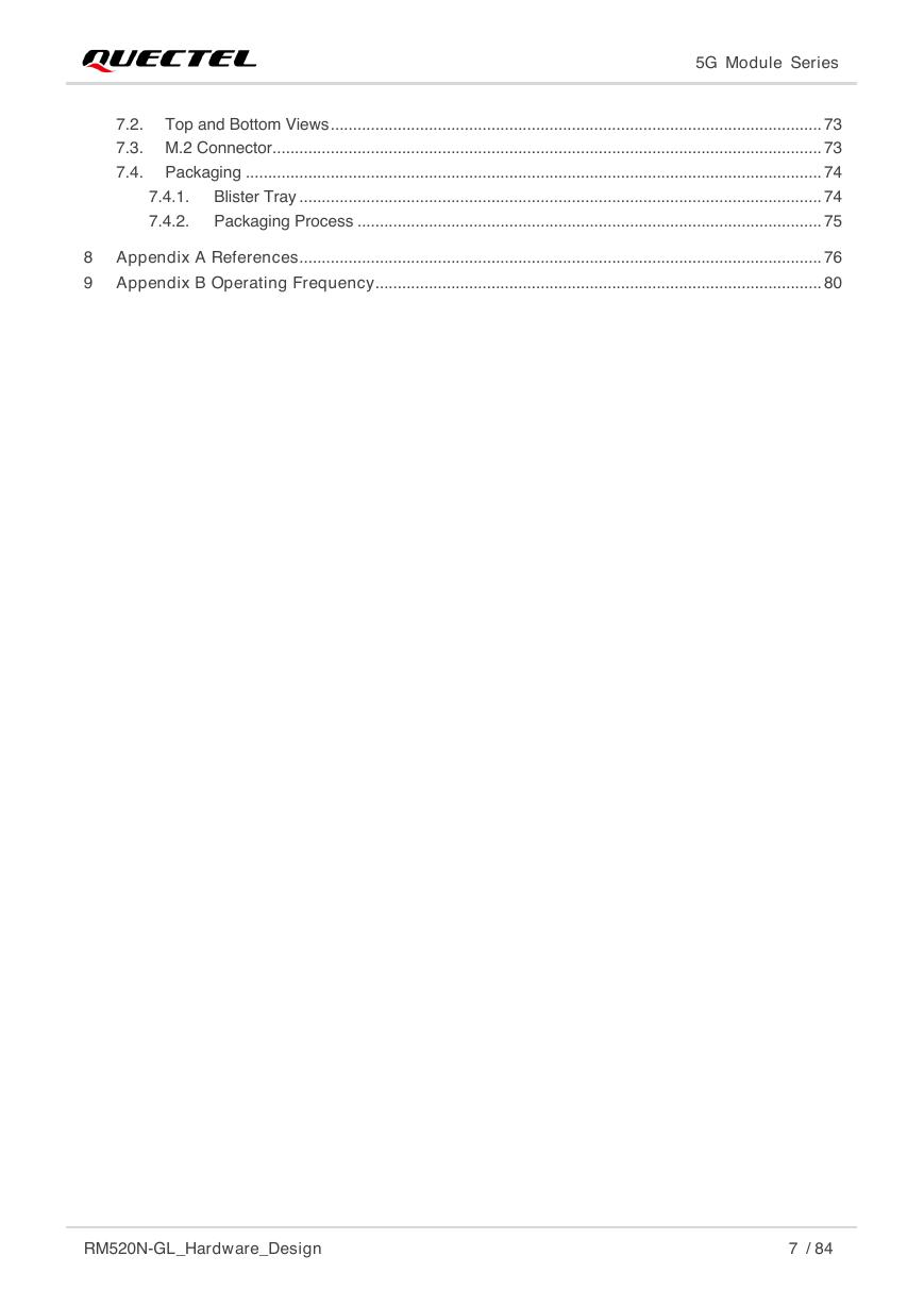
7.2. Top and Bottom Views .............................................................................................................. 73
7.3. M.2 Connector ........................................................................................................................... 73
7.4. Packaging ................................................................................................................................. 74
7.4.1. Blister Tray ..................................................................................................................... 74
7.4.2. Packaging Process ........................................................................................................ 75
8 Appendix A References ..................................................................................................................... 76
9 Appendix B Operating Frequency.................................................................................................... 80
RM520N-GL_Hardware_Design
7 / 84
�




 V2版本原理图(Capacitive-Fingerprint-Reader-Schematic_V2).pdf
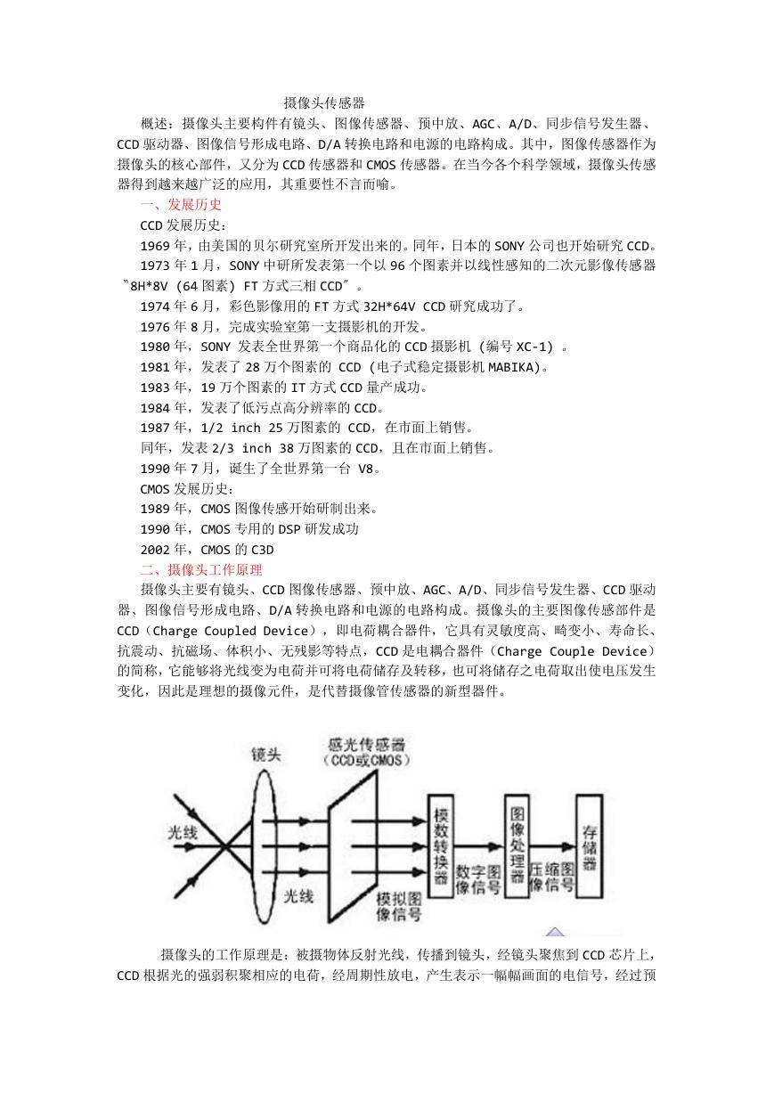 摄像头工作原理.doc
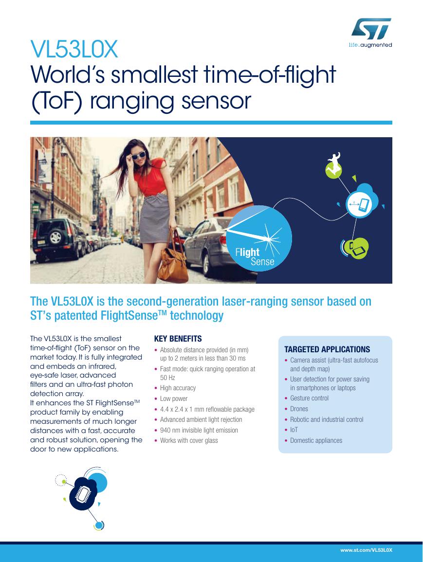 VL53L0X简要说明(En.FLVL53L00216).pdf
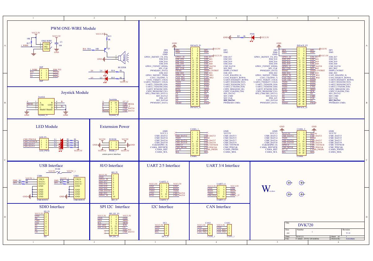 原理图(DVK720-Schematic).pdf
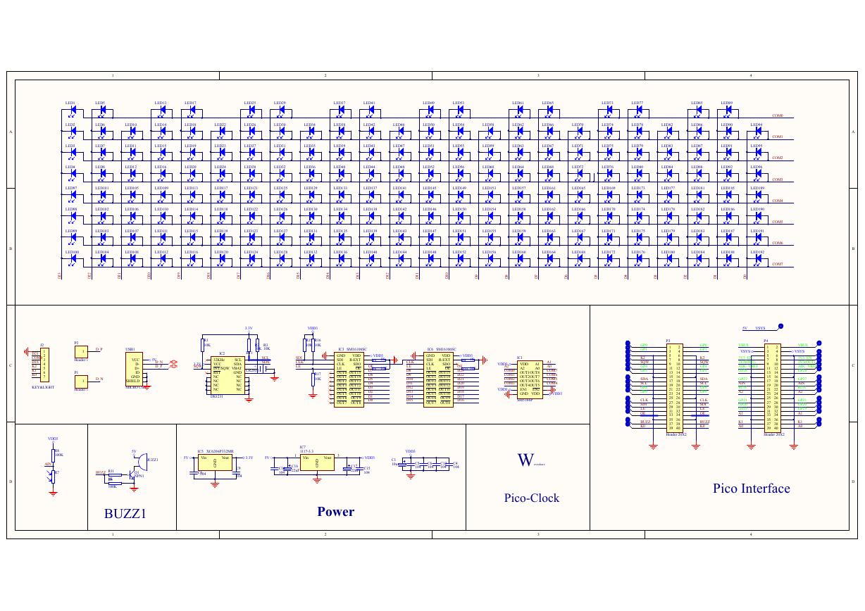 原理图(Pico-Clock-Green-Schdoc).pdf
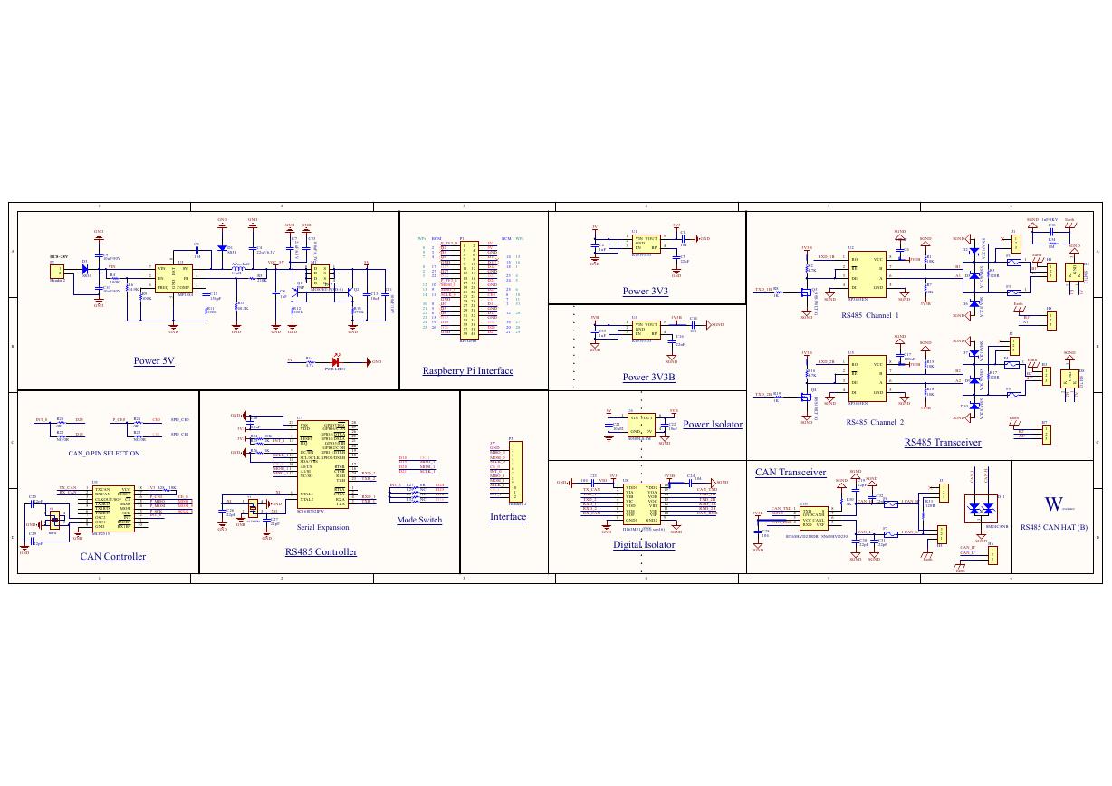 原理图(RS485-CAN-HAT-B-schematic).pdf
 File:SIM7500_SIM7600_SIM7800 Series_SSL_Application Note_V2.00.pdf
 ADS1263(Ads1262).pdf
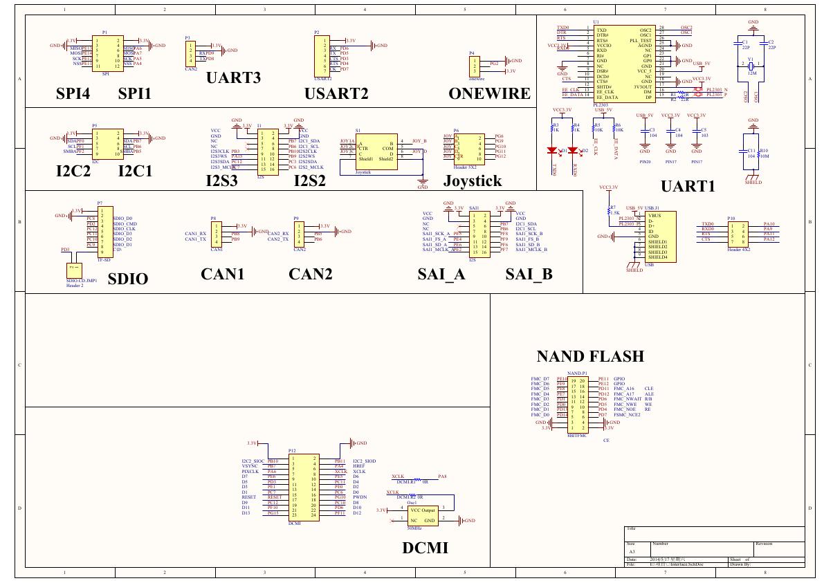 原理图(Open429Z-D-Schematic).pdf
 用户手册(Capacitive_Fingerprint_Reader_User_Manual_CN).pdf
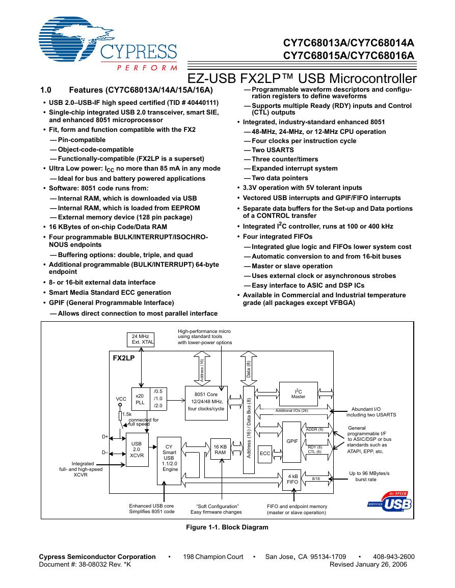 CY7C68013A(英文版)(CY7C68013A).pdf
 TechnicalReference_Dem.pdf