Description
The SP3485 device is a 3.3V low power half-duplex transceiver that
meets the specifications of the RS-485 and RS-422 serial protocols.
This device is pin-to-pin compatible with the MaxLinear SP481,
SP483 and SP485 devices as well as popular industry standards. The
SP3485 can meet the electrical specifications of the RS-485 and RS-
422 serial protocols up to 10Mbps under load.
FEATURES
■■ RS-485 and RS-422 transceiver
■■ Operates from a single 3.3V supply
■■ Interoperable with 5.0V logic
■■ Driver/receiver enable
■■ -7V to +12V common-mode input voltage
range
■■ Allows up to 32 transceivers on the serial
bus
■■ Compatibility with industry standard 75176
pinout
■■ Driver output short-circuit protection
Ordering Information - Back Page
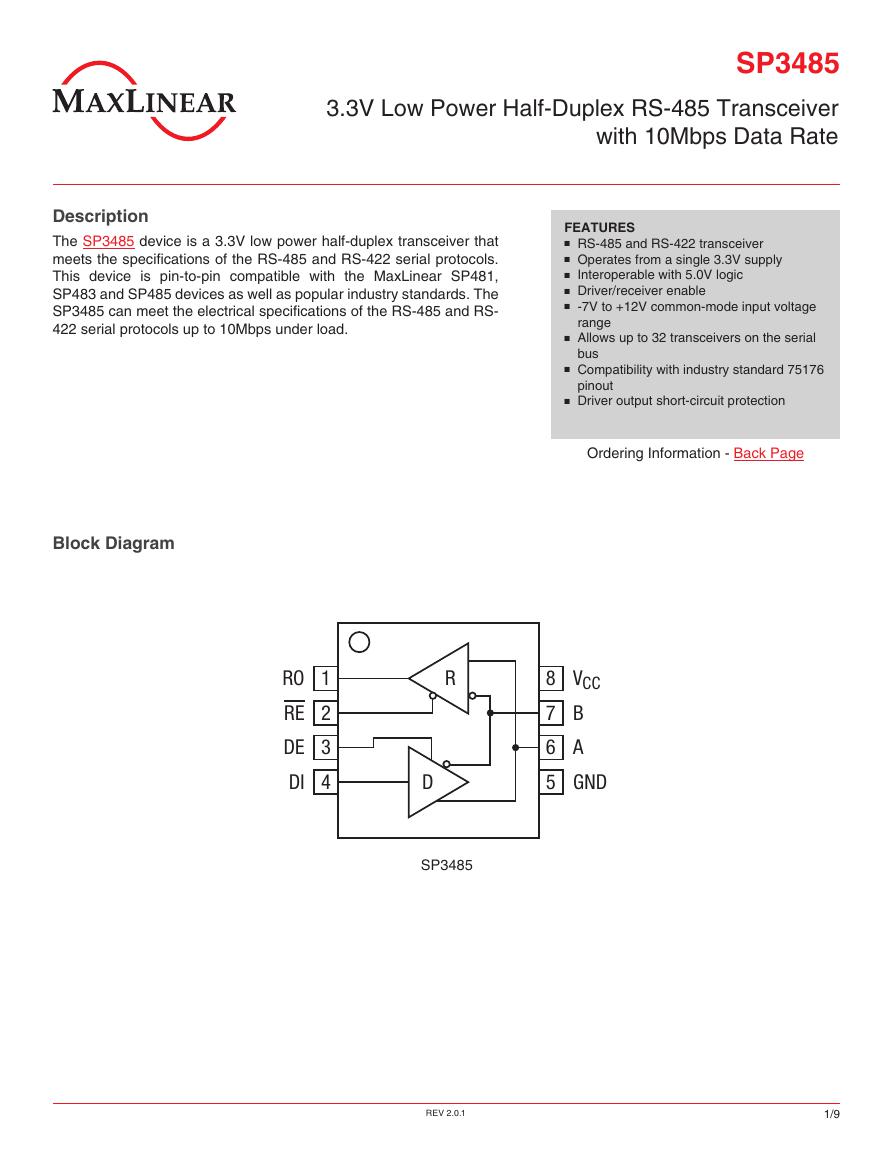
Block Diagram
RO 1
RE 2
DE 3
DI 4
R
D
SP3485
VCC
8
B7
A6
5
GND
1/9
3.3V Low Power Half-Duplex RS-485 Transceiver with 10Mbps Data RateSP3485REV 2.0.1�
Absolute Maximum Ratings
These are stress ratings only and functional operation of the
device at these ratings or any other above those indicated
in the operation sections of the specifications below is not
implied. Exposure to absolute maximum rating conditions
for extended periods of time may affect reliability.
VCC ............................................................................... 6.0V
Input Voltages
Output Voltages
Logic ..................................... -0.3V to 6.0V
Drivers .................................. -0.3V to 6.0V
Receivers ...........................................±15V
Drivers ...............................................±15V
Receivers .............................. -0.3V to 6.0V
Storage Temperature ...................................-65˚C to 150˚C
Maximum Junction Temperature, TJ ..........................125˚C
Power Dissipation .................................................... 600mW
(derate 6.90mW/°C above 70°C)
Operating Conditions
Package Power Dissipation
8-pin NSOIC ѲJA ................................................ 128.4˚C/W
ESD Rating
Human Body Model (HBM) .......................................... ±2kV
Electrical Characteristics
Unless otherwise noted: TAMB = TMIN to TMAX and VCC = 3.3V ±5%.
PARAMETERS
SP3485 Driver DC Characteristics
Differential output voltage
Differential output voltage
Differential output voltage
Change in magnitude of driver differential output
voltage for complimentary states
Driver common mode output voltage
Input high voltage
Input low voltage
Input current
Driver short circuit current VOUT = HIGH
Driver short circuit current VOUT = LOW
SP3485 Driver AC Characteristics
Maximum data rate
Driver input to output, tPLH
Driver input to output, tPHL
Differential driver skew
Driver rise or fall time
Driver enable to output high
Driver enable to output low
Driver disable time from low
Driver disable time from high
Driver enable from shutdown to output high, tPSH
Driver enable from shutdown to output low, tPSL
Time to shutdown, tSHDN
MIN.
TYP.
MAX.
UNITS
CONDITIONS
2
1.5
2.0
10
17
17
2
5
35
30
20
20
50
200
Vcc
Vcc
Vcc
0.2
3
0.8
±10
±250
±250
60
60
10
20
120
120
120
120
250
250
600
Volts
Volts
Volts
Volts
Volts
Volts
Volts
µA
mA
mA
Mbps
ns
ns
ns
ns
ns
ns
ns
ns
ns
ns
ns
Unloaded; R = ∞Ω ; Figure 1
With Load; R = 50Ω (RS-422); Figure 1
With Load; R = 27Ω (RS-485); Figure 1
R = 27Ω or R = 50Ω; Figure 1
R = 27Ω or R = 50Ω; Figure 1
Applies to DE, DI, RE
Applies to DE, DI, RE
Applies to DE, DI, RE
-7V ≤ VO ≤ +12V; Figure 8
-7V ≤ VO ≤ +12V; Figure 8
RE = VCC, DE = VCC
Figures 2 & 9
Figures 2 & 9
|tDO1- tDO2|, Figures 2 and 10
From 10%-90%; Figures 3 and 10
Figures 4 and 11
Figures 5 and 11
Figures 5 and 11
Figures 4 and 11
CL = 50pF, RL = 500Ω.
Figures 4, 5, and 11
Notes 1 and 2
2/9
SP3485REV 2.0.1�
Electrical Characteristics (Continued)
Unless otherwise noted: TAMB = TMIN to TMAX and VCC = 3.3V ±5%.
PARAMETERS
SP3485 Receiver DC Characteristics
Differential input threshold
Input hysteresis
Output voltage HIGH
Output voltage LOW
Three-state (high impedance) output current
Input resistance
Input current (A, B); VIN = 12V
Input current (A, B); VIN = -7V
Short circuit current
SP3485 Receiver AC Characteristics
Maximum data rate
Receiver input to output, tPLH
Receiver input to output, tPLH
Receiver input to output, tPHL
Receiver input to output, tPHL
Differential receiver skew
Receiver enable to output low
Receiver enable to output high
Receiver disable from low
Receiver disable from high
Receiver enable from shutdown to output high,
tPRSH
Receiver enable from shutdown to output low, tPRSL
Time to shutdown, tSHDN
Power Requirements
Supply current , no load
Supply current , no load
MIN.
TYP.
MAX.
UNITS
CONDITIONS
-0.2
Vcc-0.4
12
7
10
50
20
40
35
4
10
10
10
10
200
425
300
0.2
0.4
±1
1.0
-0.8
60
100
70
100
70
60
60
60
60
1800
1800
600
2000
1500
Volts
mV
Volts
Volts
µA
kΩ
mA
mA
mA
Mbps
ns
ns
ns
ns
ns
ns
ns
ns
ns
ns
ns
ns
µA
µA
-7V ≤ VCM ≤ 12V
VCM = 0V
VID = 200mV, -1.5mA
VID = -200mV, 2.5mA
0V ≤ VO ≤ VCC; RE = VCC
-7V ≤ VCM ≤ 12V
DE = 0V, VCC = 0V or 3.6V,
VIN = 12V
DE = 0V, VCC = 0V or 3.6V,
VIN = -7V
0V ≤ VCM ≤ VCC
RE = 0V, DE = 0V
Figures 6 and 12
TAMB = 25°C, Vcc = 3.3V,
Figures 6 and 12
Figures 6 and 12
TAMB = 25°C, Vcc = 3.3V,
Figures 6 and 12
tRSKEW = |tRPHL- tRPLH|,
Figures 6 and 12
Figures 7 and 13,
S1 closed, S2 open
Figures 7 and 13,
S2 closed, S1 open
Figures 7 and 13,
S1 closed, S2 open
Figures 7 and 13,
S2 closed, S1 open
CL = 15pF, RL = 1kΩ.
Figures 7 and 13
Notes 1 and 2
RE, DI = 0V or VCC ; DE = VCC
RE = 0V, DI = 0V or VCC, DE = 0V
NOTES:
1. The transceivers are put into shutdown by gringing RE high and DE low simultaneously for at least 600ns. If the control inputs are in this state for less than 50ns, the
device is guaranteed to not enter shutdown. If the enable inputs are held in this state for at least 600ns, the device is assured to be in shutdown. Note that the receiver
and driver times increase significantly when coming out of shutdown.
2. This spec is guaranteed by design and bench characterization.
3/9
SP3485REV 2.0.1�
Pin Functions
Pin
Name
Description
1
2
3
4
5
6
7
8
RO
RE
DE
DI
Receiver output
Receiver output enable active LOW
Driver output enable active HIGH
Driver input
GND
Ground connection
A
B
Non-inverting driver output / receiver input
Inverting driver output / receiver input
VCC
Positive supply
RO 1
RE 2
DE 3
DI 4
R
D
SP3485
Pinout (Top View)
VCC
8
B7
A6
5
GND
4/9
SP3485REV 2.0.1�
Test Circuits
D
VOD
Vcc
R
R
VOC
GENERATOR
(NOTE 1)
50Ω
D
VCC
CL
15pF
(NOTE 2)
RL
54Ω
OUT
Figure 1: Driver DC Test Load Circuit
Figure 2: Driver Propagation Delay Test Circuit
GENERATOR
(NOTE 1)
50Ω
D
VCC
CL
RL =
60Ω
OUT
C L = 15pF (NOTE 2)
S1
D
CL = 50pF
(NOTE 2)
OUT
RL = 110Ω
GENERATOR
(NOTE 1)
50Ω
Figure 3: Driver Differential Output Delay
Figure 4: Driver Enable and Disable Timing Circuit,
and Transition Time Circuit.
Output High
VCC
RL = 110Ω
OUT
0V OR 3V
D
GENERATOR
(NOTE 1)
50Ω
S1
C L = 50pF
(NOTE 2)
GENERATOR
(NOTE 1)
50Ω
VID
R
OUT
CL = 15pF
(NOTE 2)
1.5V
0V
Figure 5: Driver Enable and Disable Timing Circuit,
Figure 6: Receiver Propagation Delay Test Circuit
Output Low
1k
C L = 15pF
(NOTE 2)
S3
1.5V
-1.5V
VID
R
GENERATOR
(NOTE 1)
50Ω
S1
S2
VCC
DE = 0 or Vcc
DI = 0 or Vcc
D
A
B
IOS D
-7V to +12V V
Figure 7: Receiver Enable and Disable Timing Circuit
Figure 8: Driver Short Circuit Current Limit Test
NOTES
1: The input pulse is supplied by a generator with the following characteristics:
2: CL includes probe and stray capacitance.
PRR = 250kHz, 50% duty cycle, tR < 6.0ns, ZO = 50Ω.
5/9
SP3485REV 2.0.1�
Switching Waveforms
INPUT
Y OUTPUT
Z OUTPUT
3V
0V
VOH
VOL
VOH
VOL
1.5V
tPLH
1.5V
tPHL
VOM
VOM
tPHL
tPLH
VOM
VOM
VOM = VOH + VOL
2
≈ 1.5V
Figure 9: Driver Propagation Delay Waveforms
DE
OUTPUT
HIGH
OUTPUT
LOW
3V
0V
VOH
0V
VCC
VOL
1.5V
tPZH
tPSH
tPZL
tPSL
VOM
VOM
1.5V
tPHZ
tPLZ
0.25V
0.25V
VOM = VOH + VOL
2
≈ 1.5V
IN
1.5V
1.5V
tDO1
tDO2
90%
90%
OUT
50%
10%
tTD
50%
10%
tTD
3V
0V
2.0V
-2.0V
Figure 10: Driver Differential Output Delay
and Transition Time Waveforms
INPUT
OUTPUT
3V
0V
VCC
0V
1.5V
tRPLH
1.5V
tRPHL
VOM
VOM
VOM = VCC
2
Figure 11: Driver Enable and Disable Timing Waveforms
Figure 12: Receiver Propagation Delay Waveforms
RE
OUTPUT
3V
0V
VOH
0V
S1 is open
S2 is closed
S3 = 1.5V
1.5V
tPRHZ
10%
1.5V
tPRZH
tPRSH
S1 is closed
S2 is open
S3 = -1.5V
1.5V
tPRLZ
10%
1.5V
tPRZL
tPRSL
1.5V
3V
0V
VCC
VOL
RE
1.5V
OUTPUT
Figure 13: Receiver Enable and Disable Waveforms
6/9
SP3485REV 2.0.1�
Description
The SP3485 is a member in the family of 3.3V low power half-
duplex transceivers that meet the electrical specifications of
the RS-485 and RS-422 serial protocols. This device is pin-
to-pin compatible with the MaxLinear SP481, SP483 and
SP485 devices as well as popular industry standards. The
SP3485 feature MaxLinear’s BiCMOS process allowing low
power operationwithout sacrificing performance.
Driver
The driver outputs of the SP3485 are differential outputs
meeting the RS-485 and RS-422 standards. The typical
voltage output swing with no load will be 0 volts to 3.3 Volts.
With a load of 54Ω across the differential outputs, the drivers
can maintain greater than 1.5V voltage levels.
The driver of the SP3485 has a driver enable control line
which is active HIGH. A logic HIGH on DE (pin 3) will enable
the differential driver outputs. A logic LOW on the DE (pin
3) will tri-state the driver outputs.
The driver of the SP3485 operates up to 10Mbps. The
250mA ISC maximum limit on the driver output allows the
SP3485 to withstand an infinite short circuit over the -7.0V
to 12V common mode range without catastrophic damage
to the IC.
Receiver
The SP3485 receiver has differential inputs with an input
sensitivity of ±200mV. Input impedance of the receiver
is 12kΩ minimum. A wide common mode range of -7V to
12V allows for large ground potential differences between
systems. The receiver is equipped with a fail-safe feature
that guarantees the receiver output will be in a HIGH state
when the input is left unconnected. The receiver of the
SP3485 operates up to 10Mbps.
The receiver of the SP3485 has an enable control line
which is active LOW. A logic LOW on RE (pin 2) will enable
the differential receiver. A logic HIGH on RE (pin 2) of the
SP3485 will disable the receiver.
Low Power Shutdown Mode
Low-power shutdown mode is initiated by bringing both
RE high and DE low. In shutdown, the devices typically
draw only 50nA of supply current. RE and DE can be
driven simultaneously; the part is guaranteed not to enter
shutdown if RE is high and DE is low for less than 50ns. If
the inputs are in this state for at least 600ns, the parts are
guaranteed to enter shutdown.
Enable times tPRZH, tPZH, tPRZL and tPZL assume the part
was not in a low-power shutdown state. Enable times tPRSH,
tPSH, tPRSL and tPSL assume the parts were shut down. It
takes drivers and receivers longer to become enabled from
low-power shutdown mode (tPRSH, tPSH, tPRSL, tPSL) than
from driver/receiver-disable mode (tPRZH, tPZH, tPRZL, tPZL).
RE
X
X
0
1
RE
0
0
X
1
1
INPUTS
OUTPUTS
DE
1
1
0
0
DI
1
0
X
X
B
0
1
A
1
0
High-Z
Shutdown
Table 1: Transmit Function Truth Table
INPUTS
OUTPUTS
DE
X
X
X
1
0
VA - VB
-50mV
-200mV
Open/Shorted
RO
1
0
1
X
X
High-Z
Shutdown
Table 2: Receive Function Truth Table
7/9
SP3485REV 2.0.1�
Mechanical Dimensions
NSOIC8
Top View
Side View
Front View
Drawing No:
POD-00000108
Revision: A
8/9
SP3485REV 2.0.1�


 V2版本原理图(Capacitive-Fingerprint-Reader-Schematic_V2).pdf
 摄像头工作原理.doc
 VL53L0X简要说明(En.FLVL53L00216).pdf
 原理图(DVK720-Schematic).pdf
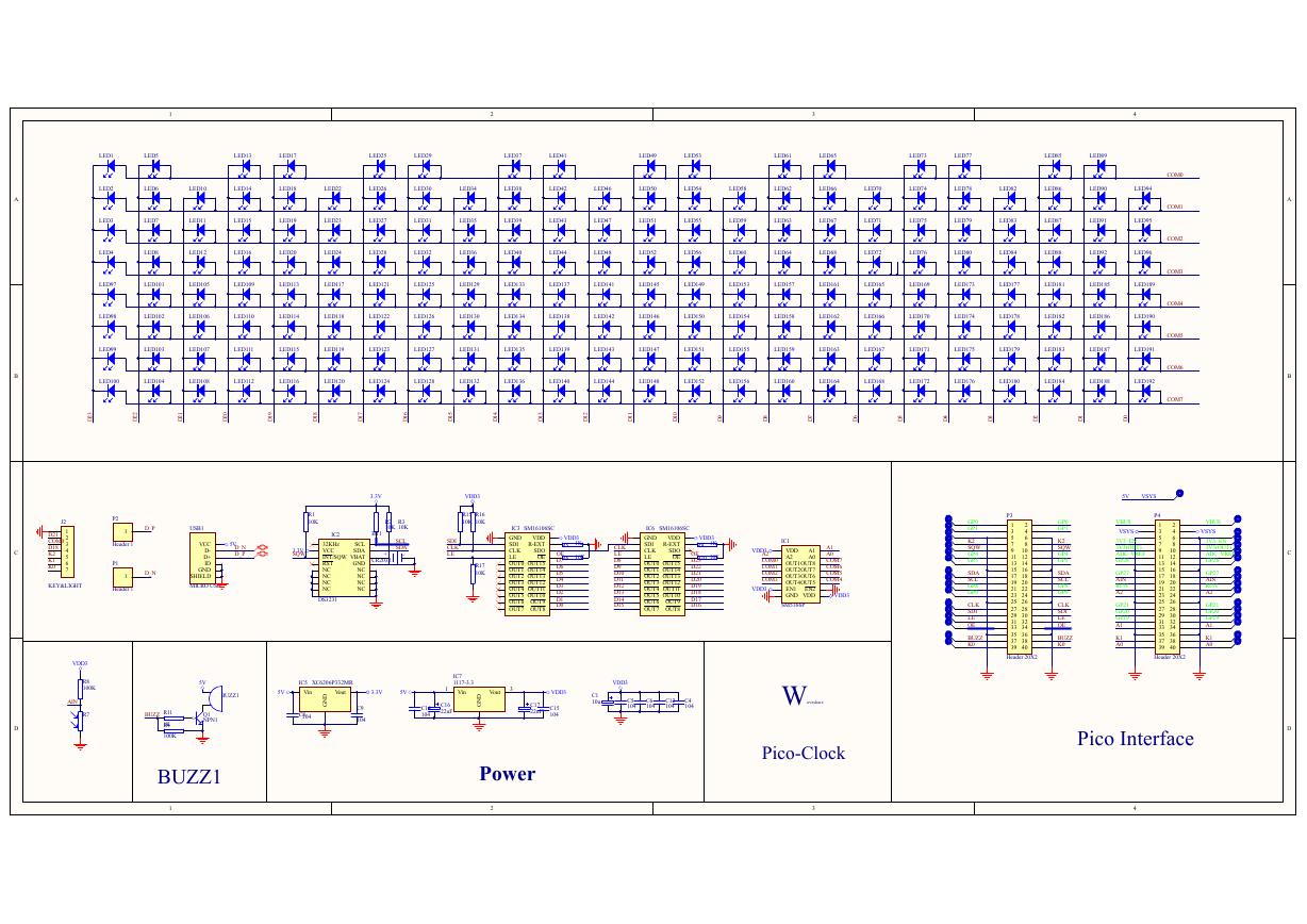 原理图(Pico-Clock-Green-Schdoc).pdf
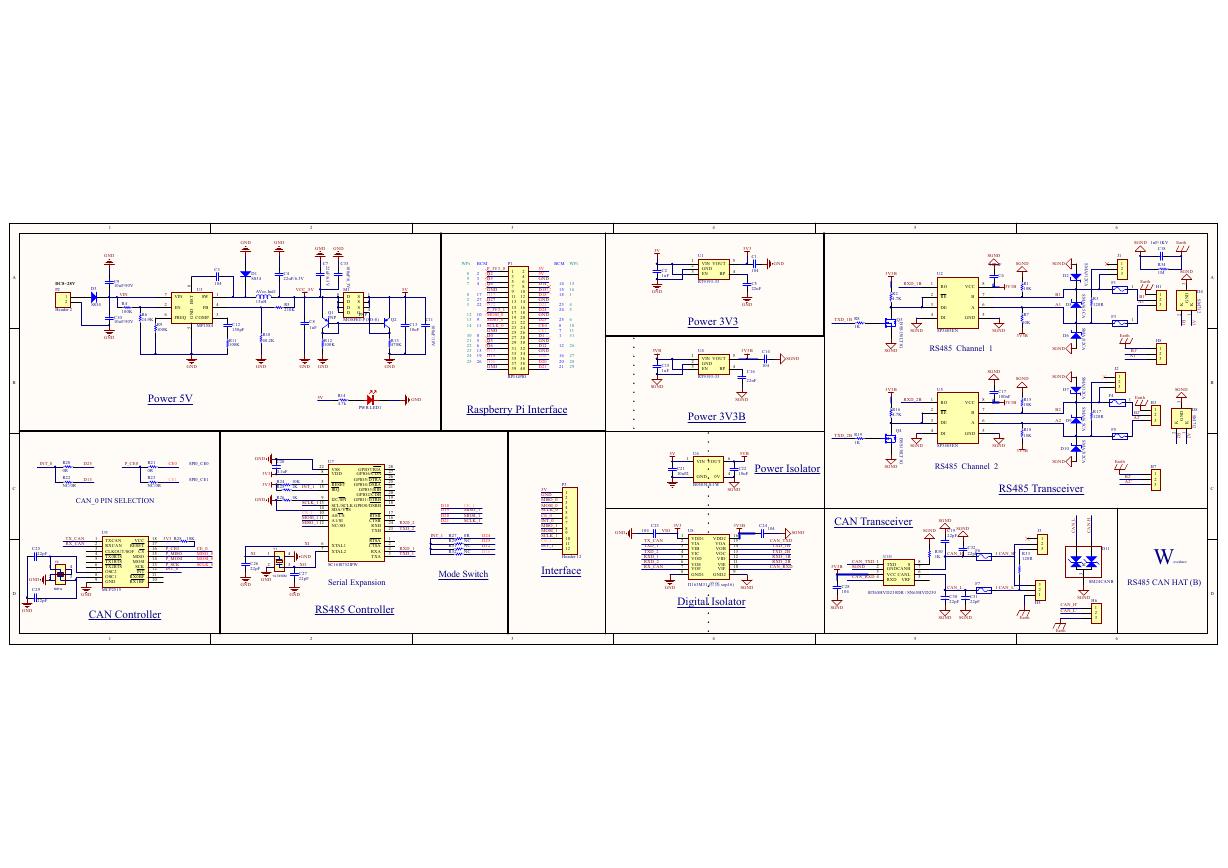 原理图(RS485-CAN-HAT-B-schematic).pdf
 File:SIM7500_SIM7600_SIM7800 Series_SSL_Application Note_V2.00.pdf
 ADS1263(Ads1262).pdf
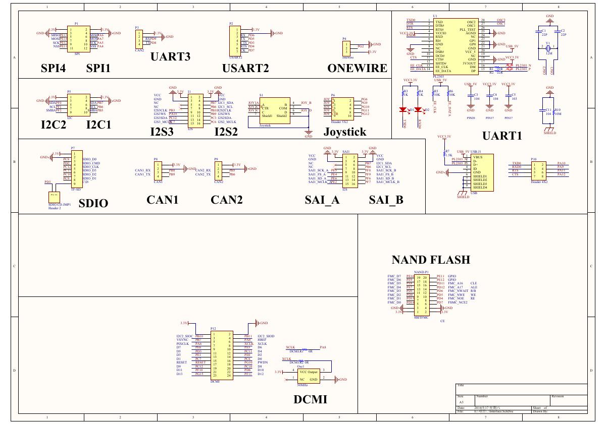 原理图(Open429Z-D-Schematic).pdf
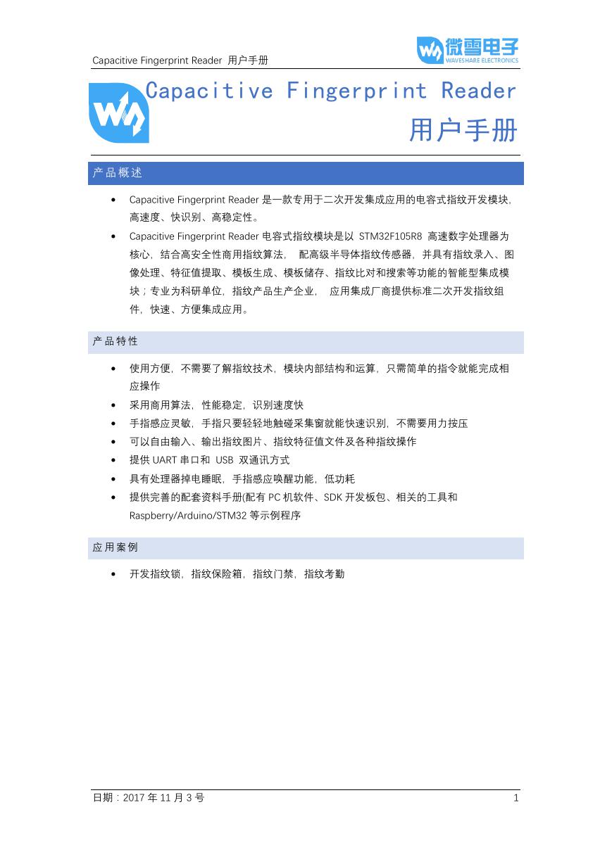 用户手册(Capacitive_Fingerprint_Reader_User_Manual_CN).pdf
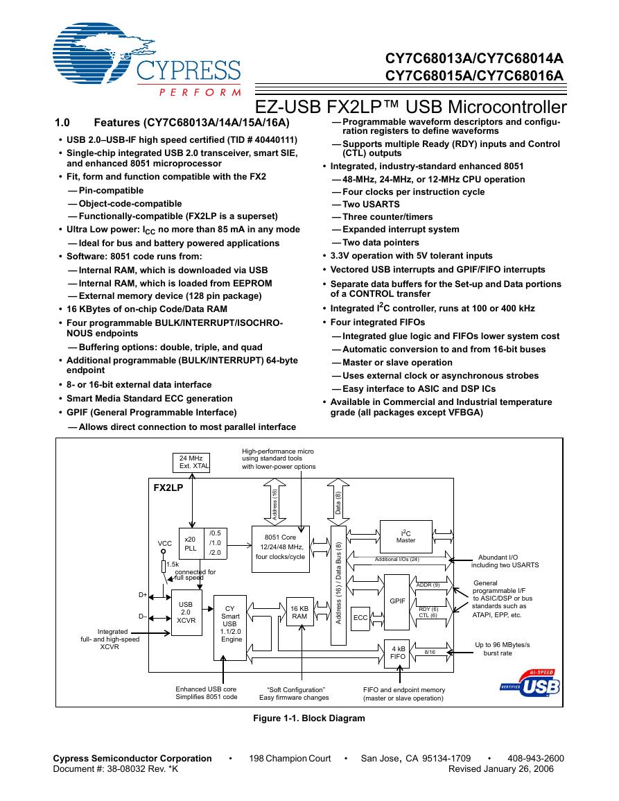 CY7C68013A(英文版)(CY7C68013A).pdf
 TechnicalReference_Dem.pdf