SNx4HC245 Octal Bus Transceivers With 3-State Outputs
SN54HC245, SN74HC245
SCLS131E –DECEMBER 1982–REVISED SEPTEMBER 2015
1 Features
1• Wide Operating Voltage Range of 2 V to 6 V
• High-Current 3-State Outputs Drive Bus Lines
Directly or Up to 15 LSTTL Loads
Low Power Consumption, 80-μA Max ICC
•
• Typical tpd = 12 ns
•
•
• On Products Compliant to MIL-PRF-38535,
±6-mA Output Drive at 5 V
Low Input Current of 1 μA Max
All Parameters Are Tested Unless Otherwise
Noted. On All Other Products, Production
Processing Does Not Necessarily Include Testing
of All Parameters.
2 Applications
• Servers
• PCs and Notebooks
• Network Switches
• Wearable Health and Fitness Devices
• Telecom Infrastructures
• Electronic Points of Sale
3 Description
These octal bus transceivers are designed for
asynchronous two-way communication between data
buses. The control-function implementation minimizes
external timing requirements.
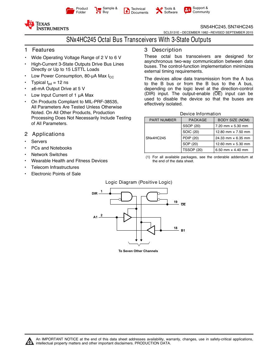
The devices allow data transmission from the A bus
to the B bus or
from the B bus to the A bus,
depending on the logic level at the direction-control
(DIR) input. The output-enable (OE) input can be
used to disable the device so that
the buses are
effectively isolated.
Device Information
PART NUMBER
PACKAGE
SNx4HC245
SSOP (20)
SOIC (20)
PDIP (20)
SOP (20)
TSSOP (20)
BODY SIZE (NOM)
7.20 mm × 5.30 mm
12.80 mm × 7.50 mm
24.33 mm × 6.35 mm
12.60 mm × 5.30 mm
6.50 mm × 4.40 mm
(1) For all available packages, see the orderable addendum at
the end of the data sheet.
Logic Diagram (Positive Logic)
1
An IMPORTANT NOTICE at the end of this data sheet addresses availability, warranty, changes, use in safety-critical applications,
intellectual property matters and other important disclaimers. PRODUCTION DATA.
DIROEA1B1121819To Seven Other ChannelsProductFolderSample &BuyTechnicalDocumentsTools &SoftwareSupport &Community�
SN54HC245, SN74HC245
SCLS131E –DECEMBER 1982–REVISED SEPTEMBER 2015
www.ti.com
Table of Contents
1
Features.................................................................. 1
2 Applications ........................................................... 1
3 Description ............................................................. 1
4 Revision History..................................................... 2
5 Pin Configuration and Functions ......................... 3
6 Specifications......................................................... 4
6.1 Absolute Maximum Ratings ...................................... 4
6.2 ESD Ratings.............................................................. 4
6.3 Recommended Operating Conditions....................... 4
6.4 Thermal Information.................................................. 5
6.5 Electrical Characteristics........................................... 5
6.6 Switching Characteristics, CL = 50 pF ...................... 5
6.7 Switching Characteristics, CL = 150 pF .................... 6
6.8 Operating Characteristics.......................................... 6
6.9 Typical Characteristics.............................................. 6
7 Parameter Measurement Information .................. 7
8 Detailed Description .............................................. 8
8.1 Overview ................................................................... 8
8.2 Functional Block Diagram ......................................... 8
8.3 Feature Description................................................... 8
8.4 Device Functional Modes.......................................... 8
9 Application and Implementation .......................... 9
9.1 Application Information.............................................. 9
9.2 Typical Application ................................................... 9
10 Power Supply Recommendations ..................... 10
11 Layout................................................................... 10
11.1 Layout Guidelines ................................................. 10
11.2 Layout Example .................................................... 10
12 Device and Documentation Support ................. 11
12.1 Related Links ........................................................ 11
12.2 Community Resources.......................................... 11
12.3 Trademarks ........................................................... 11
12.4 Electrostatic Discharge Caution............................ 11
12.5 Glossary ................................................................ 11
13 Mechanical, Packaging, and Orderable
Information ........................................................... 11
4 Revision History
NOTE: Page numbers for previous revisions may differ from page numbers in the current version.
Changes from Revision D (August 2003) to Revision E
Page
• Added Device Comparison section, Thermal Informationsection , ESD Ratings section, Application and
Implementation section, Power Supply Recommendations section, and Layout section. ..................................................... 1
• Added Military Disclaimer to Features list. ............................................................................................................................. 1
• Updated FK package pinout drawing. .................................................................................................................................... 3
2
Submit Documentation Feedback
Copyright © 1982–2015, Texas Instruments Incorporated
Product Folder Links: SN54HC245 SN74HC245
�
www.ti.com
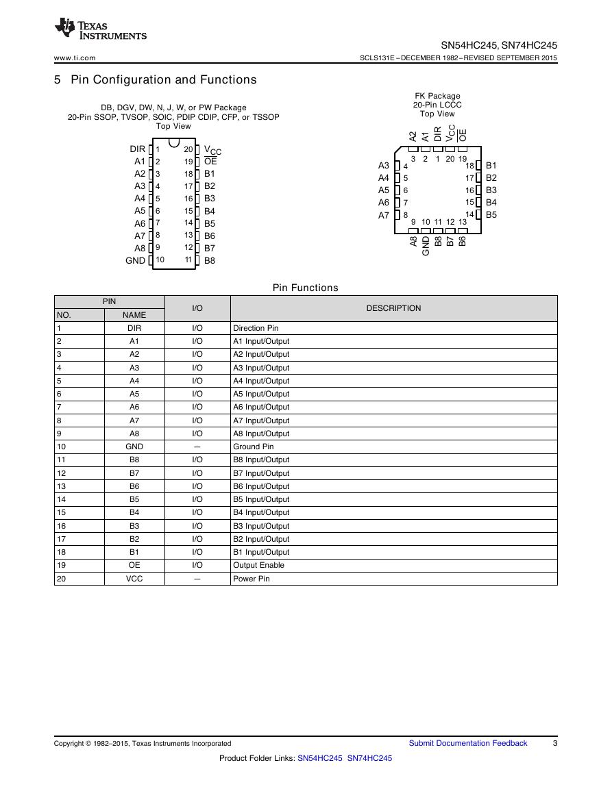
5 Pin Configuration and Functions
DB, DGV, DW, N, J, W, or PW Package
20-Pin SSOP, TVSOP, SOIC, PDIP CDIP, CFP, or TSSOP
Top View
SN54HC245, SN74HC245
SCLS131E –DECEMBER 1982–REVISED SEPTEMBER 2015
FK Package
20-Pin LCCC
Top View
NO.
1
2
3
4
5
6
7
8
9
10
11
12
13
14
15
16
17
18
19
20
PIN
NAME
DIR
A1
A2
A3
A4
A5
A6
A7
A8
GND
B8
B7
B6
B5
B4
B3
B2
B1
OE
VCC
I/O
I/O
I/O
I/O
I/O
I/O
I/O
I/O
I/O
I/O
—
I/O
I/O
I/O
I/O
I/O
I/O
I/O
I/O
I/O
—
Pin Functions
DESCRIPTION
Direction Pin
A1 Input/Output
A2 Input/Output
A3 Input/Output
A4 Input/Output
A5 Input/Output
A6 Input/Output
A7 Input/Output
A8 Input/Output
Ground Pin
B8 Input/Output
B7 Input/Output
B6 Input/Output
B5 Input/Output
B4 Input/Output
B3 Input/Output
B2 Input/Output
B1 Input/Output
Output Enable
Power Pin
Copyright © 1982–2015, Texas Instruments Incorporated
Submit Documentation Feedback
3
Product Folder Links: SN54HC245 SN74HC245
1234567891020191817161514131211DIRA1A2A3A4A5A6A7A8GNDVCCOEB1B2B3B4B5B6B7B83212019910111213456781817161514B1B2B3B4B5A3A4A5A6A7A2A1DIRB7B6OEA8GNDB8VCC�
SN54HC245, SN74HC245
SCLS131E –DECEMBER 1982–REVISED SEPTEMBER 2015
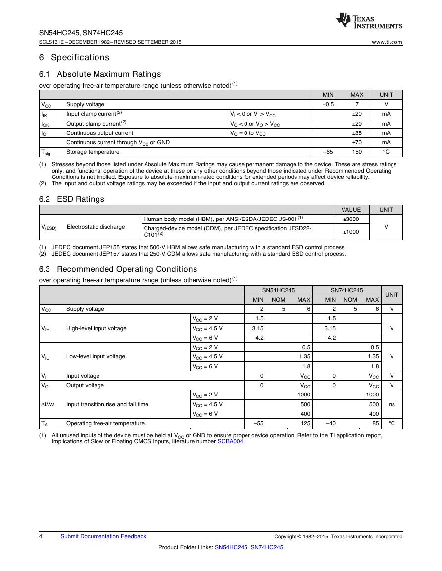
6 Specifications
6.1 Absolute Maximum Ratings
over operating free-air temperature range (unless otherwise noted)(1)
VCC
IIK
IOK
IO
Supply voltage
Input clamp current(2)
Output clamp current(2)
Continuous output current
Continuous current through VCC or GND
Storage temperature
MIN
−0.5
VI < 0 or VI > VCC
VO < 0 or VO > VCC
VO = 0 to VCC
www.ti.com
MAX
UNIT
7
±20
±20
±35
±70
150
V
mA
mA
mA
mA
°C
Tstg
(1) Stresses beyond those listed under Absolute Maximum Ratings may cause permanent damage to the device. These are stress ratings
only, and functional operation of the device at these or any other conditions beyond those indicated under Recommended Operating
Conditions is not implied. Exposure to absolute-maximum-rated conditions for extended periods may affect device reliability.
–65
(2) The input and output voltage ratings may be exceeded if the input and output current ratings are observed.
6.2 ESD Ratings
V(ESD)
Electrostatic discharge
Human body model (HBM), per ANSI/ESDA/JEDEC JS-001(1)
Charged-device model (CDM), per JEDEC specification JESD22-
C101(2)
VALUE
±3000
±1000
UNIT
V
(1)
(2)
JEDEC document JEP155 states that 500-V HBM allows safe manufacturing with a standard ESD control process.
JEDEC document JEP157 states that 250-V CDM allows safe manufacturing with a standard ESD control process.
6.3 Recommended Operating Conditions
over operating free-air temperature range (unless otherwise noted)(1)
SN54HC245
SN74HC245
VCC
VIH
VIL
VI
VO
Supply voltage
High-level input voltage
Low-level input voltage
Input voltage
Output voltage
∆t/∆v
Input transition rise and fall time
VCC = 2 V
VCC = 4.5 V
VCC = 6 V
VCC = 2 V
VCC = 4.5 V
VCC = 6 V
VCC = 2 V
VCC = 4.5 V
VCC = 6 V
MAX
6
MIN NOM
5
2
1.5
3.15
4.2
MIN NOM MAX
6
5
2
1.5
3.15
4.2
0
0
0
0
0.5
1.35
1.8
VCC
VCC
1000
500
400
125
UNIT
V
V
V
V
V
ns
°C
0.5
1.35
1.8
VCC
VCC
1000
500
400
85
Operating free-air temperature
TA
(1) All unused inputs of the device must be held at VCC or GND to ensure proper device operation. Refer to the TI application report,
–55
–40
Implications of Slow or Floating CMOS Inputs, literature number SCBA004.
4
Submit Documentation Feedback
Copyright © 1982–2015, Texas Instruments Incorporated
Product Folder Links: SN54HC245 SN74HC245
�
www.ti.com
6.4 Thermal Information
THERMAL METRIC(1)
DB
(SSOP)
DW
(SOIC)
SN54HC245, SN74HC245
SCLS131E –DECEMBER 1982–REVISED SEPTEMBER 2015
SNx4HC245
N
(PDIP)
20 PINS
NS
(SOP)
PW
(TSSOP)
UNIT
Junction-to-ambient thermal resistance
Junction-to-case (top) thermal resistance
Junction-to-board thermal resistance
Junction-to-top characterization parameter
Junction-to-board characterization parameter
RθJA
RθJC(top)
RθJB
ψJT
ψJB
(1) For more information about traditional and new thermal metrics, see the Semiconductor and IC Package Thermal Metrics application
92.1
53.9
47.2
16.5
46.8
77.0
41.5
44.8
16.8
44.3
57.0
48.6
38.0
25.4
37.8
74.1
40.6
41.6
14.8
41.2
99.7
34.0
50.7
1.8
50.1
°C/W
°C/W
°C/W
°C/W
°C/W
report, SPRA953.
6.5 Electrical Characteristics
over recommended operating free-air temperature range (unless otherwise noted)
PARAMETER
TEST CONDITIONS
VOH
VI = VIH or VIL
VOL
II
IOZ
ICC
Ci
VI = VIH or VIL
DIR or OE VI = VCC or 0
VO = VCC or 0
A or B
VI = VCC or 0,
DIR or OE
IO = 0
IOH = –20 µA
IOH = –6 mA
IOH = –7.8 mA
IOL = 20 µA
IOL = 6 mA
IOL = 7.8 mA
MIN
1.9
4.4
5.9
3.98
5.48
VCC
2 V
4.5 V
6 V
4.5 V
6 V
2 V
4.5 V
6 V
4.5 V
6 V
6 V
6 V
6 V
TA = 25°C
TYP MAX
1.998
4.499
5.999
4.3
5.8
0.002
0.001
0.001
0.17
0.15
±0.1
±0.01
0.1
0.1
0.1
0.26
0.26
±100
±0.5
8
10
2 V to 6 V
3
MAX
SN54HC245
MIN
1.9
4.4
5.9
3.7
5.2
MAX
SN74HC245
MIN
1.9
4.4
5.9
3.84
5.34
0.1
0.1
0.1
0.4
0.4
±1000
±10
160
10
0.1
0.1
0.1
0.33
0.33
±1000
±5
80
10
6.6 Switching Characteristics, CL = 50 pF
over recommended operating free-air temperature range (unless otherwise noted)
(see Figure 3)
PARAMETER
FROM
(INPUT)
TO
(OUTPUT)
tpd
ten
tdis
tt
A or B
B or A
OE
A or B
OE
A or B
A or B
VCC
2 V
4.5 V
6 V
2 V
4.5 V
6 V
2 V
4.5 V
6 V
2 V
4.5 V
6 V
MIN
TA = 25°C
TYP
40
15
12
125
23
20
74
25
21
20
8
6
MAX
105
21
18
230
46
39
200
40
34
60
12
10
SN54HC245
MIN
MAX
160
32
27
340
68
58
300
60
51
90
18
15
SN74HC245
MIN
MAX
130
26
22
290
58
49
250
50
43
75
15
13
UNIT
V
V
nA
µA
µA
pF
UNIT
ns
ns
ns
ns
Copyright © 1982–2015, Texas Instruments Incorporated
Submit Documentation Feedback
5
Product Folder Links: SN54HC245 SN74HC245
�
SN54HC245, SN74HC245
SCLS131E –DECEMBER 1982–REVISED SEPTEMBER 2015
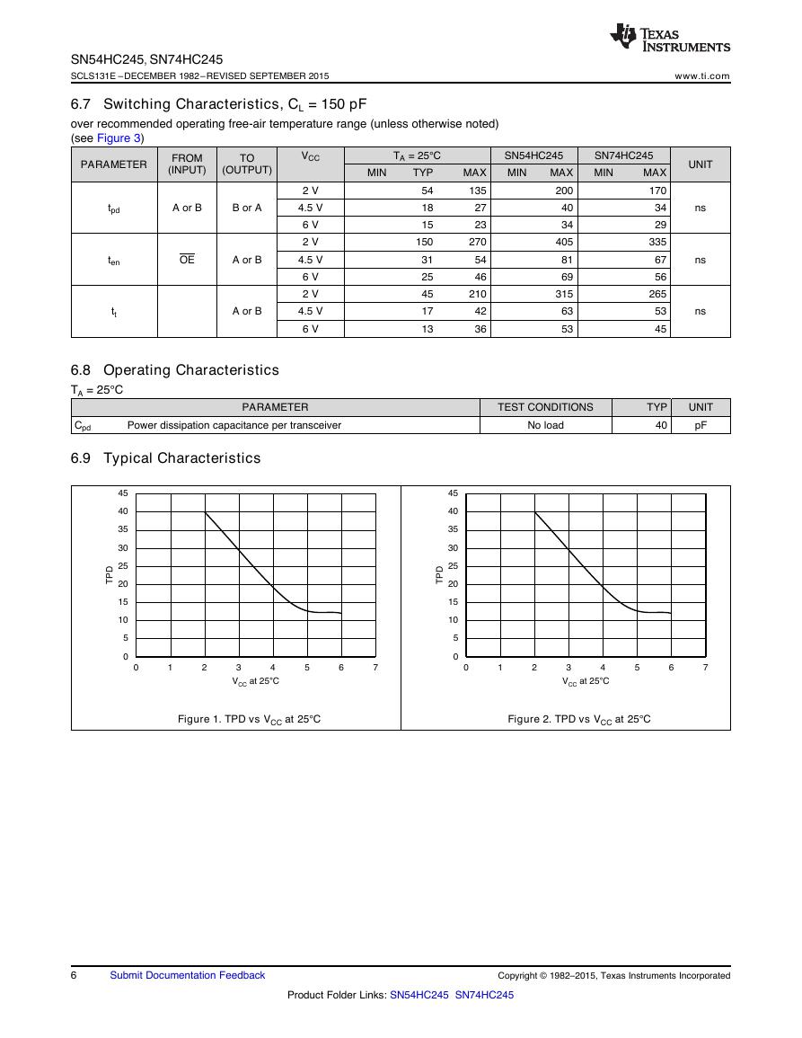
6.7 Switching Characteristics, CL = 150 pF
over recommended operating free-air temperature range (unless otherwise noted)
(see Figure 3)
www.ti.com
PARAMETER
FROM
(INPUT)
TO
(OUTPUT)
tpd
ten
tt
A or B
B or A
OE
A or B
A or B
VCC
2 V
4.5 V
6 V
2 V
4.5 V
6 V
2 V
4.5 V
6 V
MIN
TA = 25°C
TYP
54
18
15
150
31
25
45
17
13
MAX
135
27
23
270
54
46
210
42
36
SN54HC245
MIN
MAX
200
40
34
405
81
69
315
63
53
SN74HC245
MIN
MAX
170
34
29
335
67
56
265
53
45
UNIT
ns
ns
ns
6.8 Operating Characteristics
TA = 25°C
Cpd
Power dissipation capacitance per transceiver
PARAMETER
6.9 Typical Characteristics
TEST CONDITIONS
No load
TYP
40
UNIT
pF
Figure 1. TPD vs VCC at 25°C
Figure 2. TPD vs VCC at 25°C
6
Submit Documentation Feedback
Copyright © 1982–2015, Texas Instruments Incorporated
Product Folder Links: SN54HC245 SN74HC245
05101520253035404501234567TPD VCC at 25SC C002 05101520253035404501234567TPD VCC at 25SC C002 �
www.ti.com
7 Parameter Measurement Information
SN54HC245, SN74HC245
SCLS131E –DECEMBER 1982–REVISED SEPTEMBER 2015
A. CL includes probe and test-fixture capacitance.
B. Waveform 1 is for an output with internal conditions such that the output is low except when disabled by the output
control.
Waveform 2 is for an output with internal conditions such that the output is high except when disabled by the output
control.
C. Phase relationships between waveforms were chosen arbitrarily. All input pulses are supplied by generators having
the following characteristics: PRR ≤ 1 MHz, ZO = 50 Ω, tr = 6 ns, tf = 6 ns.
The outputs are measured one at a time with one input transition per measurement.
tPLZ and tPHZ are the same as tdis.
tPZL and tPZH are the same as ten.
tPLH and tPHL are the same as tpd.
D.
E.
F.
G.
Figure 3. Load Circuit and Voltage Waveforms
Copyright © 1982–2015, Texas Instruments Incorporated
Submit Documentation Feedback
7
Product Folder Links: SN54HC245 SN74HC245
VOLTAGEWAVEFORMINPUTRISEANDFALLTIMES50%50%10%10%90%90%VCC0 VtrtInputfVOLTAGEWAVEFORMSPROPAGATION DELAYAND OUTPUT TRANSITION TIMES50%50%50%10%10%90%90%VCCVOHVOL0 VtrtInputfIn-PhaseOutput50%tPLHtPHL50%50%10%10%90%90%VOHVOLttrftPHLtPLHOut-of-PhaseOutput50%10%90%VCC≈VCCVOL0 VOutputControl(Low-LevelEnabling)OutputWaveform1(See Note B)50%tPZLtPLZVOLTAGEWAVEFORMSENABLEANDDISABLETIMESFOR3-STATEOUTPUTSVOH≈0 V50%50%tPZHtPHZOutputWaveform 2(See Note B)≈VCCTestPointFrom OutputUnderTestCL(see NoteA)RLVCCS1S2LOAD CIRCUITPARAMETERCLtPZHtpdor tttdistentPZLtPHZtPLZ1 kΩ1 kΩ50 pFor150 pF50 pFOpenClosedRS1LClosedOpenS2OpenClosedClosedOpen50 pFor150 pFOpenOpen−−�
SN54HC245, SN74HC245
SCLS131E –DECEMBER 1982–REVISED SEPTEMBER 2015
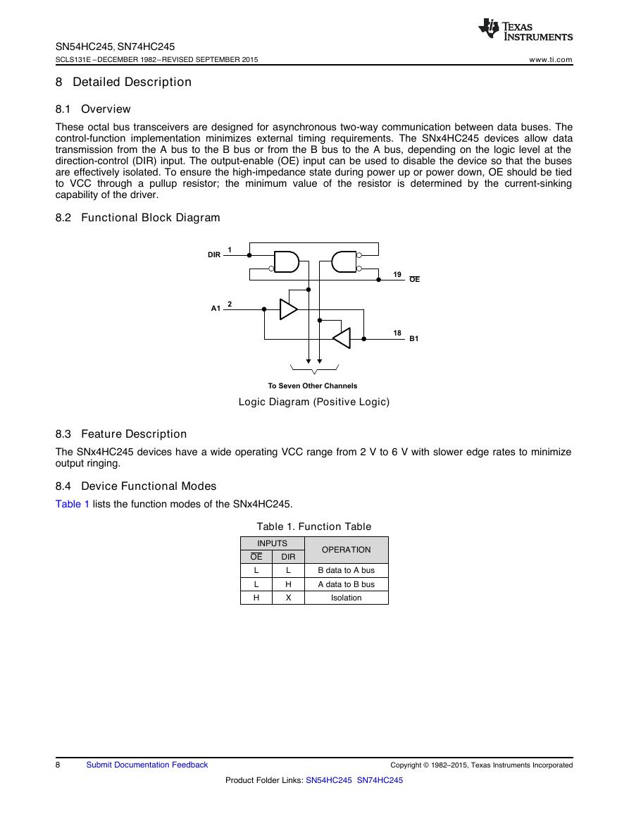
8 Detailed Description
www.ti.com
8.1 Overview
These octal bus transceivers are designed for asynchronous two-way communication between data buses. The
control-function implementation minimizes external timing requirements. The SNx4HC245 devices allow data
transmission from the A bus to the B bus or from the B bus to the A bus, depending on the logic level at the
direction-control (DIR) input. The output-enable (OE) input can be used to disable the device so that the buses
are effectively isolated. To ensure the high-impedance state during power up or power down, OE should be tied
to VCC through a pullup resistor;
the resistor is determined by the current-sinking
capability of the driver.
the minimum value of
8.2 Functional Block Diagram
Logic Diagram (Positive Logic)
8.3 Feature Description
The SNx4HC245 devices have a wide operating VCC range from 2 V to 6 V with slower edge rates to minimize
output ringing.
8.4 Device Functional Modes
Table 1 lists the function modes of the SNx4HC245.
Table 1. Function Table
INPUTS
OPERATION
OE
L
L
H
DIR
L
H
X
B data to A bus
A data to B bus
Isolation
8
Submit Documentation Feedback
Copyright © 1982–2015, Texas Instruments Incorporated
Product Folder Links: SN54HC245 SN74HC245
DIROEA1B1121819To Seven Other Channels�




 V2版本原理图(Capacitive-Fingerprint-Reader-Schematic_V2).pdf
 摄像头工作原理.doc
 VL53L0X简要说明(En.FLVL53L00216).pdf
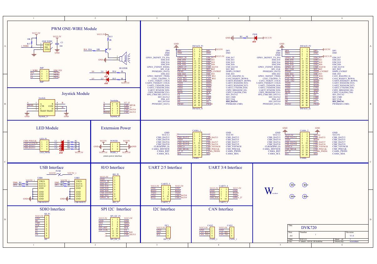 原理图(DVK720-Schematic).pdf
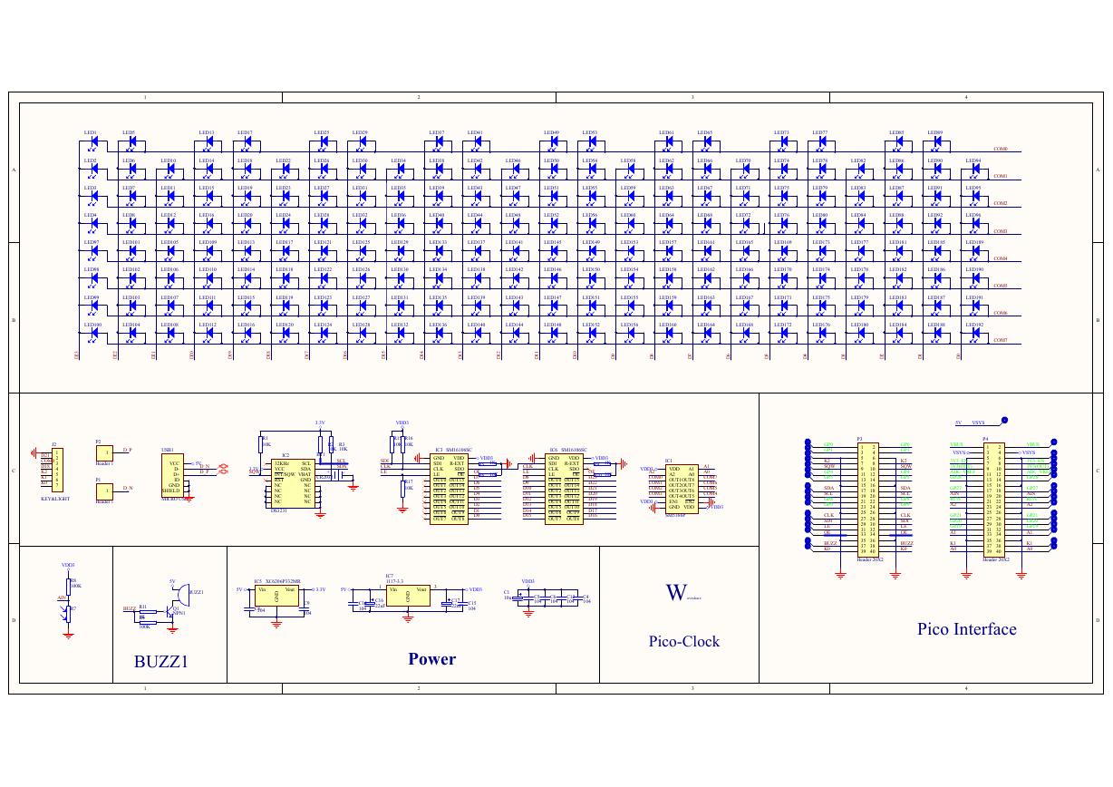 原理图(Pico-Clock-Green-Schdoc).pdf
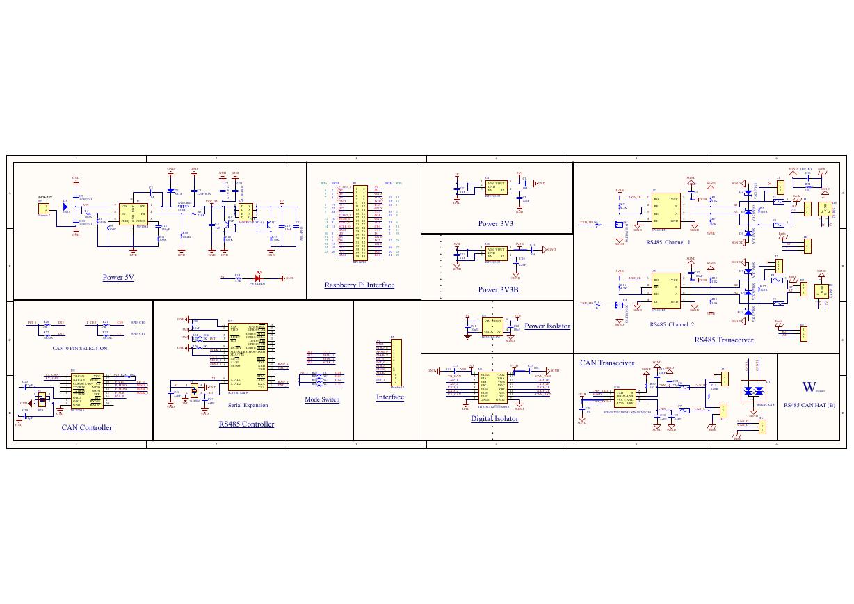 原理图(RS485-CAN-HAT-B-schematic).pdf
 File:SIM7500_SIM7600_SIM7800 Series_SSL_Application Note_V2.00.pdf
 ADS1263(Ads1262).pdf
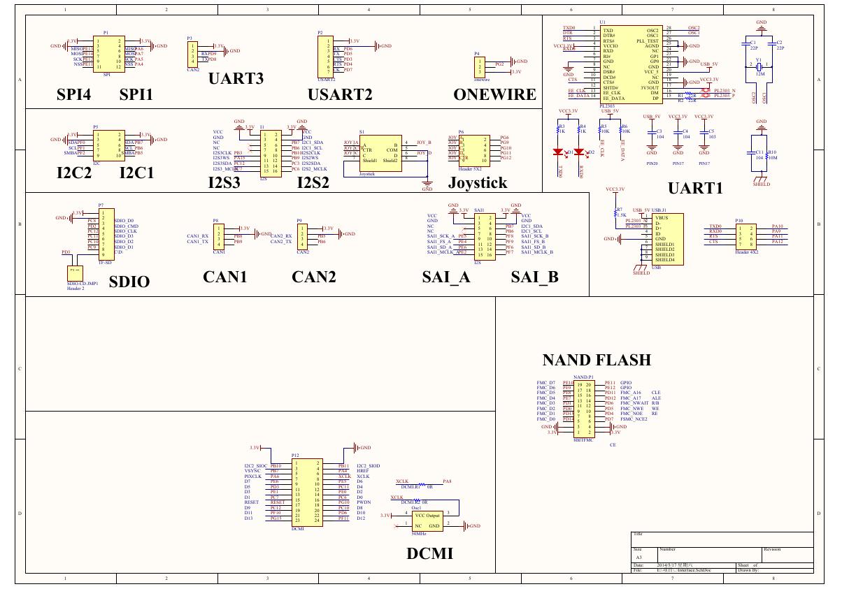 原理图(Open429Z-D-Schematic).pdf
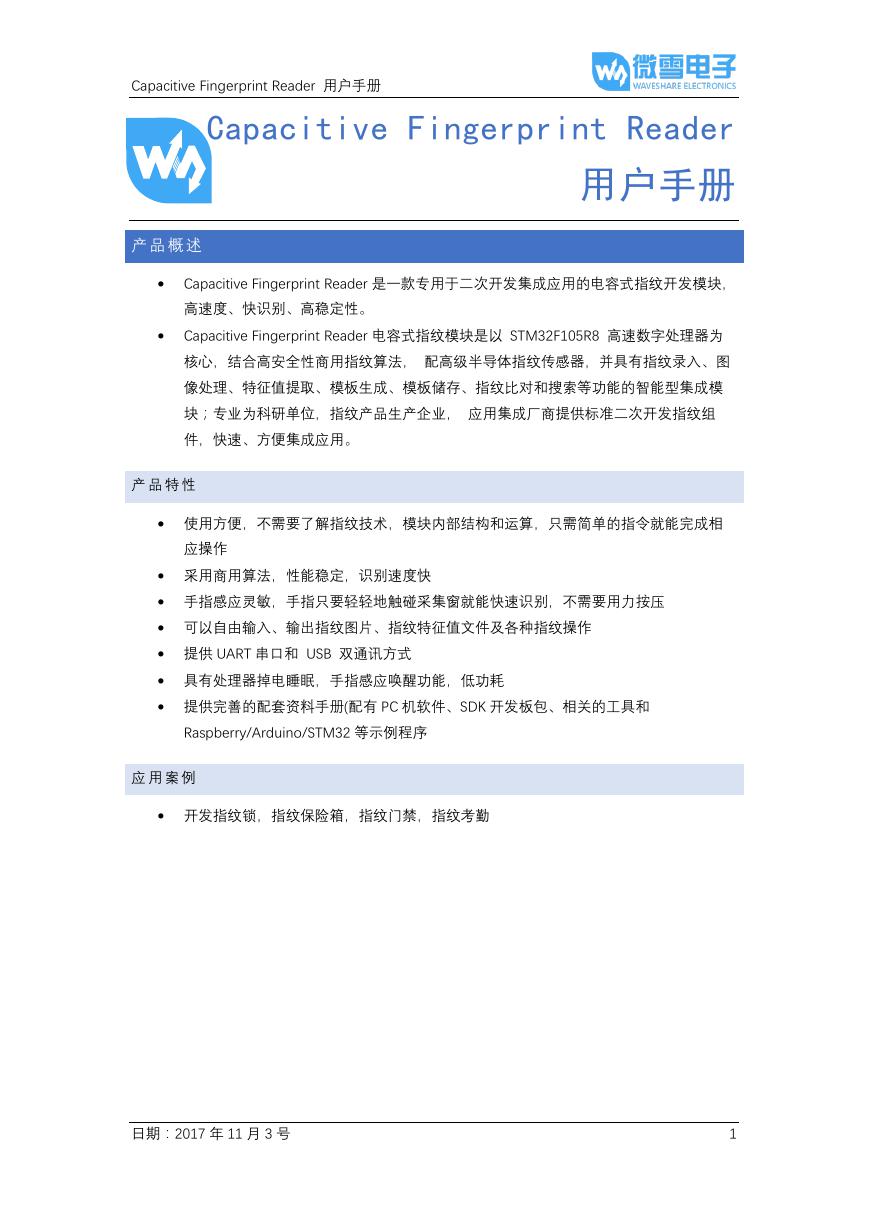 用户手册(Capacitive_Fingerprint_Reader_User_Manual_CN).pdf
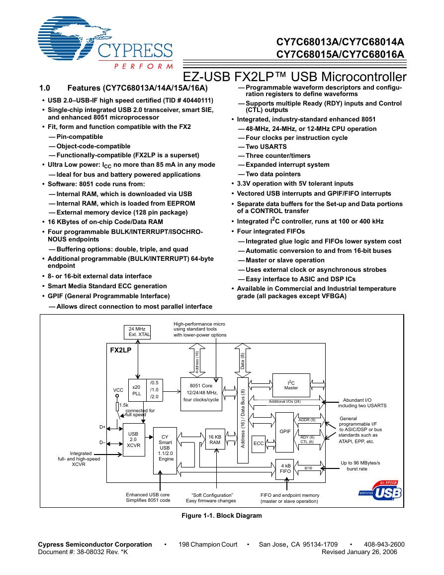 CY7C68013A(英文版)(CY7C68013A).pdf
 TechnicalReference_Dem.pdf