INA219 Zerø-Drift, Bidirectional Current/Power Monitor With I2C Interface
INA219
SBOS448G –AUGUST 2008–REVISED DECEMBER 2015
1 Features
1• Senses Bus Voltages from 0 to 26 V
• Reports Current, Voltage, and Power
•
• High Accuracy: 0.5% (Maximum) Over
16 Programmable Addresses
Temperature (INA219B)
• Filtering Options
• Calibration Registers
• SOT23-8 and SOIC-8 Packages
2 Applications
• Servers
• Telecom Equipment
• Notebook Computers
• Power Management
• Battery Chargers
• Welding Equipment
• Power Supplies
• Test Equipment
3 Description
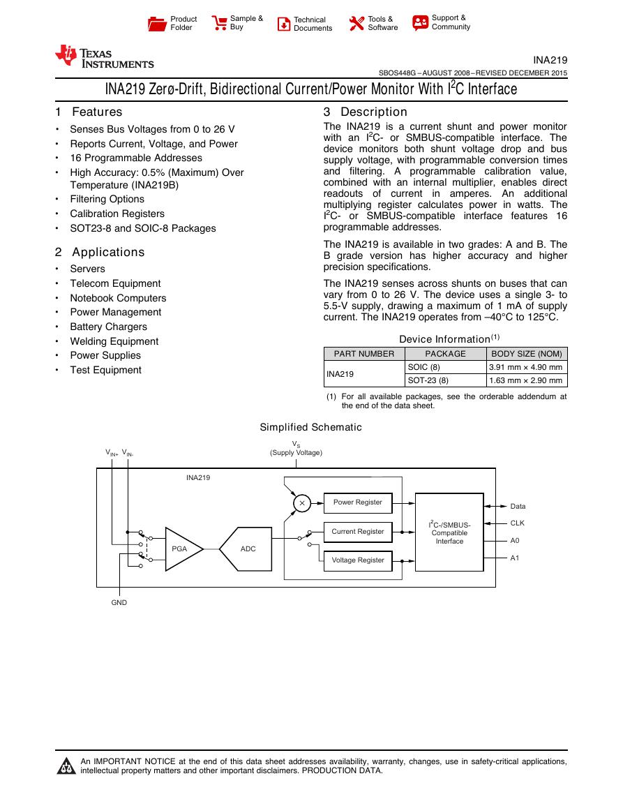
The INA219 is a current shunt and power monitor
with an I2C- or SMBUS-compatible interface. The
device monitors both shunt voltage drop and bus
supply voltage, with programmable conversion times
and filtering. A programmable calibration value,
combined with an internal multiplier, enables direct
readouts of current
in amperes. An additional
multiplying register calculates power in watts. The
I2C- or SMBUS-compatible interface features 16
programmable addresses.
The INA219 is available in two grades: A and B. The
B grade version has higher accuracy and higher
precision specifications.
The INA219 senses across shunts on buses that can
vary from 0 to 26 V. The device uses a single 3- to
5.5-V supply, drawing a maximum of 1 mA of supply
current. The INA219 operates from –40°C to 125°C.
Device Information(1)
PART NUMBER
PACKAGE
INA219
BODY SIZE (NOM)
3.91 mm × 4.90 mm
1.63 mm × 2.90 mm
(1) For all available packages, see the orderable addendum at
SOIC (8)
SOT-23 (8)
the end of the data sheet.
Simplified Schematic
1
An IMPORTANT NOTICE at the end of this data sheet addresses availability, warranty, changes, use in safety-critical applications,
intellectual property matters and other important disclaimers. PRODUCTION DATA.
´Power RegisterCurrent RegisterIC-/SMBUS-CompatibleInterface2Voltage RegisterVIN+VIN-VS(Supply Voltage)A0A1DataCLKADCPGAINA219GNDProductFolderSample &BuyTechnicalDocumentsTools &SoftwareSupport &Community�
INA219
SBOS448G –AUGUST 2008–REVISED DECEMBER 2015
www.ti.com
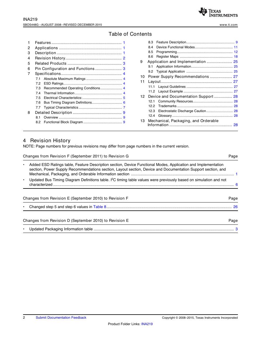
Table of Contents
1
Features.................................................................. 1
2 Applications ........................................................... 1
3 Description ............................................................. 1
4 Revision History..................................................... 2
5 Related Products ................................................... 3
6 Pin Configuration and Functions ......................... 3
7 Specifications......................................................... 4
7.1 Absolute Maximum Ratings ...................................... 4
7.2 ESD Ratings.............................................................. 4
7.3 Recommended Operating Conditions....................... 4
7.4 Thermal Information.................................................. 4
7.5 Electrical Characteristics:.......................................... 5
7.6 Bus Timing Diagram Definitions................................ 6
7.7 Typical Characteristics.............................................. 7
8 Detailed Description .............................................. 9
8.1 Overview ................................................................... 9
8.2 Functional Block Diagram ......................................... 9
8.3 Feature Description................................................... 9
8.4 Device Functional Modes........................................ 11
8.5 Programming........................................................... 12
8.6 Register Maps ........................................................ 18
9 Application and Implementation ........................ 25
9.1 Application Information............................................ 25
9.2 Typical Application ................................................. 25
10 Power Supply Recommendations ..................... 27
11 Layout................................................................... 27
11.1 Layout Guidelines ................................................. 27
11.2 Layout Example .................................................... 27
12 Device and Documentation Support ................. 28
12.1 Community Resources.......................................... 28
12.2 Trademarks ........................................................... 28
12.3 Electrostatic Discharge Caution............................ 28
12.4 Glossary ................................................................ 28
13 Mechanical, Packaging, and Orderable
Information ........................................................... 28
4 Revision History
NOTE: Page numbers for previous revisions may differ from page numbers in the current version.
Changes from Revision F (September 2011) to Revision G
Page
• Added ESD Ratings table, Feature Description section, Device Functional Modes, Application and Implementation
section, Power Supply Recommendations section, Layout section, Device and Documentation Support section, and
Mechanical, Packaging, and Orderable Information section ................................................................................................. 1
• Updated Bus Timing Diagram Definitions table. I2C timing table values were previously based on simulation and not
characterized .......................................................................................................................................................................... 6
Changes from Revision E (September 2010) to Revision F
Page
• Changed step 5 and step 6 values in Table 8...................................................................................................................... 26
Changes from Revision D (September 2010) to Revision E
Page
• Updated Packaging Information table .................................................................................................................................... 3
2
Submit Documentation Feedback
Copyright © 2008–2015, Texas Instruments Incorporated
Product Folder Links: INA219
�
www.ti.com
5 Related Products
INA219
SBOS448G –AUGUST 2008–REVISED DECEMBER 2015
DEVICE
INA209
INA210, INA211, INA212, INA213, INA214
Current/power monitor with watchdog, peak-hold, and fast comparator functions
Zerø-drift, low-cost, analog current shunt monitor series in small package
DESCRIPTION
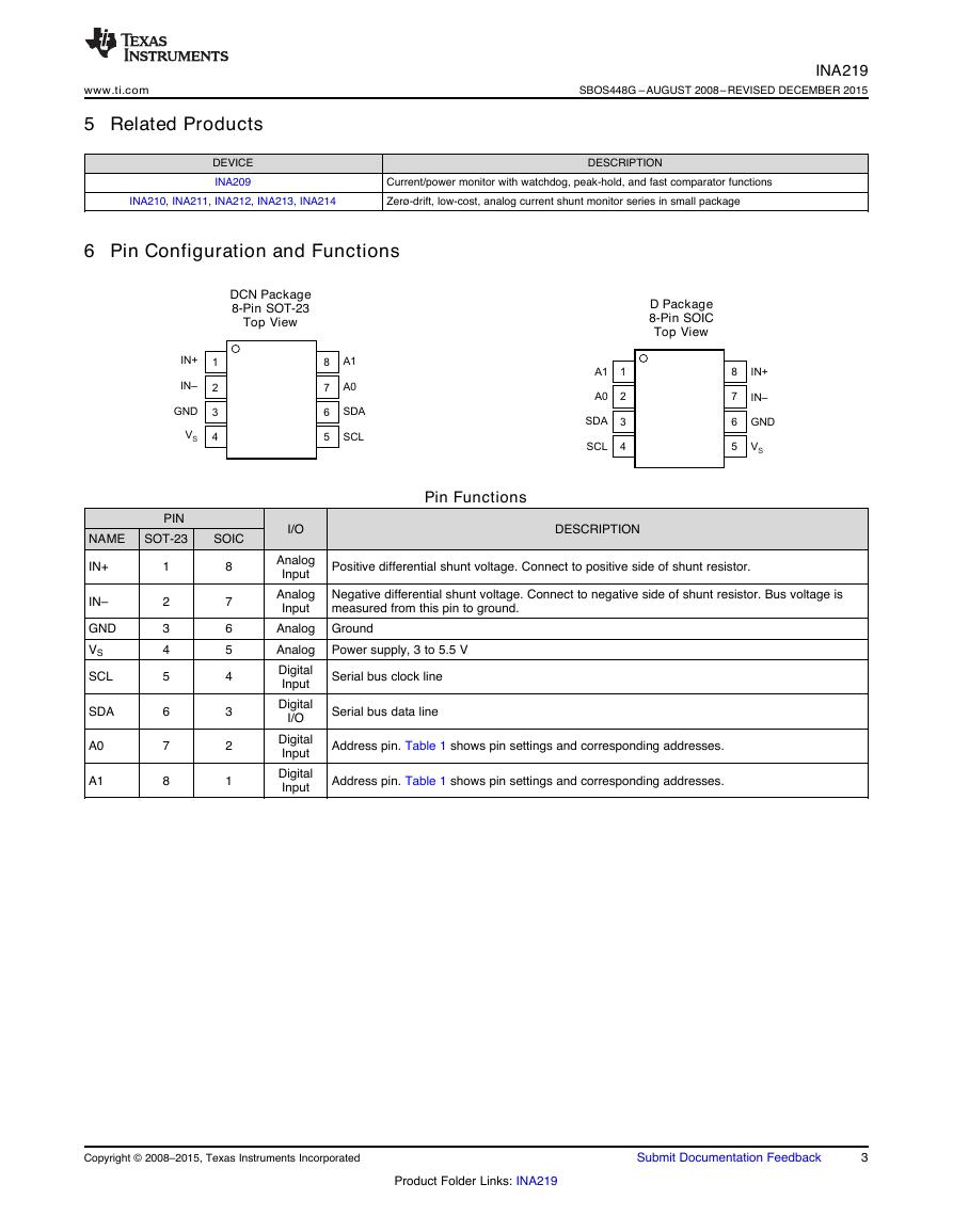
6 Pin Configuration and Functions
DCN Package
8-Pin SOT-23
Top View
D Package
8-Pin SOIC
Top View
PIN
SOT-23
NAME
SOIC
I/O
Pin Functions
DESCRIPTION
IN+
IN–
GND
VS
SCL
SDA
A0
A1
1
2
3
4
5
6
7
8
8
7
6
5
4
3
2
1
measured from this pin to ground.
Positive differential shunt voltage. Connect to positive side of shunt resistor.
Analog
Input
Analog Negative differential shunt voltage. Connect to negative side of shunt resistor. Bus voltage is
Input
Analog Ground
Analog
Digital
Input
Digital
I/O
Serial bus data line
Power supply, 3 to 5.5 V
Serial bus clock line
Digital
Input
Digital
Input
Address pin. Table 1 shows pin settings and corresponding addresses.
Address pin. Table 1 shows pin settings and corresponding addresses.
Copyright © 2008–2015, Texas Instruments Incorporated
Submit Documentation Feedback
3
Product Folder Links: INA219
12348765IN+IN–GNDVSA1A0SDASCL12348765A1A0SDASCLIN+IN–GNDVS�
INA219
SBOS448G –AUGUST 2008–REVISED DECEMBER 2015
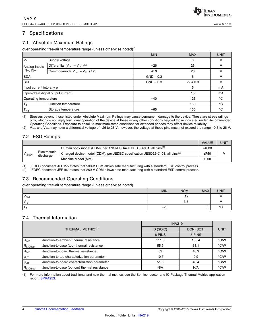
7 Specifications
7.1 Absolute Maximum Ratings
over operating free-air temperature range (unless otherwise noted)(1)
www.ti.com
MIN
MAX
UNIT
Supply voltage
Differential (VIN+ – VIN–)(2)
Common-mode(VIN+ + VIN–) / 2
VS
Analog Inputs
IN+, IN–
SDA
SCL
Input current into any pin
Open-drain digital output current
Operating temperature
TJ
Tstg
(1) Stresses beyond those listed under Absolute Maximum Ratings may cause permanent damage to the device. These are stress ratings
Junction temperature
Storage temperature
V
V
V
V
V
mA
mA
°C
°C
°C
GND – 0.3
GND – 0.3
–40
–65
6
26
26
6
5
10
125
150
150
VS + 0.3
–26
-0.3
only, which do not imply functional operation of the device at these or any other conditions beyond those indicated under Recommended
Operating Conditions. Exposure to absolute-maximum-rated conditions for extended periods may affect device reliability.
(2) VIN+ and VIN– may have a differential voltage of –26 to 26 V; however, the voltage at these pins must not exceed the range –0.3 to 26 V.
7.2 ESD Ratings
V(ESD)
Electrostatic
discharge
Human body model (HBM), per ANSI/ESDA/JEDEC JS-001, all pins(1)
Charged device model (CDM), per JEDEC specification JESD22-C101, all pins(2)
Machine Model (MM)
(1)
(2)
JEDEC document JEP155 states that 500-V HBM allows safe manufacturing with a standard ESD control process.
JEDEC document JEP157 states that 250-V CDM allows safe manufacturing with a standard ESD control process.
VALUE
±4000
±750
±200
UNIT
V
7.3 Recommended Operating Conditions
over operating free-air temperature range (unless otherwise noted)
MIN
–25
NOM
12
3.3
MAX
UNIT
V
V
ºC
85
INA219
DCN (SOT)
UNIT
VCM
V S
TA
7.4 Thermal Information
THERMAL METRIC(1)
Junction-to-ambient thermal resistance
Junction-to-case (top) thermal resistance
Junction-to-board thermal resistance
Junction-to-top characterization parameter
Junction-to-board characterization parameter
Junction-to-case (bottom) thermal resistance
RθJA
RθJC(top)
RθJB
ψJT
ψJB
RθJC(bot)
(1) For more information about traditional and new thermal metrics, see the Semiconductor and IC Package Thermal Metrics application
°C/W
°C/W
°C/W
°C/W
°C/W
°C/W
report, SPRA953.
8 PINS
135.4
68.1
48.9
9.9
48.4
N/A
D (SOIC)
8 PINS
111.3
55.9
52
10.7
51.5
N/A
4
Submit Documentation Feedback
Copyright © 2008–2015, Texas Instruments Incorporated
Product Folder Links: INA219
�
www.ti.com
INA219
SBOS448G –AUGUST 2008–REVISED DECEMBER 2015
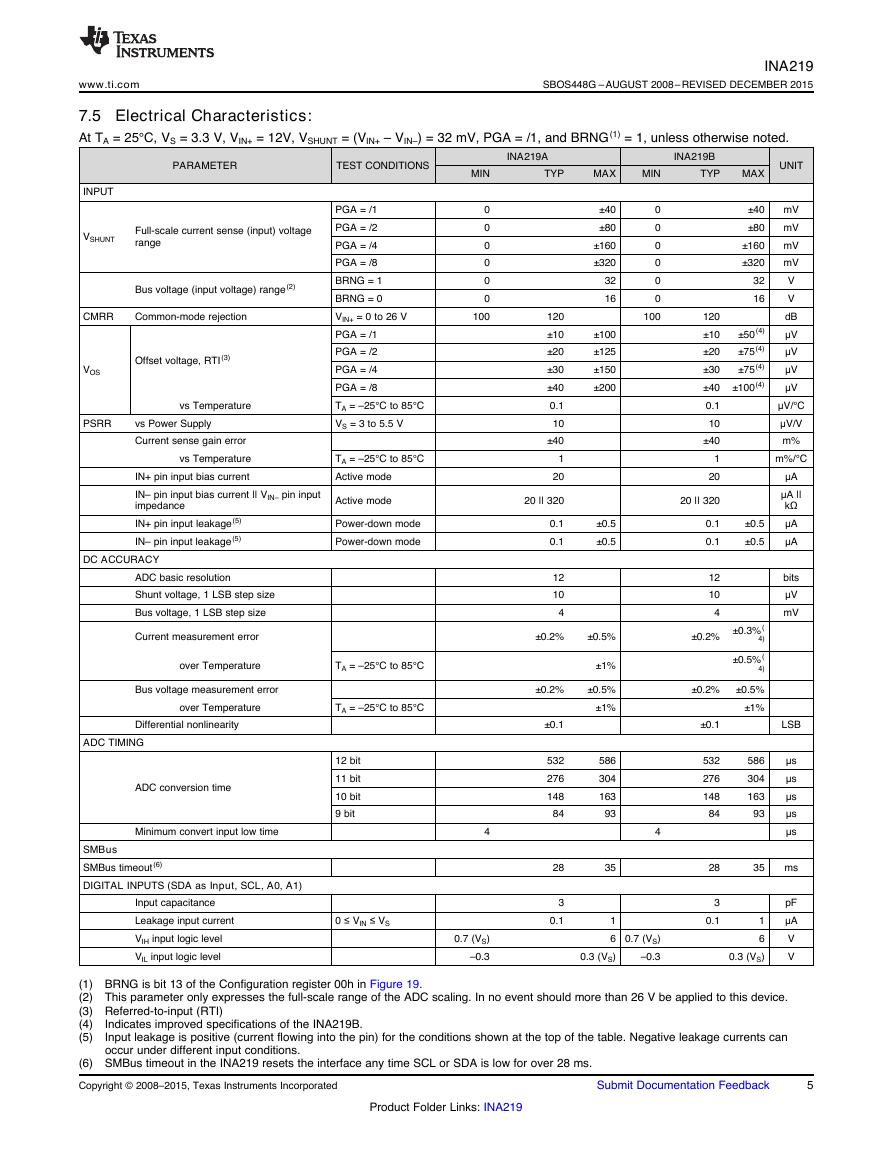
7.5 Electrical Characteristics:
At TA = 25°C, VS = 3.3 V, VIN+ = 12V, VSHUNT = (VIN+ – VIN–) = 32 mV, PGA = /1, and BRNG(1) = 1, unless otherwise noted.
PARAMETER
TEST CONDITIONS
INPUT
VSHUNT
Full-scale current sense (input) voltage
range
Bus voltage (input voltage) range(2)
CMRR
Common-mode rejection
VOS
PSRR
Offset voltage, RTI(3)
vs Temperature
vs Power Supply
Current sense gain error
vs Temperature
IN+ pin input bias current
IN– pin input bias current || VIN– pin input
impedance
IN+ pin input leakage(5)
IN– pin input leakage(5)
DC ACCURACY
ADC basic resolution
Shunt voltage, 1 LSB step size
Bus voltage, 1 LSB step size
Current measurement error
PGA = /1
PGA = /2
PGA = /4
PGA = /8
BRNG = 1
BRNG = 0
VIN+ = 0 to 26 V
PGA = /1
PGA = /2
PGA = /4
PGA = /8
TA = –25°C to 85°C
VS = 3 to 5.5 V
TA = –25°C to 85°C
Active mode
Active mode
Power-down mode
Power-down mode
MIN
0
0
0
0
0
0
100
INA219A
TYP
MAX
MIN
INA219B
TYP
0
0
0
0
0
0
100
±40
±80
±160
±320
32
16
±100
±125
±150
±200
120
±10
±20
±30
±40
0.1
10
±40
1
20
120
±10
±20
±30
±40
0.1
10
±40
1
20
20 || 320
20 || 320
±0.5
±0.5
0.1
0.1
12
10
4
0.1
0.1
12
10
4
±0.2%
±0.5%
±0.2%
UNIT
mV
mV
mV
mV
V
V
dB
μV
μV
μV
μV
μV/°C
μV/V
m%
m%/°C
μA
μA ||
kΩ
μA
μA
bits
μV
mV
MAX
±40
±80
±160
±320
32
16
±50(4)
±75(4)
±75(4)
±100(4)
±0.5
±0.5
±0.3%(
4)
±0.5%(
4)
over Temperature
TA = –25°C to 85°C
Bus voltage measurement error
over Temperature
TA = –25°C to 85°C
±0.2%
±1%
±0.5%
±1%
Differential nonlinearity
ADC TIMING
ADC conversion time
Minimum convert input low time
SMBus
SMBus timeout(6)
DIGITAL INPUTS (SDA as Input, SCL, A0, A1)
Input capacitance
Leakage input current
VIH input logic level
VIL input logic level
12 bit
11 bit
10 bit
9 bit
0 ≤ VIN ≤ VS
±0.1
532
276
148
84
28
3
0.1
586
304
163
93
35
4
1
6 0.7 (VS)
–0.3
0.3 (VS)
4
0.7 (VS)
–0.3
±0.2% ±0.5%
±1%
±0.1
532
276
148
84
28
3
0.1
LSB
μs
μs
μs
μs
μs
586
304
163
93
35
ms
pF
μA
V
V
1
6
0.3 (VS)
(1) BRNG is bit 13 of the Configuration register 00h in Figure 19.
(2) This parameter only expresses the full-scale range of the ADC scaling. In no event should more than 26 V be applied to this device.
(3) Referred-to-input (RTI)
(4)
(5)
Indicates improved specifications of the INA219B.
Input leakage is positive (current flowing into the pin) for the conditions shown at the top of the table. Negative leakage currents can
occur under different input conditions.
(6) SMBus timeout in the INA219 resets the interface any time SCL or SDA is low for over 28 ms.
Copyright © 2008–2015, Texas Instruments Incorporated
Submit Documentation Feedback
5
Product Folder Links: INA219
�
INA219
SBOS448G –AUGUST 2008–REVISED DECEMBER 2015
www.ti.com
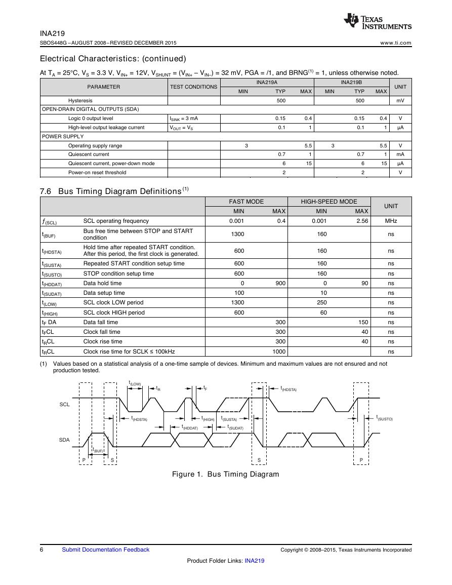
Electrical Characteristics: (continued)
At TA = 25°C, VS = 3.3 V, VIN+ = 12V, VSHUNT = (VIN+ – VIN–) = 32 mV, PGA = /1, and BRNG(1) = 1, unless otherwise noted.
PARAMETER
TEST CONDITIONS
Hysteresis
OPEN-DRAIN DIGITAL OUTPUTS (SDA)
Logic 0 output level
High-level output leakage current
ISINK = 3 mA
VOUT = VS
POWER SUPPLY
Operating supply range
Quiescent current
Quiescent current, power-down mode
Power-on reset threshold
7.6 Bus Timing Diagram Definitions(1)
MIN
3
INA219A
TYP
500
0.15
0.1
0.7
6
2
MAX
MIN
INA219B
TYP
500
0.4
1
5.5
1
15
3
0.15
0.1
0.7
6
2
FAST MODE
HIGH-SPEED MODE
MIN
0.001
1300
MAX
0.4
MIN
0.001
160
MAX
2.56
UNIT
MAX
mV
V
μA
V
mA
μA
V
0.4
1
5.5
1
15
UNIT
MHz
600
ƒ(SCL)
t(BUF)
SCL operating frequency
Bus free time between STOP and START
condition
Hold time after repeated START condition.
After this period, the first clock is generated.
Repeated START condition setup time
STOP condition setup time
Data hold time
Data setup time
SCL clock LOW period
SCL clock HIGH period
Data fall time
Clock fall time
Clock rise time
Clock rise time for SCLK ≤ 100kHz
t(HDSTA)
t(SUSTA)
t(SUSTO)
t(HDDAT)
t(SUDAT)
t(LOW)
t(HIGH)
tF DA
tFCL
tRCL
tRCL
(1) Values based on a statistical analysis of a one-time sample of devices. Minimum and maximum values are not ensured and not
600
600
0
100
1300
600
160
160
160
0
10
250
60
90
150
40
40
900
300
300
300
1000
ns
ns
ns
ns
ns
ns
ns
ns
ns
ns
ns
ns
production tested.
Figure 1. Bus Timing Diagram
6
Submit Documentation Feedback
Copyright © 2008–2015, Texas Instruments Incorporated
Product Folder Links: INA219
SCLSDAt(LOW)tRtFt(HDSTA)t(HDSTA)t(HDDAT)t(BUF)t(SUDAT)t(HIGH)t(SUSTA)t(SUSTO)PSSP�
www.ti.com
INA219
SBOS448G –AUGUST 2008–REVISED DECEMBER 2015
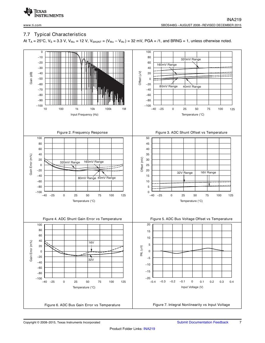
7.7 Typical Characteristics
At TA = 25°C, VS = 3.3 V, VIN+ = 12 V, VSHUNT = (VIN+ – VIN–) = 32 mV, PGA = /1, and BRNG = 1, unless otherwise noted.
Figure 2. Frequency Response
Figure 3. ADC Shunt Offset vs Temperature
Figure 4. ADC Shunt Gain Error vs Temperature
Figure 5. ADC Bus Voltage Offset vs Temperature
Figure 6. ADC Bus Gain Error vs Temperature
Figure 7. Integral Nonlinearity vs Input Voltage
Copyright © 2008–2015, Texas Instruments Incorporated
Submit Documentation Feedback
7
Product Folder Links: INA219
-40-250255075100125100806040200-20-40-60-80-100Gain Error (m%)Temperature (C)°32V16V20151050-5-10-15-20-0.4-0.3-0.2-0.100.10.20.3INL (V)mInput Voltage (V)0.4100806040200-20-40-60-80-100-40-250255075100Gain Error (m%)Temperature (C)°125320mV Range160mV Range80mV Range40mV Range50454035302520151050-40-250255075100Offset (mV)Temperature (C)°12532V Range16V Range0-10-20-30-40-50-60-70-80-90-100101001k10k100k1MGain (dB)Input Frequency (Hz)100806040200-20-40-60-80-100-40-250255075100Offset (V)mTemperature (C)°125160mV Range320mV Range80mV Range40mV Range�
INA219
SBOS448G –AUGUST 2008–REVISED DECEMBER 2015
www.ti.com
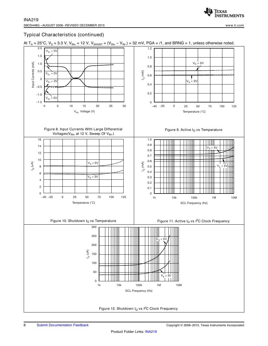
Typical Characteristics (continued)
At TA = 25°C, VS = 3.3 V, VIN+ = 12 V, VSHUNT = (VIN+ – VIN–) = 32 mV, PGA = /1, and BRNG = 1, unless otherwise noted.
Figure 8. Input Currents With Large Differential
Voltages(VIN+ at 12 V, Sweep Of VIN–)
Figure 9. Active IQ vs Temperature
Figure 10. Shutdown IQ vs Temperature
Figure 11. Active IQ vs I2C Clock Frequency
Figure 12. Shutdown IQ vs I2C Clock Frequency
8
Submit Documentation Feedback
Copyright © 2008–2015, Texas Instruments Incorporated
Product Folder Links: INA219
3002502001501005001k10k100k1M10MI(A)QmSCL Frequency (Hz)V= 5VSV= 3VS1.00.90.80.70.60.50.40.30.20.101k10k100k1M10MIQ(mA)SCL Frequency (Hz)V= 5VSV=S3V1614121086420-40-25025125I(A)mQTemperature (C)°V= 5VSV= 3VS50751001.21.00.80.60.40.20-40-250255075100I(mA)QTemperature (C)°125V= 3VSV= 5VS2.01.51.00.50-0.5-1.0-1.50510152025Input Currents (mA)VVoltage (V)IN-30VS+= 5VV5VS+=VS+= 3VV3VS+=�


 V2版本原理图(Capacitive-Fingerprint-Reader-Schematic_V2).pdf
 摄像头工作原理.doc
 VL53L0X简要说明(En.FLVL53L00216).pdf
 原理图(DVK720-Schematic).pdf
 原理图(Pico-Clock-Green-Schdoc).pdf
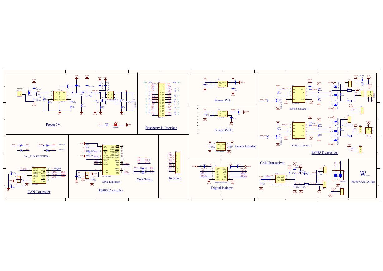 原理图(RS485-CAN-HAT-B-schematic).pdf
 File:SIM7500_SIM7600_SIM7800 Series_SSL_Application Note_V2.00.pdf
 ADS1263(Ads1262).pdf
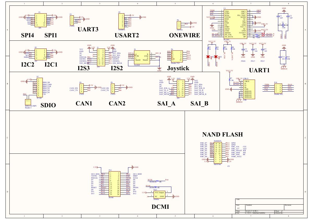 原理图(Open429Z-D-Schematic).pdf
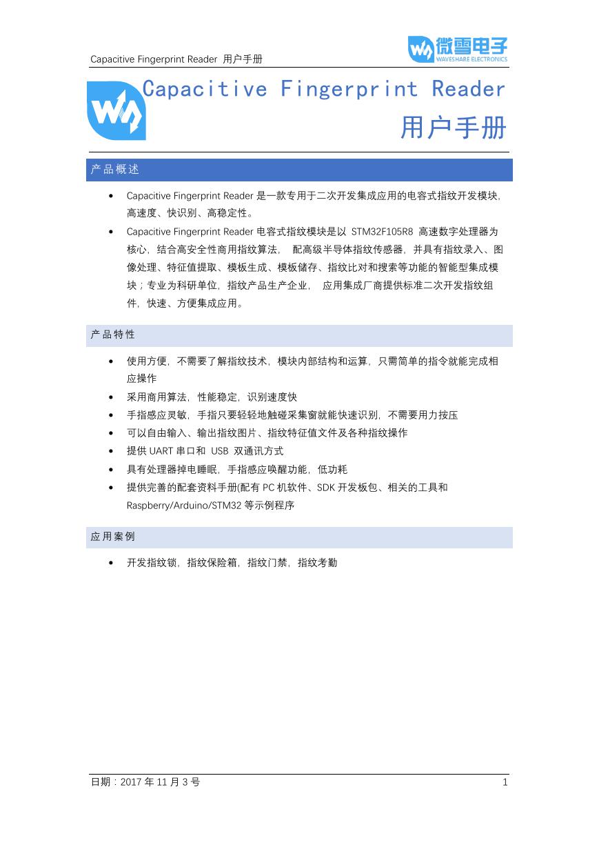 用户手册(Capacitive_Fingerprint_Reader_User_Manual_CN).pdf
 CY7C68013A(英文版)(CY7C68013A).pdf
 TechnicalReference_Dem.pdf