HY2213
Datasheet
1 Cell Li-ion/Polymer Battery Charge Balance IC
.
© 2012 -2015 HYCON Technology Corp.
www.hycontek.com
DS-HY2213-V05_EN
�
HY2213
1 Cell Li Battery Charge Balance IC
Table of Contents
1. GENERAL DESCRIPTION
....................................................................................................................... 4
2.
FEATURE
.................................................................................................................................................. 4
3. APPLICATION
.......................................................................................................................................... 4
4. BLOCK DIAGRAM
.................................................................................................................................... 5
5. ORDERING INFORMATION
..................................................................................................................... 5
6. MODEL LIST
............................................................................................................................................. 6
6.1.
6.2.
Electrical Parameter Option
Characteristic Code- Other Function Option
.................................................................................................................. 6
......................................................................................... 6
7. PIN CONFIGURATION AND PACKAGE MARKING INFORMATION
..................................................... 6
8. ELECTRICAL CHARACTERISTICS
........................................................................................................ 7
8.1.
8.2.
Absolute Maximum Ratings
Electrical Characteristics (Excluding Delay Time)
.................................................................................................................. 7
................................................................................ 7
9. EXAMPLE CIRCUIT OF BATTERY CHARGE BALANCE IC APPLICATION
......................................... 8
.
10. DESCRIPTION OF OPERATION
............................................................................................................. 9
10.1. Normal Status
10.2. Overcharge Status
10.3. Standby Status
........................................................................................................................................ 9
................................................................................................................................ 9
...................................................................................................................................... 9
11. CHARACTERISTIC CURVE (TYPICAL VALUE)
................................................................................... 10
12. PACKAGE INFORMATION
..................................................................................................................... 11
12.1. SOT-23-6 Package
.............................................................................................................................. 11
13. TAPE & REEL INFORMATION
............................................................................................................... 12
13.1. Tape & Reel Information ---SOT-23-6 (Type 1)
13.2. Tape & Reel Information ---SOT-23-6 (Type 2)
................................................................................... 12
................................................................................... 13
14. REVISION HISTORY
.............................................................................................................................. 14
© 2012-2015 HYCON Technology Corp
www.hycontek.com
DS-HY2213-V05_EN
Page 2
�
HY2213
1 Cell Li Battery Charge Balance IC
Attention:
1. HYCON Technology Corp. reserves the right to change the content of this datasheet without further
notice. For most up-to-date information, please constantly visit our website: http://www.hycontek.com .
2. HYCON Technology Corp. is not responsible for problems caused by figures or application circuits
narrated herein whose related industrial properties belong to third parties.
3. Specifications of any HYCON Technology Corp. products detailed or contained herein stipulate the
performance, characteristics, and functions of the specified products in the independent state. We does
not guarantee of the performance, characteristics, and functions of the specified products as placed in
the customer’s products or equipment. Constant and sufficient verification and evaluation is highly
advised.
4. Please note the operating conditions of input voltage, output voltage and load current and ensure the IC
internal power consumption does not exceed that of package tolerance. HYCON Technology Corp.
assumes no responsibility for equipment failures that resulted from using products at values that exceed,
even momentarily, rated values listed in products specifications of HYCON products specified herein.
5. Notwithstanding this product has built-in ESD protection circuit, please do not exert excessive static
electricity to protection circuit.
6. Products specified or contained herein cannot be employed in applications which require extremely high
levels of reliability, such as device or equipment affecting the human body, health/medical equipments,
security systems, or any apparatus installed in aircrafts and other vehicles.
7. Despite the fact that HYCON Technology Corp. endeavors to enhance product quality as well as
reliability in every possible way, failure or malfunction of semiconductor products may happen. Hence,
users are strongly recommended to comply with safety design including redundancy and fire-precaution
equipments to prevent any accidents and fires that may follow.
.
8. Use of the information described herein for other purposes and/or reproduction or copying without the
permission of HYCON Technology Corp. is strictly prohibited.
© 2012-2015 HYCON Technology Corp
www.hycontek.com
DS-HY2213-V05_EN
Page 3
�
HY2213
1 Cell Li Battery Charge Balance IC
1. General Description
The series of HY2213 is created for multi-cell battery packs to single-cell lithium-ion battery
Charge balance control, electrical level monitoring ICs and it also comprises high-accuracy
voltage detection circuit and delay circuit.
2. Feature
HY2213 series IC equips with the following features:
(1) High Precision Voltage Detection Circuit
Overcharge detection voltage 4.000~4.500V Precision: ±25mV
Overcharge release voltage 3.800~4.500V Precision: ±35mV
Standby detection voltage 2.70V Precision: ±15%
Standby release voltage 2.70V Precision: ±15%
(2) Delay times are generated by an internal circuit (external capacitors are unnecessary).
(3) Low consumption current
Operation mode Typ. value 2.5μA, max. value: 3.5μA (VDD=3.9V)
Standby mode Max. value:0.5μA (VDD=2.7V)
(4) Wide operation temperature range: -40℃~ +85℃
(5) Small package: SOT-23-6
(6) The HY2213 series are Halogen-free, green package
3. Application
.
Multi-cell Li-ion rechargeable battery packs
© 2012-2015 HYCON Technology Corp
www.hycontek.com
DS-HY2213-V05_EN
Page 4
�
HY2213
1 Cell Li Battery Charge Balance IC
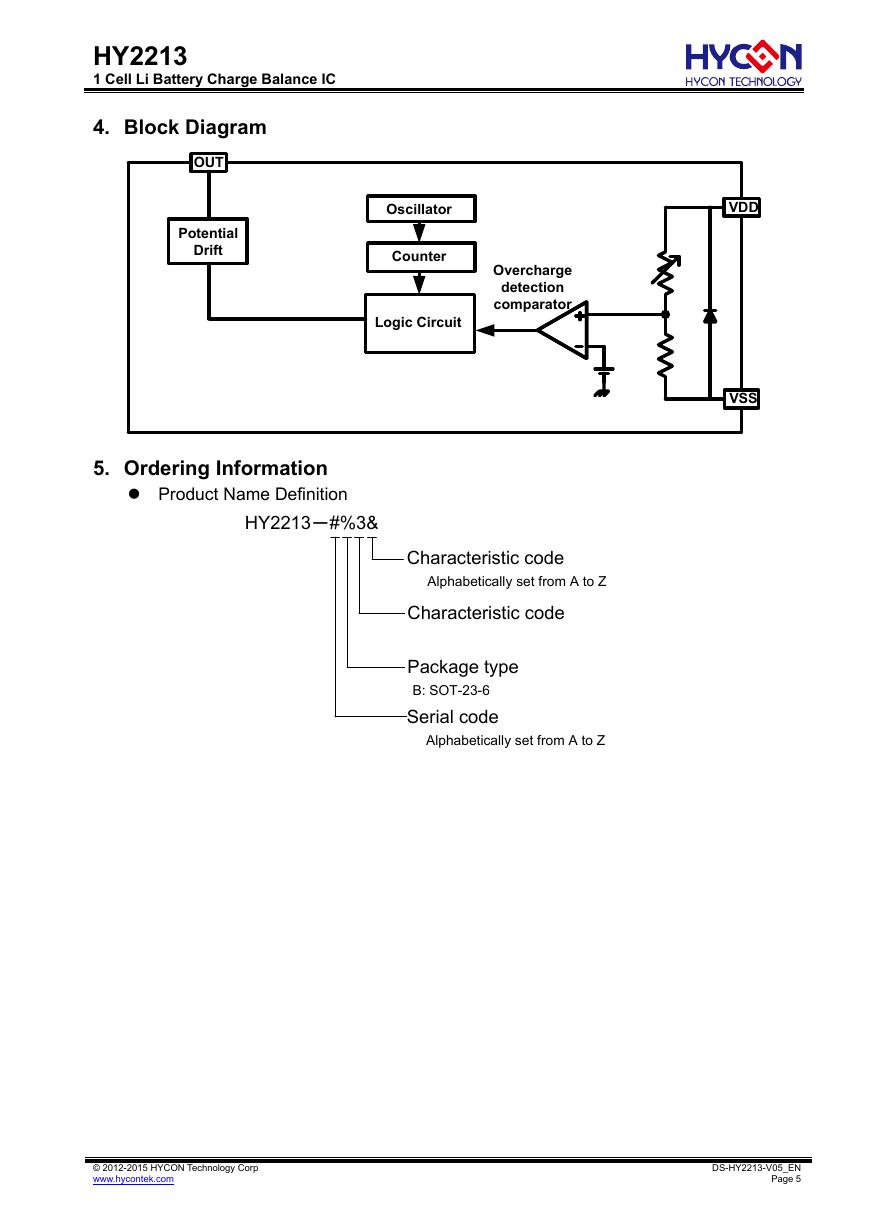
4. Block Diagram
OUT
Potential
Drift
Oscillator
Counter
Logic Circuit
Overcharge
detection
comparator
VDD
VSS
5. Ordering Information
Product Name Definition
HY2213-#%3&
.
Characteristic code
Alphabetically set from A to Z
Characteristic code
Package type
B: SOT-23-6
Serial code
Alphabetically set from A to Z
© 2012-2015 HYCON Technology Corp
www.hycontek.com
DS-HY2213-V05_EN
Page 5
�
HY2213
1 Cell Li Battery Charge Balance IC
6. Model List
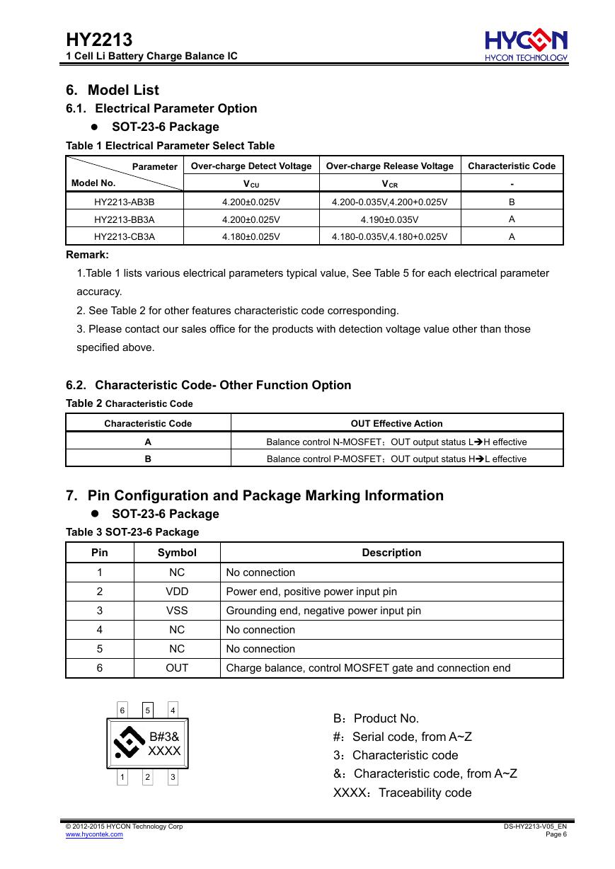
6.1. Electrical Parameter Option
SOT-23-6 Package
Table 1 Electrical Parameter Select Table
Parameter
Over-charge Detect Voltage Over-charge Release Voltage Characteristic Code
Model No.
HY2213-AB3B
HY2213-BB3A
HY2213-CB3A
Remark:
V
CU
4.200±0.025V
4.200±0.025V
4.180±0.025V
V
CR
4.200-0.035V,4.200+0.025V
4.190±0.035V
4.180-0.035V,4.180+0.025V
-
B
A
A
1.Table 1 lists various electrical parameters typical value, See Table 5 for each electrical parameter
accuracy.
2. See Table 2 for other features characteristic code corresponding.
3. Please contact our sales office for the products with detection voltage value other than those
specified above.
6.2. Characteristic Code- Other Function Option
Table 2 Characteristic Code
Characteristic Code
.
OUT Effective Action
A
B
Balance control N-MOSFET;OUT output status LH effective
Balance control P-MOSFET;OUT output status HL effective
7. Pin Configuration and Package Marking Information
SOT-23-6 Package
Table 3 SOT-23-6 Package
Symbol
Pin
1
2
3
4
5
6
Description
NC
VDD
VSS
NC
NC
OUT
No connection
Power end, positive power input pin
Grounding end, negative power input pin
No connection
No connection
Charge balance, control MOSFET gate and connection end
6
5
4
B#3&
XXXX·
1
2
3
B:Product No.
#:Serial code, from A~Z
3:Characteristic code
&:Characteristic code, from A~Z
XXXX:Traceability code
© 2012-2015 HYCON Technology Corp
www.hycontek.com
DS-HY2213-V05_EN
Page 6
�
HY2213
1 Cell Li Battery Charge Balance IC
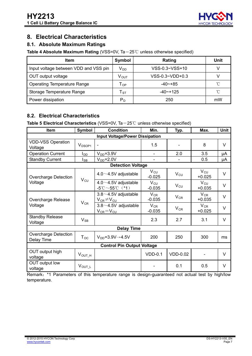
8. Electrical Characteristics
8.1. Absolute Maximum Ratings
Table 4 Absolute Maximum Rating (VSS=0V, Ta=25℃ unless otherwise specified)
Item
Symbol
Rating
Input voltage between VDD and VSS pin
OUT output voltage
Operating Temperature Range
Storage Temperature Range
Power dissipation
DD
V
OUT
V
OP
T
T
ST
D
P
VSS-0.3~VSS+10
VSS-0.3~VDD+0.3
-40~+85
-40~+125
250
8.2. Electrical Characteristics
Table 5 Electrical Characteristics (VSS=0V, Ta=25℃ unless otherwise specified)
Unit
V
V
℃
℃
mW
Item
Symbol
Condition
Min.
Typ.
Max.
Unit
VDD-VSS Operation
Voltage
Operation Current
Standby Current
V
DSOP1
DD
I
I
SB
Overcharge Detection
Voltage
V
CU
Overcharge Release
Voltage
Standby Release
Voltage
V
CR
V
SB
-
2.0
-
V
CU
V
CU
V
CR
V
CR
2.7
8
3.5
0.5
V
CU
+0.025
V
CU
+0.035
V
CR
+0.035
V
CR
+0.025
3.1
V
μA
μA
V
V
V
V
V
250
300
ms
Input Voltage/Power Dissipation
-
V
V
=3.9V
=2.0V
1.5
-
-
DD
DD
Detection Voltage
.
4.0~4.5V adjustable
4.0~4.5V adjustable
-5℃~55℃(*1)
3.8~4.5V adjustable
VCR≠V
3.8~4.5V adjustable
VCR=V
CU
CU
Delay Time
VCU
-0.025
VCU
-0.035
V
-0.035
V
-0.035
CR
CR
2.3
Overcharge Detection
Delay Time
T
OC
V
=3.9V→4.5V
200
DD
Control Pin Output Voltage
V
OUT_H
OUT output high
voltage
OUT output low
voltage
Remark:*1 Parameters of this temperature range is design-guaranteed not actual test by high/low
temperature.
VDD-0.1 VDD-0.02
OUT_L
0.1
0.5
V
V
V
-
-
© 2012-2015 HYCON Technology Corp
www.hycontek.com
DS-HY2213-V05_EN
Page 7
�
HY2213
1 Cell Li Battery Charge Balance IC
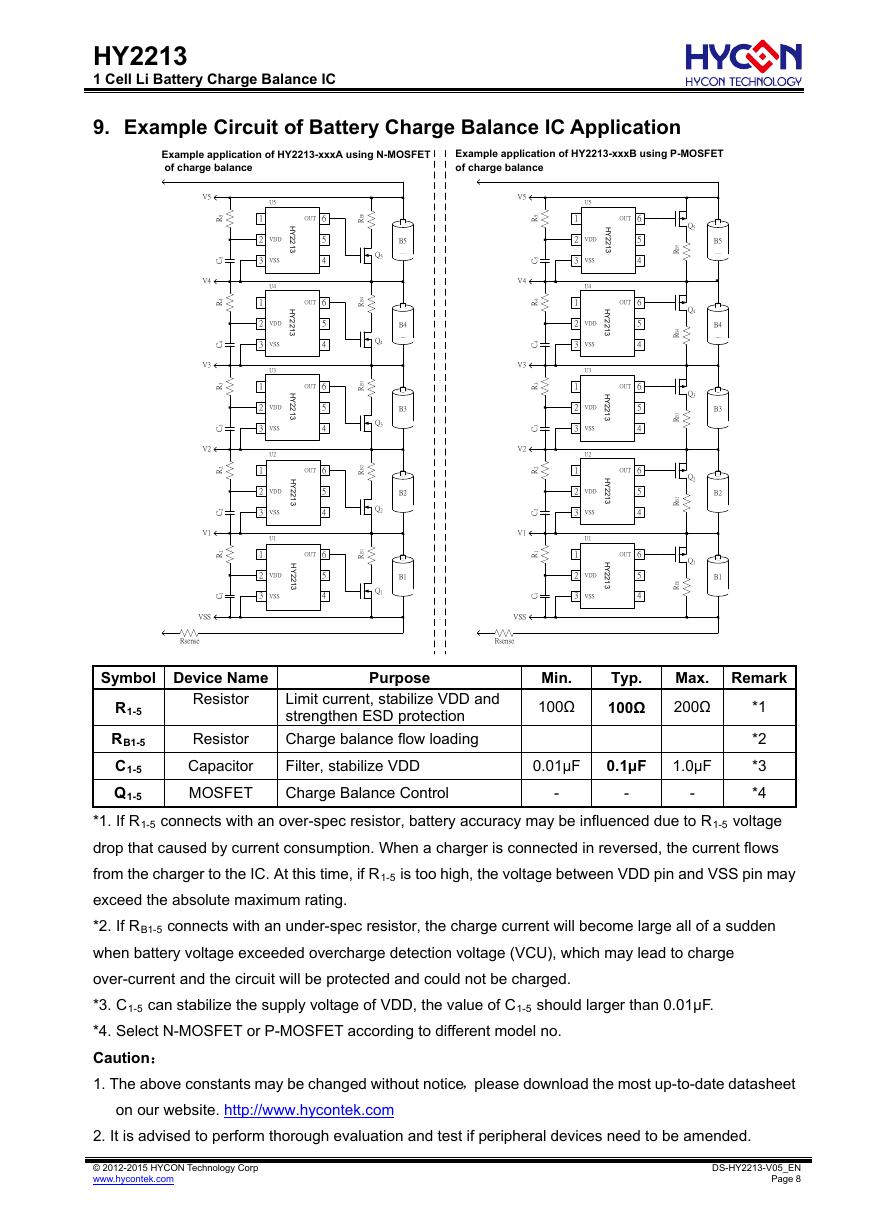
9. Example Circuit of Battery Charge Balance IC Application
Example application of HY2213-xxxA using N-MOSFET
of charge balance
Example application of HY2213-xxxB using P-MOSFET
of charge balance
V5
V4
V3
V2
V1
5
R
5
C
4
R
4
C
3
R
3
C
2
R
2
C
1
R
1
C
VSS
Rsense
U5
VDD
VSS
U4
VDD
VSS
U3
VDD
VSS
U2
VDD
VSS
U1
VDD
VSS
1
2
3
1
2
3
1
2
3
1
2
3
1
2
3
H
Y
2
2
1
3
H
Y
2
2
1
3
H
Y
2
2
1
3
H
Y
2
2
1
3
H
Y
2
2
1
3
OUT
OUT
OUT
OUT
OUT
6
5
4
6
5
4
6
5
4
6
5
4
6
5
4
5
B
R
4
B
R
3
B
R
2
B
R
1
B
R
B5
Q5
B4
Q4
B3
Q3
B2
Q2
B1
Q1
.
V5
V4
V3
V2
V1
5
R
5
C
4
R
4
C
3
R
3
C
2
R
2
C
1
R
1
C
VSS
Rsense
U5
VDD
VSS
U4
VDD
VSS
U3
VDD
VSS
U2
VDD
VSS
U1
VDD
VSS
1
2
3
1
2
3
1
2
3
1
2
3
1
2
3
OUT
H
Y
2
2
1
3
OUT
OUT
OUT
OUT
H
Y
2
2
1
3
H
Y
2
2
1
3
H
Y
2
2
1
3
H
Y
2
2
1
3
6
5
4
6
5
4
6
5
4
6
5
4
6
5
4
Q5
Q4
Q3
Q2
Q1
5
B
R
4
B
R
3
B
R
2
B
R
1
B
R
B5
B4
B3
B2
B1
Min.
100Ω
Typ.
100Ω
0.01μF
0.1μF
1.0μF
-
-
-
Max. Remark
200Ω
*1
*2
*3
*4
Symbol Device Name
R
1-5
B1-5
R
C
1-5
Q1-5
Resistor
Resistor
Capacitor
MOSFET
Purpose
Limit current, stabilize VDD and
strengthen ESD protection
Charge balance flow loading
Filter, stabilize VDD
Charge Balance Control
B1-5
is too high, the voltage between VDD pin and VSS pin may
connects with an under-spec resistor, the charge current will become large all of a sudden
*1. If R1-5 connects with an over-spec resistor, battery accuracy may be influenced due to R1-5 voltage
drop that caused by current consumption. When a charger is connected in reversed, the current flows
from the charger to the IC. At this time, if R1-5
exceed the absolute maximum rating.
*2. If R
when battery voltage exceeded overcharge detection voltage (VCU), which may lead to charge
over-current and the circuit will be protected and could not be charged.
*3. C
*4. Select N-MOSFET or P-MOSFET according to different model no.
Caution:
1. The above constants may be changed without notice,please download the most up-to-date datasheet
1-5 can stabilize the supply voltage of VDD, the value of C1-5
should larger than 0.01μF.
on our website. http://www.hycontek.com
2. It is advised to perform thorough evaluation and test if peripheral devices need to be amended.
© 2012-2015 HYCON Technology Corp
www.hycontek.com
DS-HY2213-V05_EN
Page 8
�


 V2版本原理图(Capacitive-Fingerprint-Reader-Schematic_V2).pdf
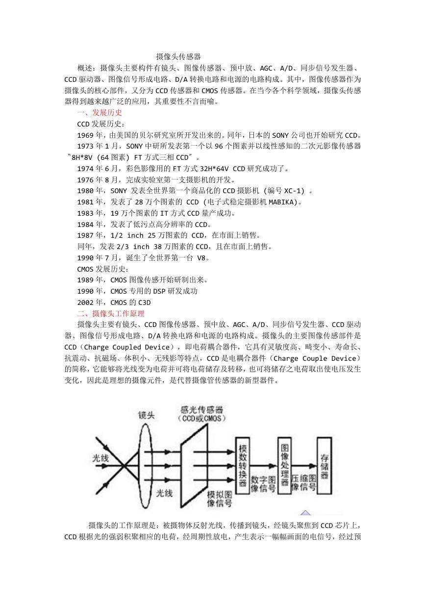 摄像头工作原理.doc
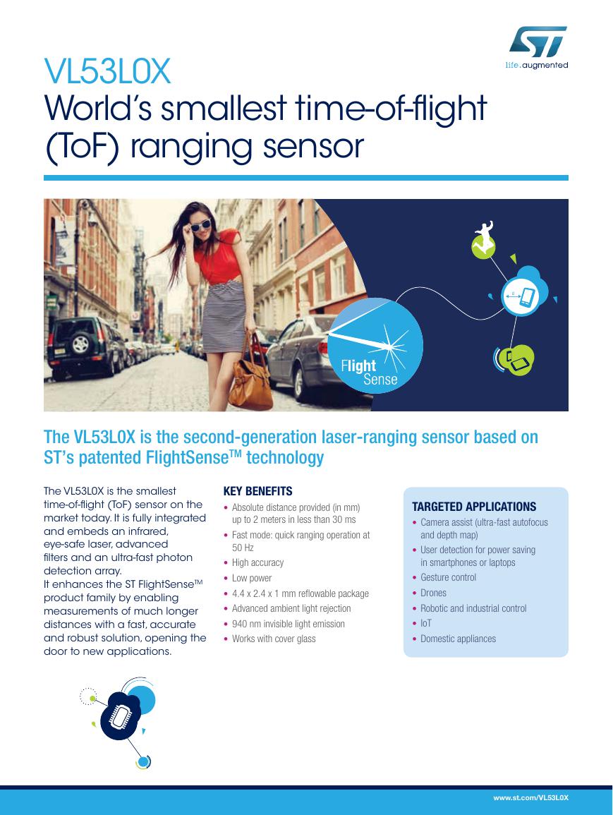 VL53L0X简要说明(En.FLVL53L00216).pdf
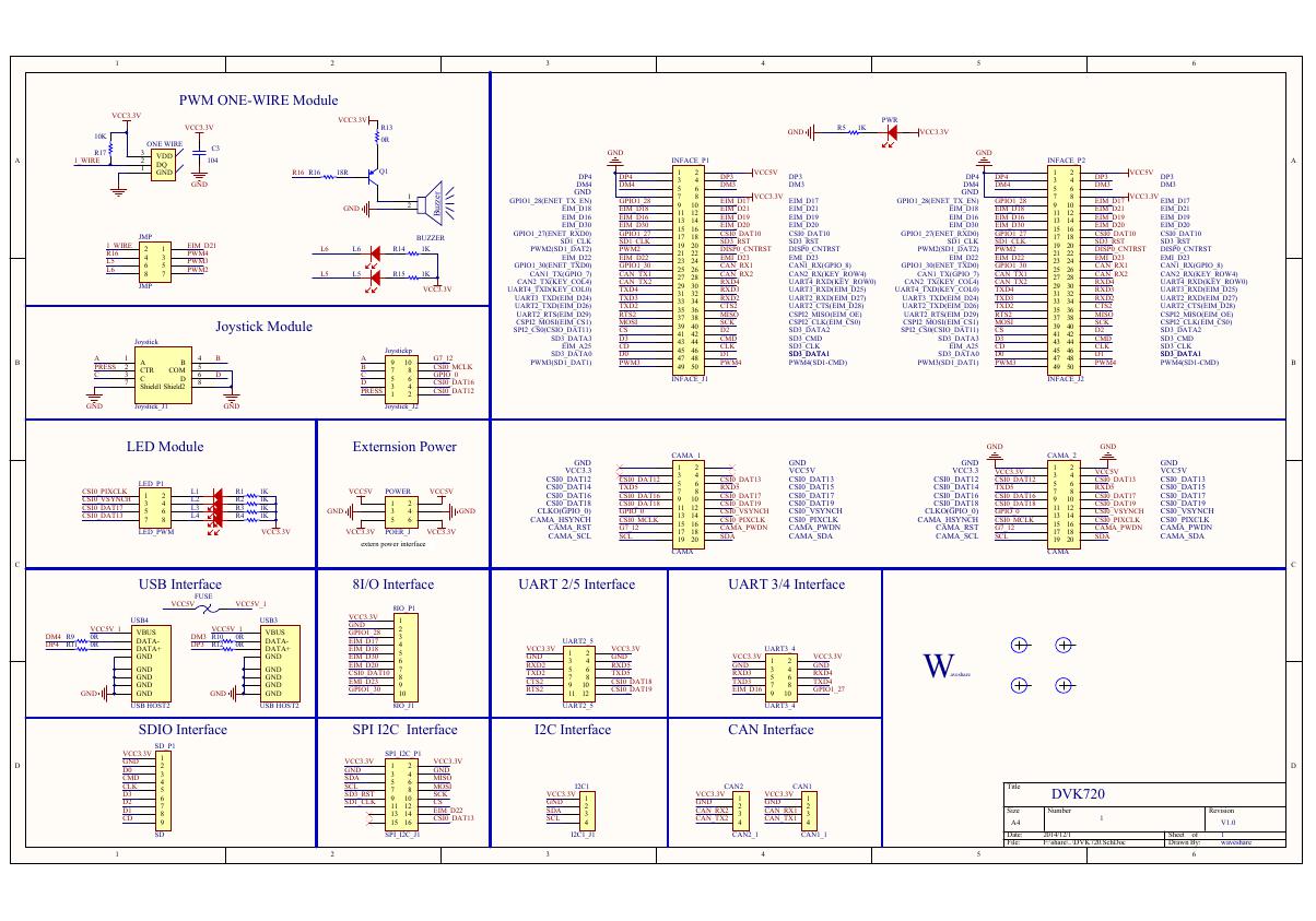 原理图(DVK720-Schematic).pdf
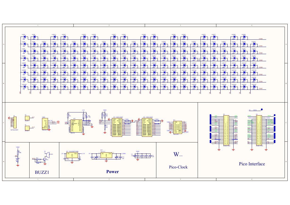 原理图(Pico-Clock-Green-Schdoc).pdf
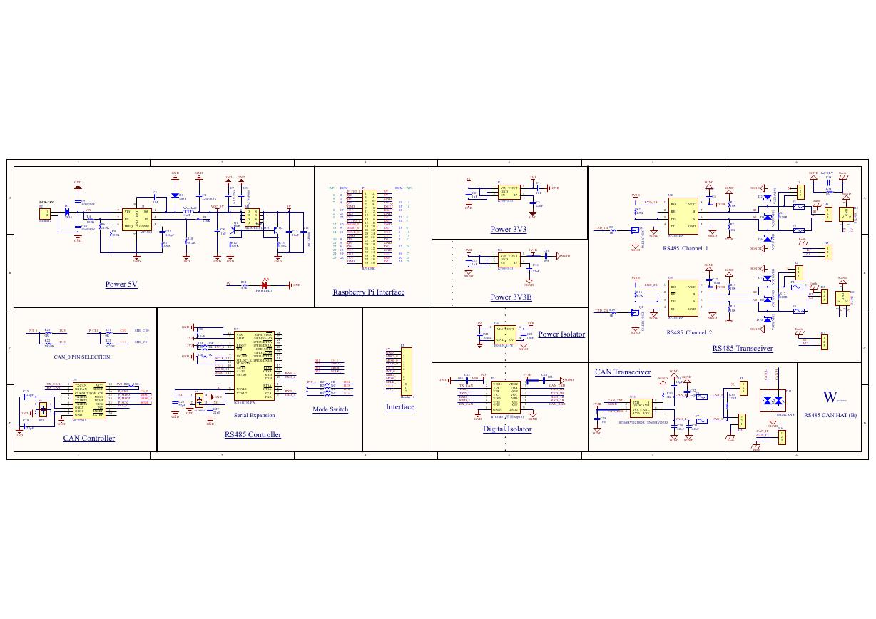 原理图(RS485-CAN-HAT-B-schematic).pdf
 File:SIM7500_SIM7600_SIM7800 Series_SSL_Application Note_V2.00.pdf
 ADS1263(Ads1262).pdf
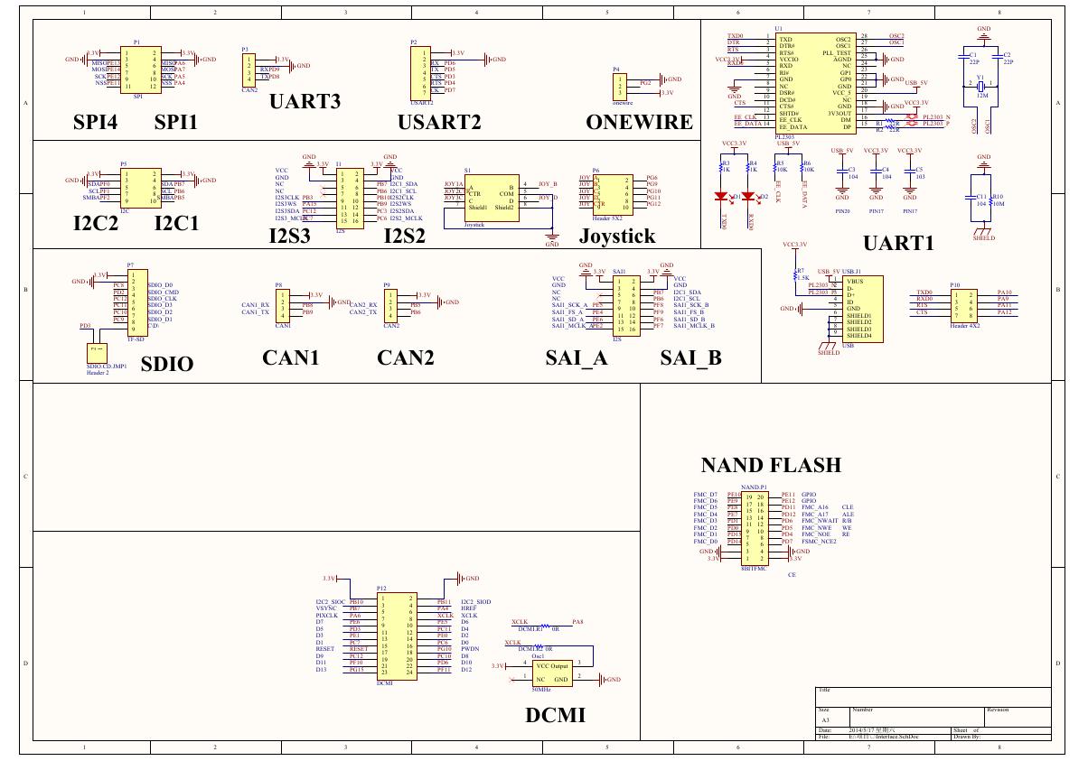 原理图(Open429Z-D-Schematic).pdf
 用户手册(Capacitive_Fingerprint_Reader_User_Manual_CN).pdf
 CY7C68013A(英文版)(CY7C68013A).pdf
 TechnicalReference_Dem.pdf