XAPP951 (v1.3) September 23, 2010
Configuring Xilinx FPGAs with
SPI Serial Flash
Author: Stephanie Tapp
Application Note: Spartan-3E and Virtex-5 FPGAs
Summary
Introduction
SPI Basics
This application note discusses the Serial Peripheral Interface (SPI) configuration mode
introduced in the Virtex®-5 and Spartan®-3E FPGA families. The required connections to
configure the FPGA from an SPI serial flash device are discussed and the configuration flow for
the SPI mode is shown. Special precautions for configuring from an SPI serial flash are given,
and the ISE® Design Suite iMPACT direct SPI programming solution is described.
Note: The ISE Suite iMPACT tool version 11.4 is the last supported release for direct in-system SPI
programming and is captured in this application note. For new designs, the iMPACT indirect in-system SPI
programming solution is recommended. This solution uses a single JTAG connection to both configure the
FPGA and indirectly program the flash. For additional information see Introduction to Indirect
Programming — SPI or BPI Flash Memory in the iMPACT Help at http://www.xilinx.com/support/
documentation/sw_manuals/xilinx11/isehelp_start.htm.
The principles described in this application note apply to the external SPI flash configuration
mode of the Extended Spartan-3A family with few differences. See UG332,
Spartan-3 Generation Configuration User Guide for the unique details and requirements of the
Extended Spartan-3A family's SPI configuration mode.
Xilinx FPGAs are CMOS configurable latch (CCL) based and must be configured at power-up.
Traditionally, Xilinx FPGA configuration is accomplished via the IEEE Std 1149.1 (JTAG)
interface, a microprocessor, or the Xilinx PROMs (Platform Flash PROMs). In addition to these
traditional methods, a direct configuration interface to SPI serial flash is now available.
The direct configuration interface for SPI serial flash memories in the Virtex-5 and Spartan-3E
FPGAs broadens the available configuration solutions for Xilinx designers and is the focus of
this application note. SPI serial flash memories are popular because they can be easily
accessed post-configuration, offering random-access, non-volatile data storage to the FPGA.
Systems with SPI serial flash memory already onboard can also benefit from having the option
to configure the FPGA from the same memory device.
The SPI protocol does have a few variations among vendors. Variations among some vendors
are highlighted along with the connections required between the FPGA and SPI serial flash
memory for configuration. The ISE software tools for SPI-formatted PROM file creation and
programming during prototyping for select vendors are shown. SPI serial flash memories are
not supplied by Xilinx and must be purchased from third-party vendors such as Numonyx.
SPI serial flash memories use the Serial Peripheral Interface (SPI), a four-wire, synchronous
serial data bus. This serial data link was pioneered as a serial communication interface
between a microcontroller and its peripherals and is a popular interface in embedded and
consumer markets. This interface can now also be used to configure Xilinx FPGAs.
An SPI system typically consists of a master device and a slave device (Figure 1). When using
this four-signal interface to configure a Xilinx FPGA from an SPI serial flash, the FPGA is the
master device and the SPI serial flash is the slave device.
© Copyright 2006–2010 Xilinx, Inc. XILINX, the Xilinx logo, Virtex, Spartan, ISE, and other designated brands included herein are trademarks of Xilinx in the United States and
other countries. All other trademarks are the property of their respective owners.
XAPP951 (v1.3) September 23, 2010
www.xilinx.com
1
�
SPI Basics
X-Ref Target - Figure 1
Xilinx FPGA
Master
Device
SCK
MOSI
MISO
SS
SPI Serial
Flash
Slave
Device
Figure 1: Basic Block Diagram for SPI Configuration Mode
X951_01_1115006
The master FPGA device controls the timing via the SCK clock signal. Data is clocked out of the
FPGA master and into the SPI serial flash slave on the MOSI signal after the select signal SS
goes Low. During the same clock cycle, data is clocked out of the SPI serial flash slave and into
the FPGA master using the MISO signal. Data is clocked out of each device on one edge and
clocked into each device on the next opposite edge in the period.
In addition to the four-signal interface, each SPI serial flash vendor has unique control signals,
such as write protect or hold, that need to be controlled appropriately during programming and
configuration (refer to the appropriate vendor’s SPI serial flash memory data sheet for
additional details on the specific control signals).
A cross reference for the FPGA to SPI interface connections is provided in Table 1.
Table 1: SPI Serial Flash Interface Connections and Pin Naming
SPI Signals
SPI Serial
Flash Pins(1)
FPGA Connection
(Spartan-3E/Virtex-5 FPGAs)
General SPI Signals
Signal Description
MOSI
MISO
SS
SCK
D
Q
S
C
MOSI
DIN/D_IN
CSO_B/FCS_B(2)
Master Out Slave In is used by the master to specify the
instruction to execute or to send data to the slave device.
Master In Slave Out is used by the master to collect data
transferred from the slave device.
Slave Select, active-Low signal; when driven High this
signal is used to deselect the slave device and put MISO
at high impedance.
CCLK
Serial Clock provides the timing for the serial interface.
Additional Vendor-Specific SPI Control Signals
Write
Protect
W
Hold
HOLD
Not required for FPGA configuration,
but must be High to program or
erase SPI serial flash. Optional
connection to FPGA user I/O.
Not required for FPGA configuration,
but must be High during FPGA
configuration and SPI erase or
program. Optional connection to
FPGA user I/O.
Write Protect protects select areas of memory against
program or erase instructions.
Hold is used to pause any serial communications with
the device without deselecting the device.
Notes:
1. General SPI serial flash pin names are listed in this table with the most common vendor pin names. The subset of SPI control signals used
by each vendor can vary. Refer to the vendor data sheet for specific pin information and descriptions.
The CSO_B signal is used on Spartan-3E FPGAs and the FCS_B signal is used on the Virtex-5 FPGAs to interface to the SPI serial flash
for configuration. On Virtex-5 FPGAs, the CSO_B signal does not control the chip select on the SPI serial flash but is instead used for
advanced daisy-chains.
2.
XAPP951 (v1.3) September 23, 2010
www.xilinx.com
2
�
Configuring FPGAs from SPI Serial Flash
Configuring
FPGAs from SPI
Serial Flash
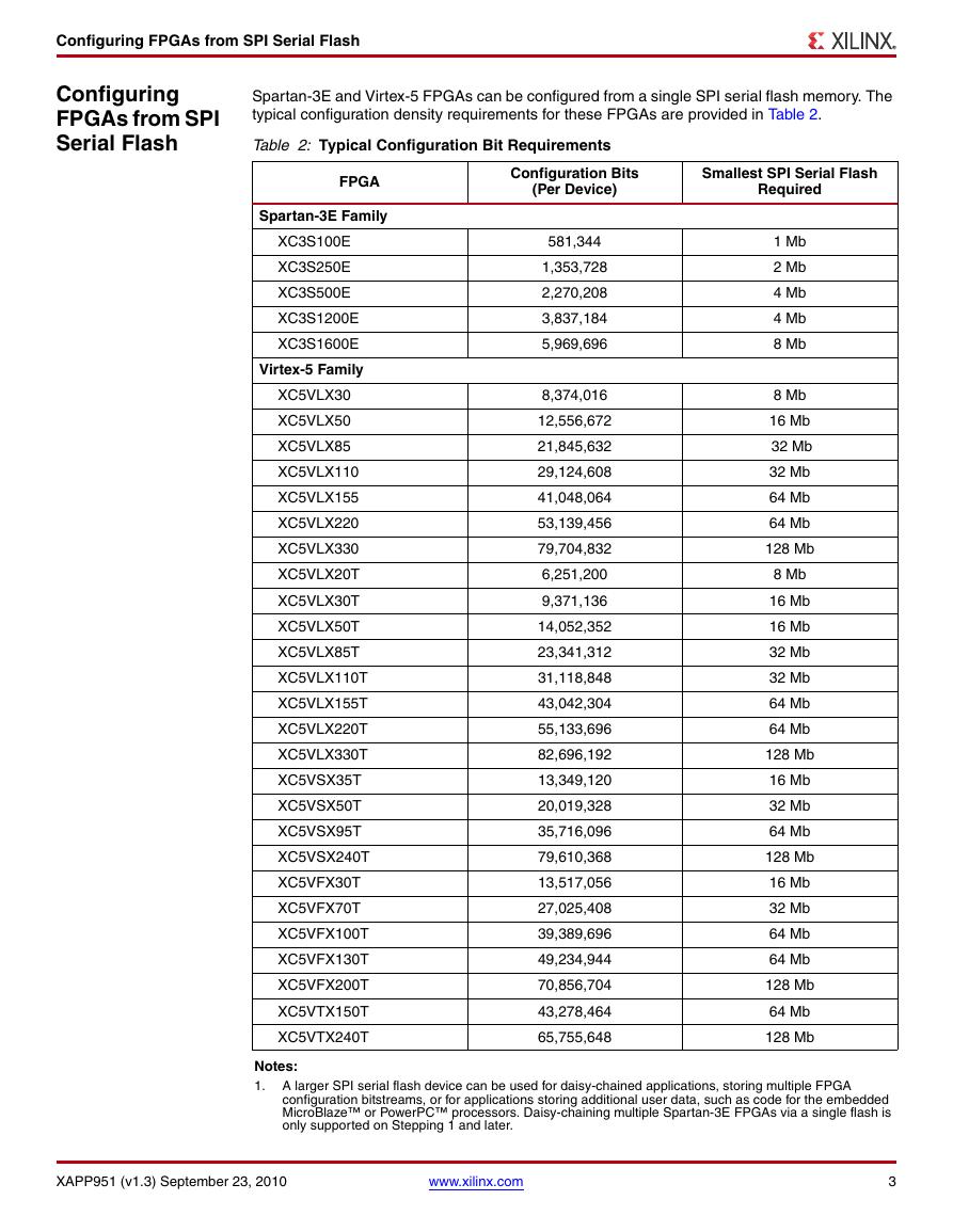
Spartan-3E and Virtex-5 FPGAs can be configured from a single SPI serial flash memory. The
typical configuration density requirements for these FPGAs are provided in Table 2.
Table 2: Typical Configuration Bit Requirements
FPGA
Spartan-3E Family
XC3S100E
XC3S250E
XC3S500E
XC3S1200E
XC3S1600E
Virtex-5 Family
XC5VLX30
XC5VLX50
XC5VLX85
XC5VLX110
XC5VLX155
XC5VLX220
XC5VLX330
XC5VLX20T
XC5VLX30T
XC5VLX50T
XC5VLX85T
XC5VLX110T
XC5VLX155T
XC5VLX220T
XC5VLX330T
XC5VSX35T
XC5VSX50T
XC5VSX95T
XC5VSX240T
XC5VFX30T
XC5VFX70T
XC5VFX100T
XC5VFX130T
XC5VFX200T
XC5VTX150T
XC5VTX240T
Configuration Bits
(Per Device)
Smallest SPI Serial Flash
Required
581,344
1,353,728
2,270,208
3,837,184
5,969,696
8,374,016
12,556,672
21,845,632
29,124,608
41,048,064
53,139,456
79,704,832
6,251,200
9,371,136
14,052,352
23,341,312
31,118,848
43,042,304
55,133,696
82,696,192
13,349,120
20,019,328
35,716,096
79,610,368
13,517,056
27,025,408
39,389,696
49,234,944
70,856,704
43,278,464
65,755,648
1 Mb
2 Mb
4 Mb
4 Mb
8 Mb
8 Mb
16 Mb
32 Mb
32 Mb
64 Mb
64 Mb
128 Mb
8 Mb
16 Mb
16 Mb
32 Mb
32 Mb
64 Mb
64 Mb
128 Mb
16 Mb
32 Mb
64 Mb
128 Mb
16 Mb
32 Mb
64 Mb
64 Mb
128 Mb
64 Mb
128 Mb
Notes:
1. A larger SPI serial flash device can be used for daisy-chained applications, storing multiple FPGA
configuration bitstreams, or for applications storing additional user data, such as code for the embedded
MicroBlaze™ or PowerPC™ processors. Daisy-chaining multiple Spartan-3E FPGAs via a single flash is
only supported on Stepping 1 and later.
XAPP951 (v1.3) September 23, 2010
www.xilinx.com
3
�
Configuring FPGAs from SPI Serial Flash
A detailed SPI configuration setup is shown in Figure 2, page 5, where the Virtex-5 FPGA is the
master and the Numonyx SPI serial flash is the slave. The configuration connections from the
SPI serial flash to the FPGA are highlighted in this diagram. For information on the
programming and configuration headers used by the Xilinx cables, refer to Hardware and
Connections for SPI Programming.
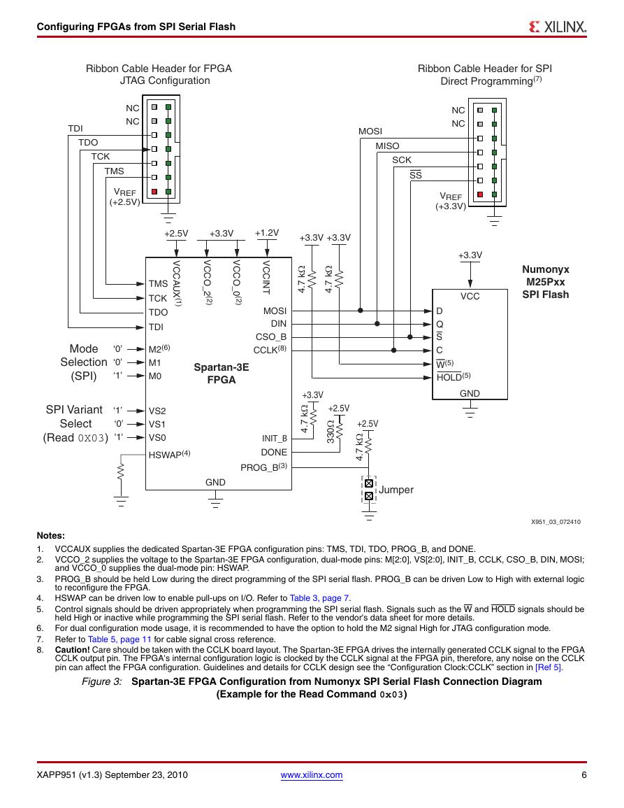
A detailed SPI configuration setup is shown in Figure 3, page 6, where the Spartan-3E FPGA
is the master and the Numonyx SPI serial flash is the slave. The configuration connections from
the SPI serial flash to the FPGA are highlighted in the diagram. For information on the
programming and configuration headers used by the Xilinx cables, refer to Hardware and
Connections for SPI Programming.
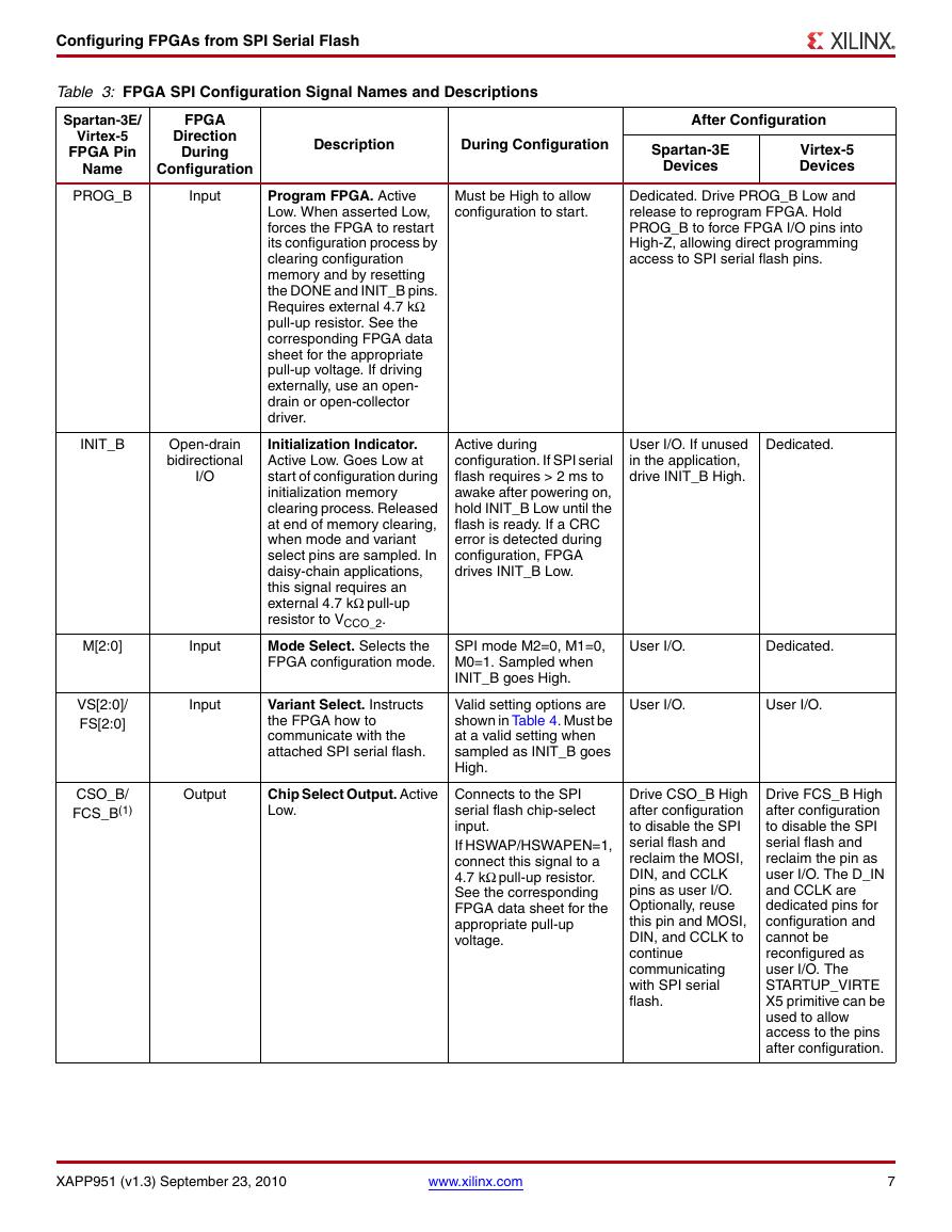
In addition to the SPI serial flash interface signals discussed in SPI Basics, page 1, there are
additional FPGA configuration signals that can influence the successful start and stop of data
transfer. These FPGA signals and their descriptions are listed in Table 3, page 7 and are shown
in Figure 2 and Figure 3.
XAPP951 (v1.3) September 23, 2010
www.xilinx.com
4
�
Configuring FPGAs from SPI Serial Flash
X-Ref Target - Figure 2
Ribbon Cable Header for FPGA
JTAG Configuration
NC
NC
TDI
TDO
TCK
TMS
VREF
(+3.3V)
+2.5V
+3.3V
+1.0V
+3.3V
+3.3V
MOSI
MISO
SCK
SS
Ribbon Cable Header for SPI
Direct Programming(6)
NC
NC
VREF
(+3.3V)
+3.3V
VCC
D
Q
S
C
W(5)
HOLD(5)
GND
Numonyx
M25Pxx
SPI Flash
Mode
Selection
(SPI)
SPI Variant
Select
(Read 0X03)
‘0’
‘0’
‘1’
‘1’
‘0’
'1'
V
C
C
A
U
X
(
1
)
V
C
C
O
_
2
V
C
C
_
C
O
N
F
G
(
2
)
I
Virtex-5
FPGA
TMS
TCK
TDO
TDI
M2
M1
M0
V
C
C
N
T
I
Ω
k
7
.
4
Ω
k
7
.
4
MOSI
D_IN
FCS_B
CCLK(7)
FS2
FS1
FS0
HSWAPEN(4)
INIT_B
DONE
PROG_B(3)
GND
+3.3V
Ω
k
7
.
4
+3.3V
Ω
0
3
3
+3.3V
Ω
k
7
.
4
Jumper
X951_02_072410
Notes:
1. VCCO_2 supplies the SPI configuration dual-mode pins: MOSI, FCS_B, and FS[2:0]
2. VCC_CONFIG (Vcco_0) is the configuration output supply voltage and supplies the dedicated configuration pins: TMS, TCK, TDO, TDI,
M[2:0], HSWAPEN, PROG_B, DONE, INIT_B, CCLK, D_IN.
3. PROG_B should be held Low during the direct programming of the SPI serial flash. PROG_B can be driven Low to High with external logic
to reconfigure the FPGA.
4. HSWAPEN can be driven Low to enable pull-ups on I/O. Refer to Table 3, page 7 and [Ref 2] for details and options on this pin.
5. Control signals should be driven appropriately when programming the SPI serial flash. Signals such as the W and HOLD signals should be
held High or inactive while programming the SPI serial flash. Refer to the vendor's data sheet for more details.
6. Refer to Table 5, page 11 for cable signal cross reference.
7. Caution! Care should be taken with the CCLK board layout. The Virtex-5 FPGA drives the internally generated CCLK signal to the FPGA
CCLK output pin. The FPGA's internal configuration logic is clocked by the CCLK signal at the FPGA pin, therefore, any noise on the CCLK
pin can affect the FPGA configuration. Guidelines and details for CCLK design see the “Board Layout for Configuration Clock (CCLK)” section
in [Ref 3].
Figure 2: Virtex-5 FPGA Configuration from Numonyx SPI Serial Flash Connection Diagram
(Example for the Read Command 0x03)
XAPP951 (v1.3) September 23, 2010
www.xilinx.com
5
�
Configuring FPGAs from SPI Serial Flash
X-Ref Target - Figure 3
Ribbon Cable Header for FPGA
JTAG Configuration
NC
NC
TDI
TDO
TCK
TMS
VREF
(+2.5V)
MOSI
MISO
SCK
SS
Ribbon Cable Header for SPI
Direct Programming(7)
NC
NC
VREF
(+3.3V)
+3.3V
VCC
D
Q
S
C
W(5)
HOLD(5)
GND
Numonyx
M25Pxx
SPI Flash
+2.5V
+3.3V
+1.2V
+3.3V
+3.3V
V
C
C
A
U
X
(
1
)
V
C
C
O
_
2
(
2
)
V
C
C
O
_
0
(
2
)
V
C
C
N
T
I
Ω
k
7
4
.
Ω
k
7
.
4
MOSI
DIN
CSO_B
CCLK(8)
Spartan-3E
FPGA
TMS
TCK
TDO
TDI
M2(6)
M1
M0
VS2
VS1
VS0
HSWAP(4)
INIT_B
DONE
PROG_B(3)
GND
+3.3V
Ω
k
7
4
.
+2.5V
Ω
0
3
3
+2.5V
Ω
k
7
4
.
Jumper
Mode
Selection
(SPI)
SPI Variant
Select
(Read 0X03)
‘0’
‘0’
‘1’
‘1’
‘0’
'1'
Notes:
1. VCCAUX supplies the dedicated Spartan-3E FPGA configuration pins: TMS, TDI, TDO, PROG_B, and DONE.
2. VCCO_2 supplies the voltage to the Spartan-3E FPGA configuration, dual-mode pins: M[2:0], VS[2:0], INIT_B, CCLK, CSO_B, DIN, MOSI;
and VCCO_0 supplies the dual-mode pin: HSWAP.
3. PROG_B should be held Low during the direct programming of the SPI serial flash. PROG_B can be driven Low to High with external logic
to reconfigure the FPGA.
X951_03_072410
4. HSWAP can be driven low to enable pull-ups on I/O. Refer to Table 3, page 7.
5. Control signals should be driven appropriately when programming the SPI serial flash. Signals such as the W and HOLD signals should be
held High or inactive while programming the SPI serial flash. Refer to the vendor's data sheet for more details.
For dual configuration mode usage, it is recommended to have the option to hold the M2 signal High for JTAG configuration mode.
6.
7. Refer to Table 5, page 11 for cable signal cross reference.
8. Caution! Care should be taken with the CCLK board layout. The Spartan-3E FPGA drives the internally generated CCLK signal to the FPGA
CCLK output pin. The FPGA's internal configuration logic is clocked by the CCLK signal at the FPGA pin, therefore, any noise on the CCLK
pin can affect the FPGA configuration. Guidelines and details for CCLK design see the “Configuration Clock:CCLK” section in [Ref 5].
Figure 3: Spartan-3E FPGA Configuration from Numonyx SPI Serial Flash Connection Diagram
(Example for the Read Command 0x03)
XAPP951 (v1.3) September 23, 2010
www.xilinx.com
6
�
Configuring FPGAs from SPI Serial Flash
Table 3: FPGA SPI Configuration Signal Names and Descriptions
Spartan-3E/
Virtex-5
FPGA Pin
Name
FPGA
Direction
During
Configuration
Description
During Configuration
PROG_B
Input
INIT_B
Open-drain
bidirectional
I/O
M[2:0]
Input
VS[2:0]/
FS[2:0]
Input
Program FPGA. Active
Low. When asserted Low,
forces the FPGA to restart
its configuration process by
clearing configuration
memory and by resetting
the DONE and INIT_B pins.
Requires external 4.7 kΩ
pull-up resistor. See the
corresponding FPGA data
sheet for the appropriate
pull-up voltage. If driving
externally, use an open-
drain or open-collector
driver.
Initialization Indicator.
Active Low. Goes Low at
start of configuration during
initialization memory
clearing process. Released
at end of memory clearing,
when mode and variant
select pins are sampled. In
daisy-chain applications,
this signal requires an
external 4.7 kΩ pull-up
resistor to VCCO_2.
Mode Select. Selects the
FPGA configuration mode.
Variant Select. Instructs
the FPGA how to
communicate with the
attached SPI serial flash.
CSO_B/
FCS_B(1)
Output
Chip Select Output. Active
Low.
Must be High to allow
configuration to start.
Active during
configuration. If SPI serial
flash requires > 2 ms to
awake after powering on,
hold INIT_B Low until the
flash is ready. If a CRC
error is detected during
configuration, FPGA
drives INIT_B Low.
SPI mode M2=0, M1=0,
M0=1. Sampled when
INIT_B goes High.
Valid setting options are
shown in Table 4. Must be
at a valid setting when
sampled as INIT_B goes
High.
Connects to the SPI
serial flash chip-select
input.
If HSWAP/HSWAPEN=1,
connect this signal to a
4.7 kΩ pull-up resistor.
See the corresponding
FPGA data sheet for the
appropriate pull-up
voltage.
After Configuration
Spartan-3E
Devices
Virtex-5
Devices
Dedicated. Drive PROG_B Low and
release to reprogram FPGA. Hold
PROG_B to force FPGA I/O pins into
High-Z, allowing direct programming
access to SPI serial flash pins.
User I/O. If unused
in the application,
drive INIT_B High.
Dedicated.
User I/O.
Dedicated.
User I/O.
User I/O.
Drive CSO_B High
after configuration
to disable the SPI
serial flash and
reclaim the MOSI,
DIN, and CCLK
pins as user I/O.
Optionally, reuse
this pin and MOSI,
DIN, and CCLK to
continue
communicating
with SPI serial
flash.
Drive FCS_B High
after configuration
to disable the SPI
serial flash and
reclaim the pin as
user I/O. The D_IN
and CCLK are
dedicated pins for
configuration and
cannot be
reconfigured as
user I/O. The
STARTUP_VIRTE
X5 primitive can be
used to allow
access to the pins
after configuration.
XAPP951 (v1.3) September 23, 2010
www.xilinx.com
7
�
Configuring FPGAs from SPI Serial Flash
Table 3: FPGA SPI Configuration Signal Names and Descriptions (Cont’d)
Spartan-3E/
Virtex-5
FPGA Pin
Name
FPGA
Direction
During
Configuration
Description
During Configuration
After Configuration
Spartan-3E
Devices
Virtex-5
Devices
CCLK
Output
Configuration Clock.
Generated by FPGA
internal oscillator.
Frequency controlled by
ConfigRate bitstream
generator option. If CCLK
PCB trace is long or has
multiple connections,
terminate this output to
maintain signal integrity.
MOSI
Output
Serial Data Output.
DIN/
D_IN
DONE
Input
Serial Data Input.
Open-drain
bidirectional
I/O
FPGA Configuration
Done. Low during
configuration. Goes High
when FPGA successfully
completes configuration.
Requires external 330Ω
pull-up resistor. See the
corresponding FPGA data
sheet for the appropriate
pull-up voltage.
DOUT
Output
Serial Data Output.
HSWAP/
HSWAPEN
Input
User I/O Pull-Up Control.
When Low during
configuration, enables pull-
up resistors in all I/O pins to
respective I/O bank VCCO
input:
0: Pull-ups during
configuration
1: No pull-ups
Drives the SPI serial flash
clock input.
User I/O.
Dedicated.
FPGA sends SPI serial
flash read commands
and starting address to
the flash serial data input.
FPGA receives serial
data from flash serial data
output.
User I/O.
User I/O.
User I/O.
Dedicated.
Low indicates that the
FPGA is not yet
configured.
Pulled High via external pull-up. When
High, indicates that the FPGA
successfully configured.
Actively drives. Not used
in single-FPGA
configuration. In a daisy-
chain configuration, this
pin connects to DIN/D_IN
input of the next FPGA in
the chain. The
downstream FPGA is
now in Slave Serial mode.
Drive at valid logic level
throughout configuration.
User I/O.
Dedicated.
User I/O.
Dedicated.
Notes:
1.
For SPI ISP Programming, CSO_B is used for Spartan-3E FPGAs and FCS_B is used on Virtex-5 FPGAs. On Virtex-5 FPGAs, the CSO_B
signal is used for the advanced daisy-chaining feature and not for SPI ISP programming. Refer to the FPGA data sheets or FPGA
configuration user guides for additional information.
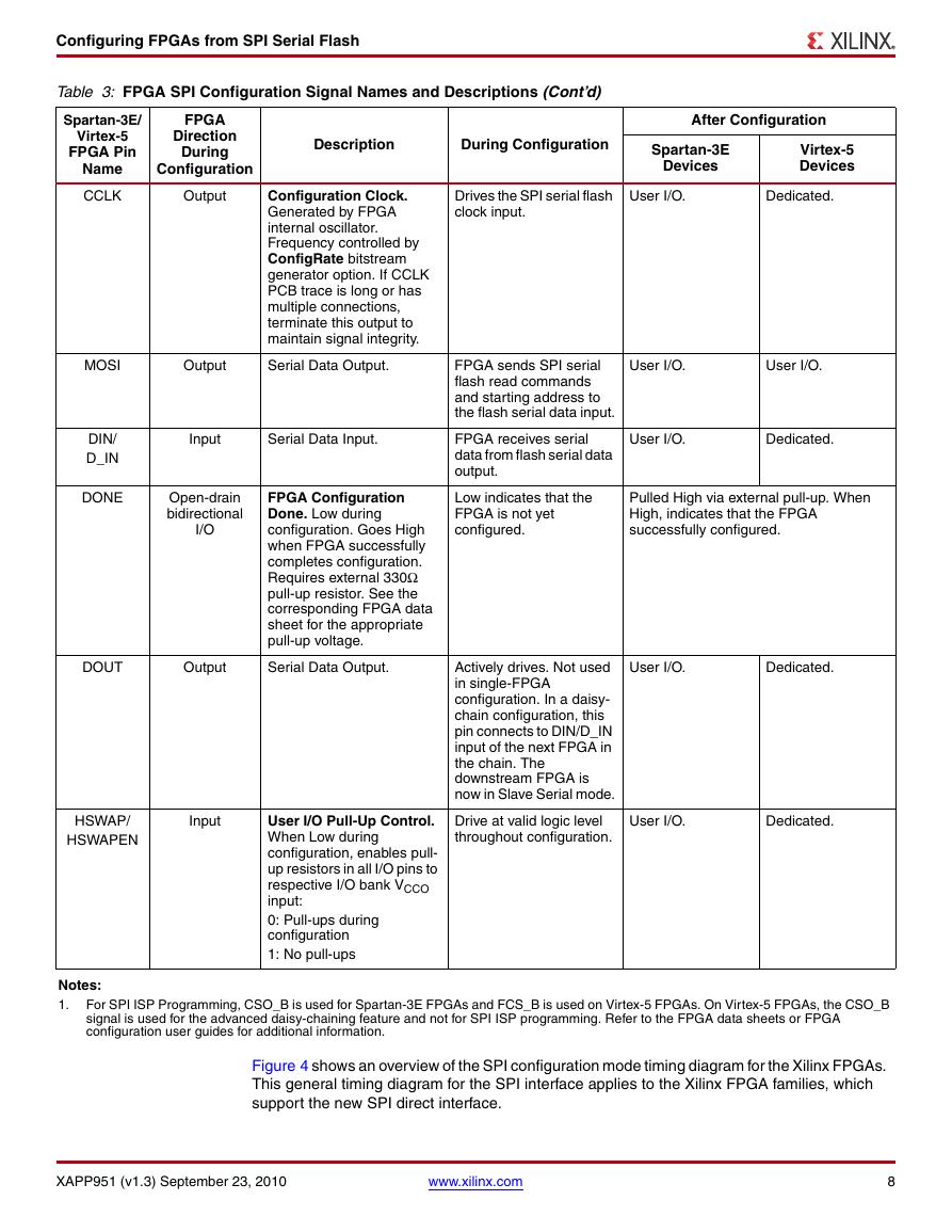
Figure 4 shows an overview of the SPI configuration mode timing diagram for the Xilinx FPGAs.
This general timing diagram for the SPI interface applies to the Xilinx FPGA families, which
support the new SPI direct interface.
XAPP951 (v1.3) September 23, 2010
www.xilinx.com
8
�





 V2版本原理图(Capacitive-Fingerprint-Reader-Schematic_V2).pdf
 摄像头工作原理.doc
 VL53L0X简要说明(En.FLVL53L00216).pdf
 原理图(DVK720-Schematic).pdf
 原理图(Pico-Clock-Green-Schdoc).pdf
 原理图(RS485-CAN-HAT-B-schematic).pdf
 File:SIM7500_SIM7600_SIM7800 Series_SSL_Application Note_V2.00.pdf
 ADS1263(Ads1262).pdf
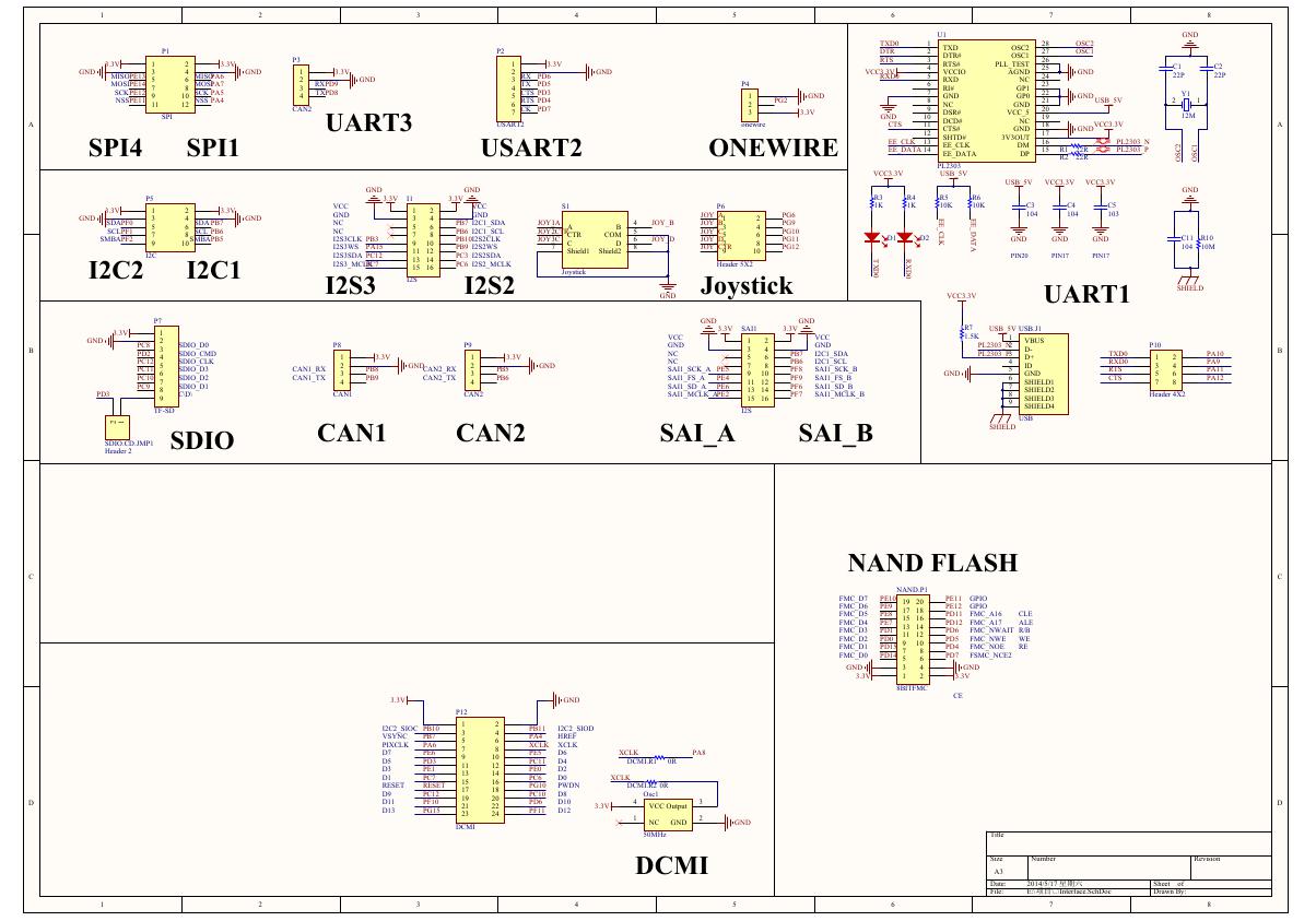 原理图(Open429Z-D-Schematic).pdf
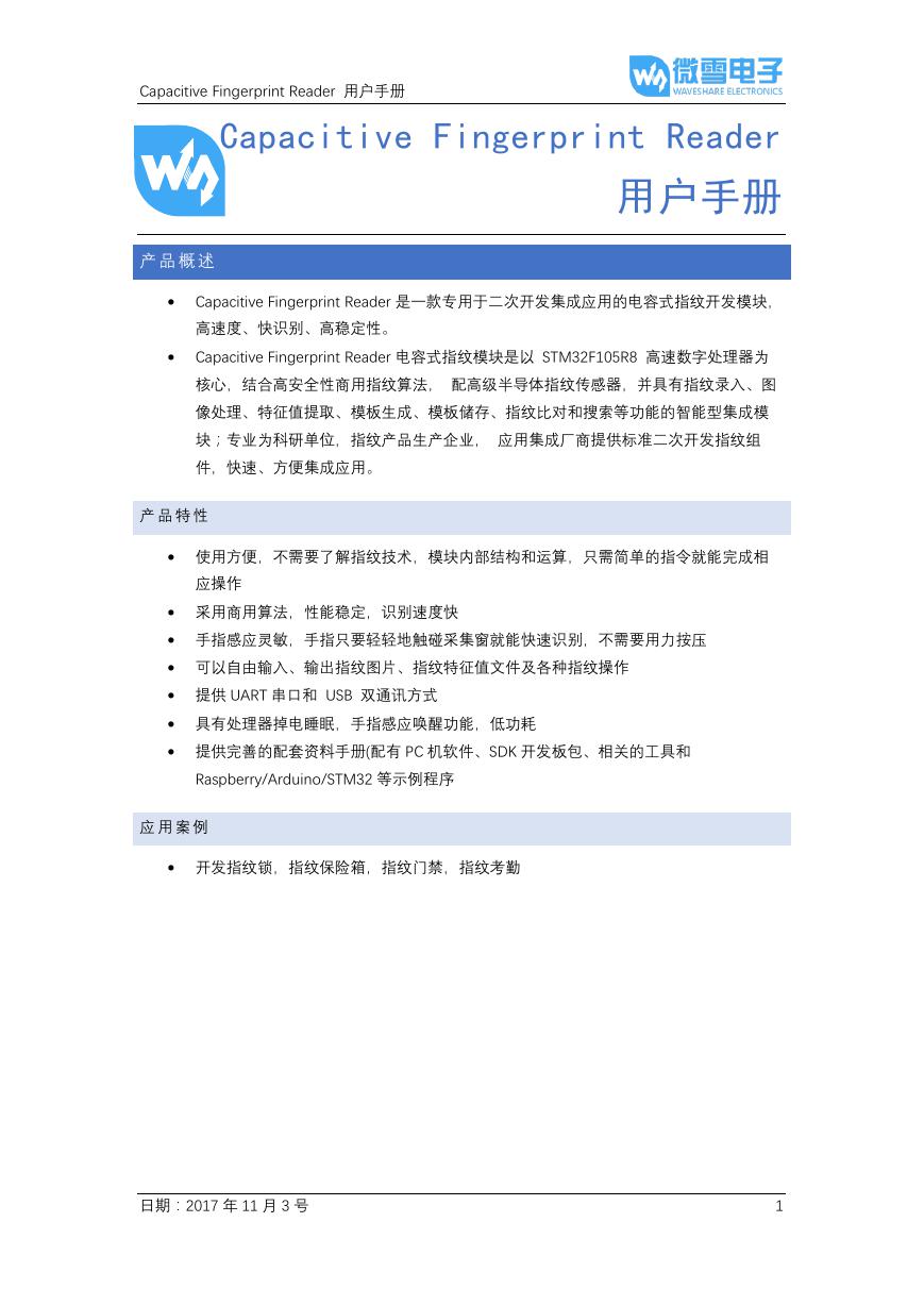 用户手册(Capacitive_Fingerprint_Reader_User_Manual_CN).pdf
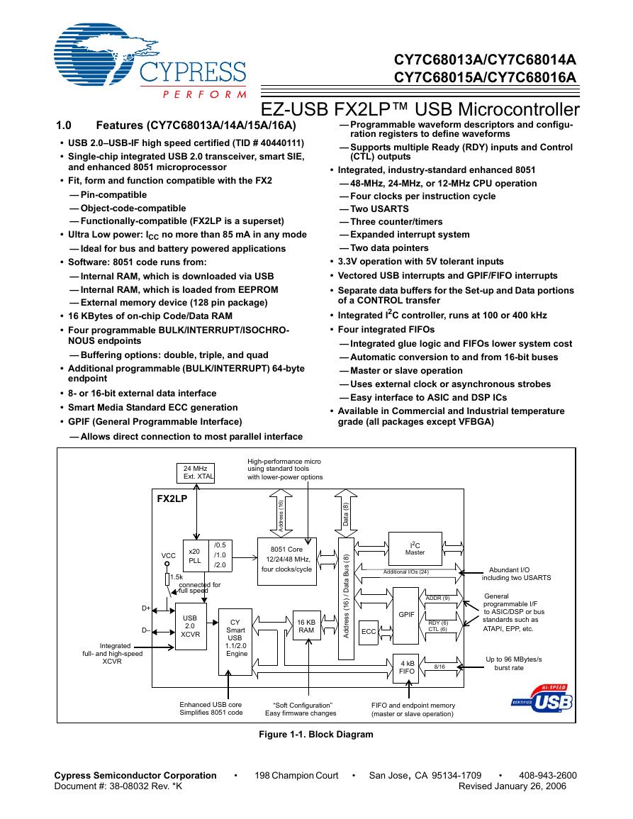 CY7C68013A(英文版)(CY7C68013A).pdf
 TechnicalReference_Dem.pdf