CH9120 Datasheet
1
Network and UART Transparent Transmission Chip CH9120
Datasheet
Version: 1B
1. Overview
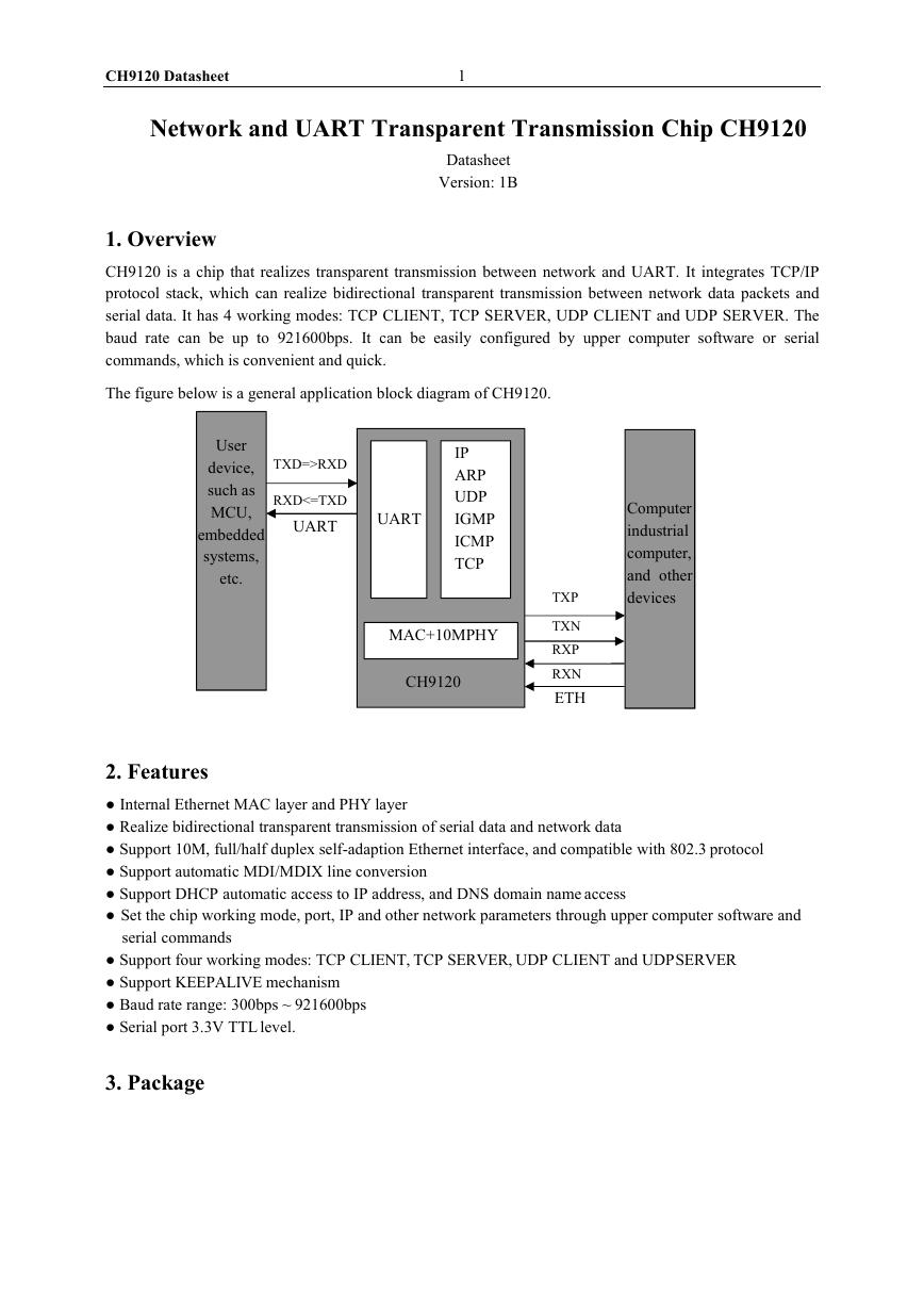
CH9120 is a chip that realizes transparent transmission between network and UART. It integrates TCP/IP
protocol stack, which can realize bidirectional transparent transmission between network data packets and
serial data. It has 4 working modes: TCP CLIENT, TCP SERVER, UDP CLIENT and UDP SERVER. The
baud rate can be up to 921600bps. It can be easily configured by upper computer software or serial
commands, which is convenient and quick.
The figure below is a general application block diagram of CH9120.
User
device,
such as
MCU,
embedded
systems,
etc.
TXD=>RXD
RXD<=TXD
UART
UART
IP
ARP
UDP
IGMP
ICMP
TCP
MAC+10MPHY
CH9120
Computer
industrial
computer,
and other
devices
TXP
TXN
RXP
RXN
ETH
2. Features
● Internal Ethernet MAC layer and PHY layer
● Realize bidirectional transparent transmission of serial data and network data
● Support 10M, full/half duplex self-adaption Ethernet interface, and compatible with 802.3 protocol
● Support automatic MDI/MDIX line conversion
● Support DHCP automatic access to IP address, and DNS domain name access
● Set the chip working mode, port, IP and other network parameters through upper computer software and
serial commands
● Support four working modes: TCP CLIENT, TCP SERVER, UDP CLIENT and UDPSERVER
● Support KEEPALIVE mechanism
● Baud rate range: 300bps ~ 921600bps
● Serial port 3.3V TTL level.
3. Package
�
CH9120 Datasheet
2
1
2
0
2
9
1
8
1
7
1
6
1
5
1
C
N
F
E
R
V
I
X
O
X
N
U
R
I
T
S
R
K
N
I
L
22
23
24
25
26
27
28
VCC
CFGEN
NC
RS485DIR
CFG0
RESET
TCPCS
ACT
NC
NC
TXN
TXP
RXN
RXP
14
13
12
11
10
9
8
D
N
G
C
N
C
N
C
C
V
C
C
V
D
D
V
D
X
R
D
X
T
0
1234567
Chip
CH9120
Name
QFN28
Package
Description
QFN package; 28pins; package body 4x4mm
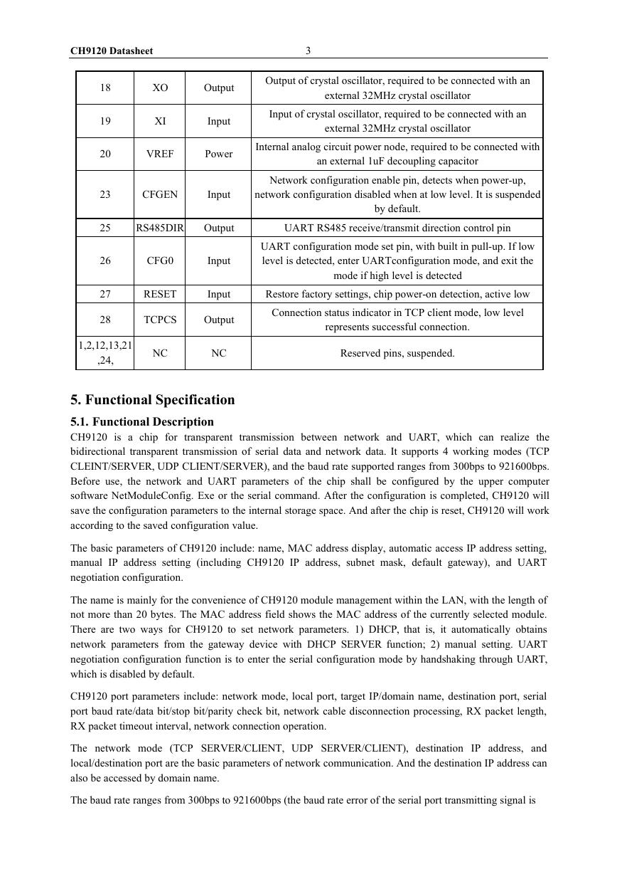
4. Pins
CH9120
Pin No.
0
3,4,22
Pin
Name
GND
VCC
Pin Type
Power
Power
5
6
7
8
9
10
11
14
15
16
17
VDD
Power
RXD
TXD
RXP
RXN
TXP
TXN
ACT
LINK
RSTI
RUN
Input
Output
Ethernet
signal
Ethernet
signal
Ethernet
signal
Ethernet
signal
Output
Output
Input
Output
Pin description
Ground
Internal power supply, required to be externally connected with
a 0.1uF decoupling capacitor
3.3V working voltage input, externally connected with a 2.2UF
decoupling capacitor
UART data input, with built-in pull-up resistor
UART data output, with built-in pull-up resistor
Ethernet RXP signal
Ethernet RXN signal
Ethernet TXP signal
Ethernet TXN signal
Ethernet connection communication indicator LED drive pin
PHY connection indication pin, active low
External reset input, active low
CH9120 running status indication pin, multiplexed as ISP
upgrade pin
�
CH9120 Datasheet
3
18
19
20
23
25
26
27
28
XO
XI
Output
Input
Output of crystal oscillator, required to be connected with an
external 32MHz crystal oscillator
Input of crystal oscillator, required to be connected with an
external 32MHz crystal oscillator
VREF
Power
Internal analog circuit power node, required to be connected with
an external 1uF decoupling capacitor
CFGEN
Input
Network configuration enable pin, detects when power-up,
network configuration disabled when at low level. It is suspended
by default.
RS485DIR
Output
UART RS485 receive/transmit direction control pin
CFG0
RESET
TCPCS
Input
Input
Output
UART configuration mode set pin, with built in pull-up. If low
level is detected, enter UARTconfiguration mode, and exit the
mode if high level is detected
Restore factory settings, chip power-on detection, active low
Connection status indicator in TCP client mode, low level
represents successful connection.
1,2,12,13,21
,24,
NC
NC
Reserved pins, suspended.
5. Functional Specification
5.1. Functional Description
CH9120 is a chip for transparent
transmission between network and UART, which can realize the
bidirectional transparent transmission of serial data and network data. It supports 4 working modes (TCP
CLEINT/SERVER, UDP CLIENT/SERVER), and the baud rate supported ranges from 300bps to 921600bps.
Before use, the network and UART parameters of the chip shall be configured by the upper computer
software NetModuleConfig. Exe or the serial command. After the configuration is completed, CH9120 will
save the configuration parameters to the internal storage space. And after the chip is reset, CH9120 will work
according to the saved configuration value.
The basic parameters of CH9120 include: name, MAC address display, automatic access IP address setting,
manual IP address setting (including CH9120 IP address, subnet mask, default gateway), and UART
negotiation configuration.
The name is mainly for the convenience of CH9120 module management within the LAN, with the length of
not more than 20 bytes. The MAC address field shows the MAC address of the currently selected module.
There are two ways for CH9120 to set network parameters. 1) DHCP, that is, it automatically obtains
network parameters from the gateway device with DHCP SERVER function; 2) manual setting. UART
negotiation configuration function is to enter the serial configuration mode by handshaking through UART,
which is disabled by default.
CH9120 port parameters include: network mode, local port, target IP/domain name, destination port, serial
port baud rate/data bit/stop bit/parity check bit, network cable disconnection processing, RX packet length,
RX packet timeout interval, network connection operation.
The network mode (TCP SERVER/CLIENT, UDP SERVER/CLIENT), destination IP address, and
local/destination port are the basic parameters of network communication. And the destination IP address can
also be accessed by domain name.
The baud rate ranges from 300bps to 921600bps (the baud rate error of the serial port transmitting signal is
�
CH9120 Datasheet
4
less than 0.5%, and the allowable baud rate error of the serial port receiving signal is not less than 2%). It
supports 5/6/7/8 data bits, 1/2 stop bits, odd/even/no parity check, blank 0, and mark 1 check mode.
The network cable disconnection processing means that when the network cable is disconnected, CH9120
actively closes the connection or does not take any action.
The length range of RX packet is 1-512, which means that when the length of CH9120 UART receiving data
reaches the set length, CH9120 will immediately package the serial data and send it out via network. The
timeout time setting range is 0-200, and the timeout unit is about 5ms. For example, when the timeout is 1,
the data length of the serial port receiving buffer does not reach the length of the RX packet, and the serial
port does not receive a new one in more than 5ms, the serial port timeout will occur. After the serial port
timeout occurs, CH9120 will send the data received by the serial port over the network. When the timeout
time is set to 0, the internal hardware timeout mechanism (no new data is received after 4 data times) will be
enabled, which is suitable for occasions where real-time requirements are high and large quantities of data
are sent and received.
Clear serial port buffer setting refers to how the data received by the serial port is processed before the
network connection is established, the data is cleared (discarded) after TCP connection or retained.
5.2. Default Configuration
When CH9120 leaves factory, the network works in TCP CLIENT mode by default. The default parameters
related to the network are as follows:
(1) Device IP: 192.168.1.200
(2) Subnet mask: 255.255.255.0
(3) Default gateway: 192.168.1.1
(4) Module port: 2000
(5) Destination IP: 192.168.1.100
(6) Destination port: 1000
UART related default parameters are:
(1) Baud rate: 9600
(2) Timeout: 0
(3) Data bit: 8. Stop bit: 1. Parity check bit: No
(4) Clear serial port buffer: Never
6. Parameters
6.1. Absolute Maximum Value
Critical value or exceeding the absolute maximum value may cause the chip to work abnormally or even be
damaged.
Name
Parameter description
Min.
Max.
Unit
TA
TS
VDD
VIO
Ambient temperature during
operation
Ambient temperature during storage
VDD=3.3V
Supply voltage (VDD connects to the positive power, GND
to ground)
Voltage on the input or output pins
-40
-55
-0.4
-0.4
85
125
4.0
VDD+0.4
℃
℃
V
V
�
CH9120 Datasheet
5
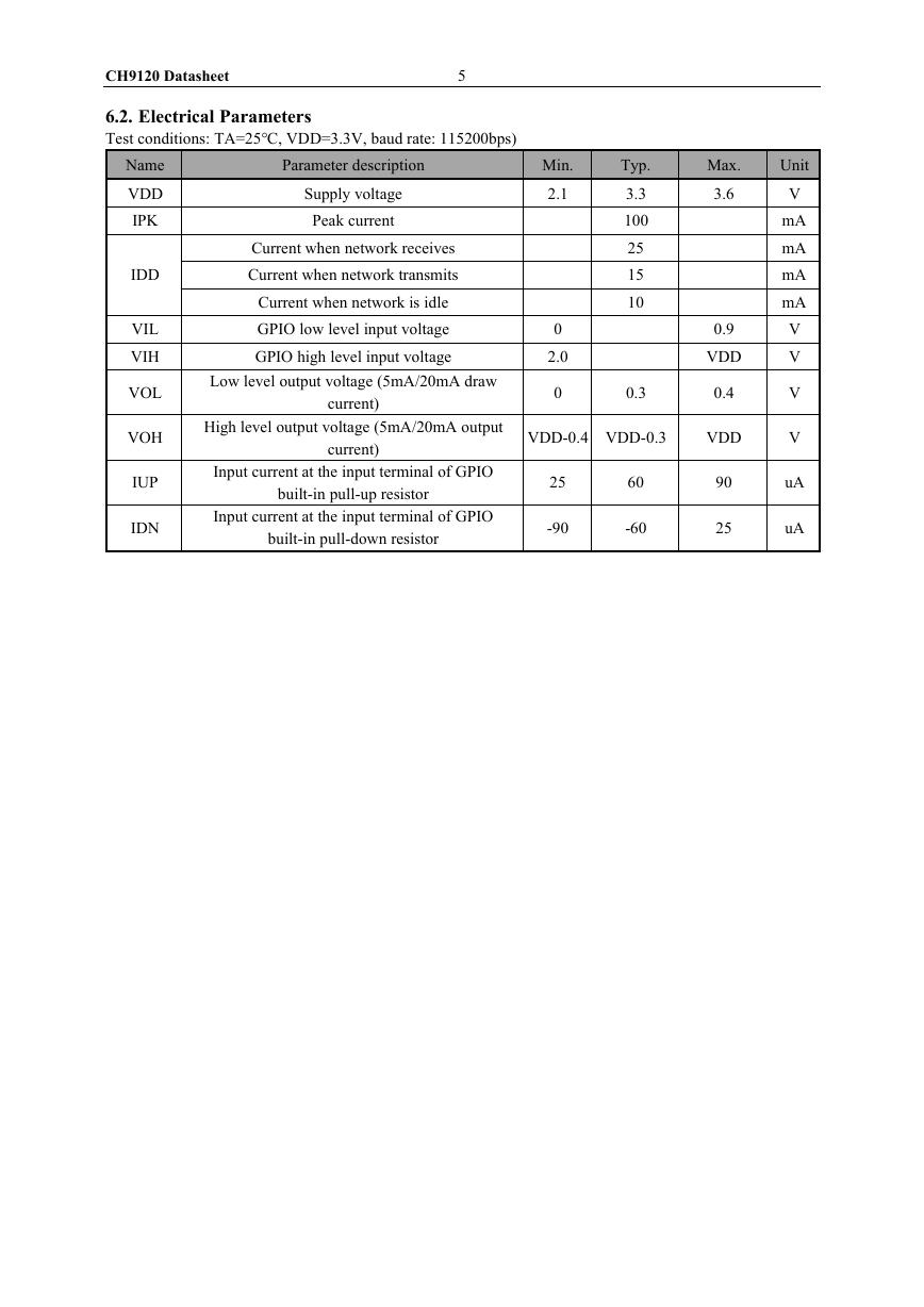
6.2. Electrical Parameters
Test conditions: TA=25℃, VDD=3.3V, baud rate: 115200bps)
Name
VDD
IPK
IDD
VIL
VIH
VOL
VOH
IUP
IDN
Parameter description
Supply voltage
Peak current
Current when network receives
Current when network transmits
Current when network is idle
GPIO low level input voltage
GPIO high level input voltage
Low level output voltage (5mA/20mA draw
current)
High level output voltage (5mA/20mA output
current)
Input current at the input terminal of GPIO
built-in pull-up resistor
Input current at the input terminal of GPIO
built-in pull-down resistor
Min.
2.1
0
2.0
0
Typ.
3.3
100
25
15
10
0.3
VDD-0.4 VDD-0.3
25
-90
60
-60
Max.
3.6
0.9
VDD
0.4
VDD
90
25
Unit
V
mA
mA
mA
mA
V
V
V
V
uA
uA
�




 V2版本原理图(Capacitive-Fingerprint-Reader-Schematic_V2).pdf
 摄像头工作原理.doc
 VL53L0X简要说明(En.FLVL53L00216).pdf
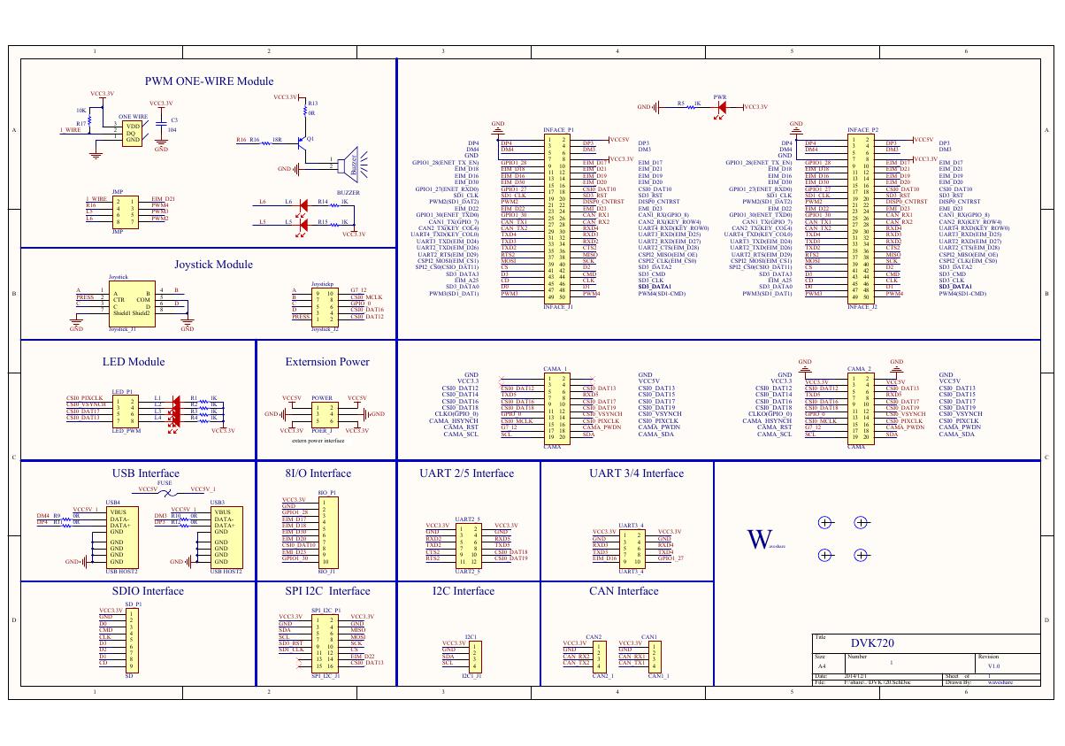 原理图(DVK720-Schematic).pdf
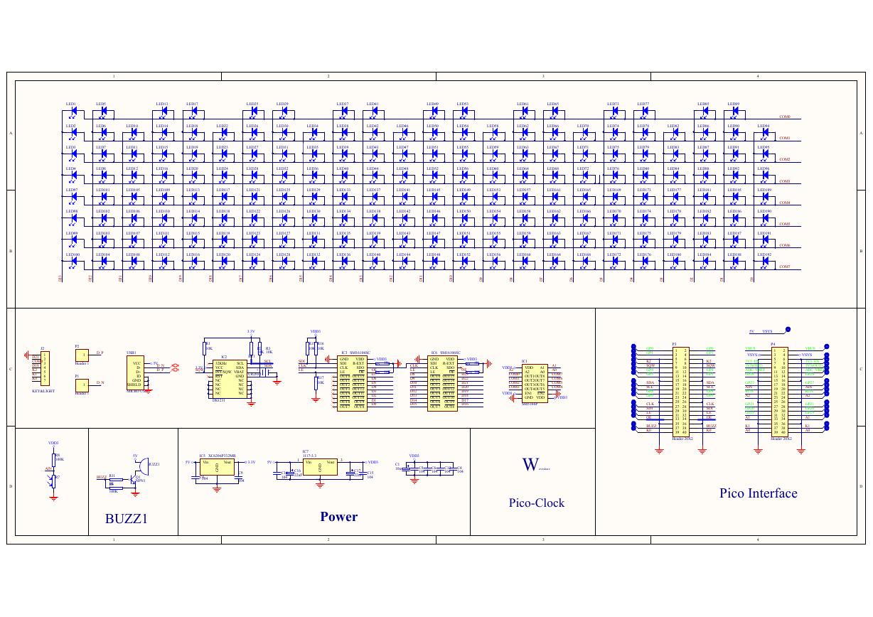 原理图(Pico-Clock-Green-Schdoc).pdf
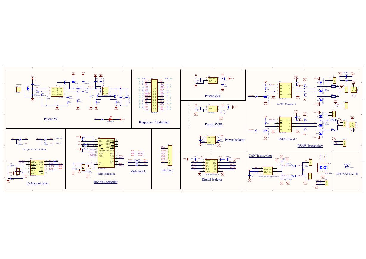 原理图(RS485-CAN-HAT-B-schematic).pdf
 File:SIM7500_SIM7600_SIM7800 Series_SSL_Application Note_V2.00.pdf
 ADS1263(Ads1262).pdf
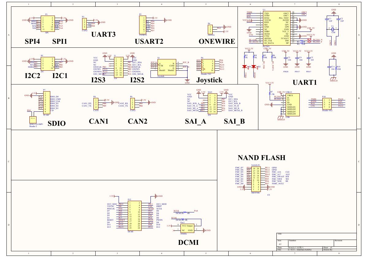 原理图(Open429Z-D-Schematic).pdf
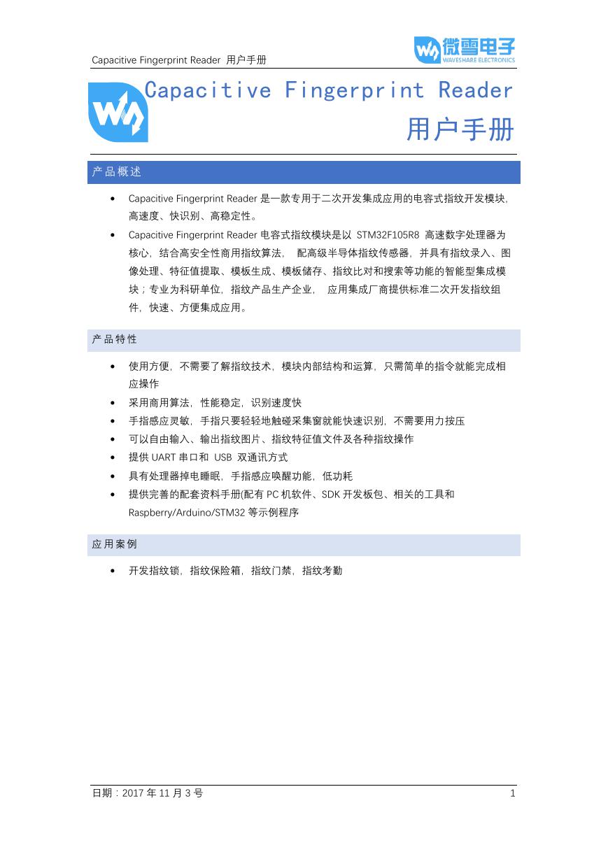 用户手册(Capacitive_Fingerprint_Reader_User_Manual_CN).pdf
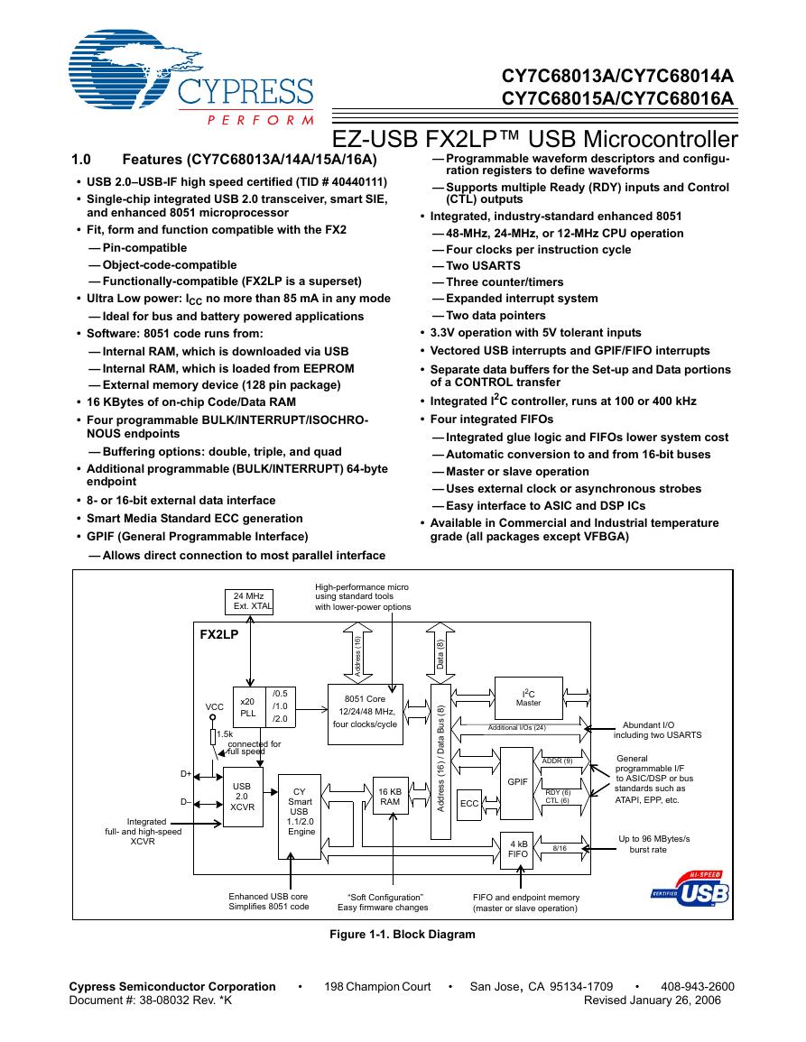 CY7C68013A(英文版)(CY7C68013A).pdf
 TechnicalReference_Dem.pdf