1 Features
1• PWM Microstepping Stepper Motor Driver
– Built-In Microstepping Indexer
– Up to 1/32 Microstepping
• Multiple Decay Modes
– Mixed Decay
– Slow Decay
– Fast Decay
8.2-V to 45-V Operating Supply Voltage Range
2.5-A Maximum Drive Current at 24 V and
TA = 25°C
•
•
Low Current Sleep Mode
• Simple STEP/DIR Interface
•
• Built-In 3.3-V Reference Output
• Small Package and Footprint
• Protection Features
DRV8825
SLVSA73F –APRIL 2010–REVISED JULY 2014
DRV8825 Stepper Motor Controller IC
3 Description
The DRV8825 provides an integrated motor driver
solution for printers, scanners, and other automated
equipment applications. The device has two H-bridge
drivers and a microstepping indexer, and is intended
to drive a bipolar stepper motor. The output driver
block
consists of N-channel power MOSFET’s
configured as full H-bridges to drive the motor
windings. The DRV8825 is capable of driving up to
2.5 A of current from each output (with proper heat
sinking, at 24 V and 25°C).
A simple STEP/DIR interface allows easy interfacing
to controller circuits. Mode pins allow for configuration
of the motor in full-step up to 1/32-step modes. Decay
mode is configurable so that slow decay, fast decay,
or mixed decay can be used. A low-power sleep
mode is provided which shuts down internal circuitry
to achieve very low quiescent current draw. This
sleep mode can be set using a dedicated nSLEEP
pin.
Internal
for
overcurrent, short circuit, under voltage lockout and
over temperature. Fault conditions are indicated via
the nFAULT pin.
shutdown
functions
provided
are
– Overcurrent Protection (OCP)
– Thermal Shutdown (TSD)
– VM Undervoltage Lockout (UVLO)
– Fault Condition Indication Pin (nFAULT)
Device Information(1)
PART NUMBER
BODY SIZE (NOM)
9.70 mm × 6.40 mm
DRV8825
(1) For all available packages, see the orderable addendum at
HTSSOP (28)
PACKAGE
the end of the data sheet.
2 Applications
• Automatic Teller Machines
• Money Handling Machines
• Video Security Cameras
• Printers
• Scanners
• Office Automation Machines
• Gaming Machines
• Factory Automation
• Robotics
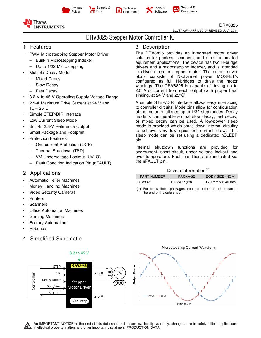
4 Simplified Schematic
Microstepping Current Waveform
1
An IMPORTANT NOTICE at the end of this data sheet addresses availability, warranty, changes, use in safety-critical applications,
intellectual property matters and other important disclaimers. PRODUCTION DATA.
STEPStep SizeDecay Mode8.2 to 45 VControllerM+ -+ -DRV88251/32 µstepStepper Motor Driver2.5 A2.5 ADIRnFAULTProductFolderSample &BuyTechnicalDocumentsTools &SoftwareSupport &Community�
DRV8825
SLVSA73F –APRIL 2010–REVISED JULY 2014
Table of Contents
www.ti.com
1
Features.................................................................. 1
2 Applications ........................................................... 1
3 Description ............................................................. 1
4 Simplified Schematic............................................. 1
5 Revision History..................................................... 2
6 Pin Configuration and Functions ......................... 3
7 Specifications......................................................... 4
7.1 Absolute Maximum Ratings ...................................... 4
7.2 Handling Ratings....................................................... 4
7.3 Recommended Operating Conditions....................... 4
7.4 Thermal Information.................................................. 5
7.5 Electrical Characteristics........................................... 6
7.6 Timing Requirements................................................ 7
7.7 Typical Characteristics.............................................. 8
8 Detailed Description .............................................. 9
8.1 Overview ................................................................... 9
8.2 Functional Block Diagram ....................................... 10
5 Revision History
8.3 Feature Description................................................. 11
8.4 Device Functional Modes........................................ 17
9 Application and Implementation ........................ 18
9.1 Application Information............................................ 18
9.2 Typical Application ................................................. 18
10 Power Supply Recommendations ..................... 21
10.1 Bulk Capacitance .................................................. 21
10.2 Power Supply and Logic Sequencing ................... 21
11 Layout................................................................... 22
11.1 Layout Guidelines ................................................. 22
11.2 Layout Example .................................................... 22
11.3 Thermal Protection................................................ 22
12 Device and Documentation Support ................. 24
12.1 Trademarks ........................................................... 24
12.2 Electrostatic Discharge Caution............................ 24
12.3 Glossary ................................................................ 24
13 Mechanical, Packaging, and Orderable
Information ........................................................... 24
Changes from Revision E (August 2013) to Revision F
Page
• Added new sections and reordered data sheet to fit new TI flow .......................................................................................... 1
• Updated pin descriptions ....................................................................................................................................................... 3
• Added power supply ramp rate and updated ISENSEx pin voltage in Absolute Maximum Ratings ..................................... 4
• Updated VIL voltage minimum and typical in Electrical Characteristics ................................................................................. 6
• Updated IIN and tDEG in Electrical Characteristics .................................................................................................................. 6
2
Submit Documentation Feedback
Copyright © 2010–2014, Texas Instruments Incorporated
Product Folder Links: DRV8825
�
www.ti.com
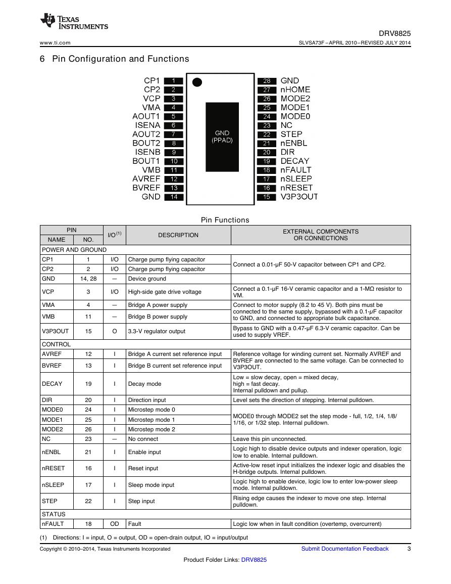
6 Pin Configuration and Functions
DRV8825
SLVSA73F –APRIL 2010–REVISED JULY 2014
PIN
NAME
NO.
I/O(1)
DESCRIPTION
EXTERNAL COMPONENTS
OR CONNECTIONS
Pin Functions
POWER AND GROUND
CP1
CP2
GND
14, 28
1
2
VCP
VMA
VMB
V3P3OUT
CONTROL
AVREF
BVREF
DECAY
DIR
MODE0
MODE1
MODE2
NC
nENBL
nRESET
nSLEEP
STEP
STATUS
nFAULT
3
4
11
15
12
13
19
20
24
25
26
23
21
16
17
22
18
Charge pump flying capacitor
Charge pump flying capacitor
I/O
I/O
— Device ground
I/O
High-side gate drive voltage
— Bridge A power supply
— Bridge B power supply
O
3.3-V regulator output
I
I
I
Bridge A current set reference input
Bridge B current set reference input
Decay mode
Direction input
Microstep mode 0
Microstep mode 1
Microstep mode 2
I
I
I
I
— No connect
I
I
I
I
Enable input
Reset input
Sleep mode input
Step input
Connect a 0.01-μF 50-V capacitor between CP1 and CP2.
Connect a 0.1-μF 16-V ceramic capacitor and a 1-MΩ resistor to
VM.
Connect to motor supply (8.2 to 45 V). Both pins must be
connected to the same supply, bypassed with a 0.1-µF capacitor
to GND, and connected to appropriate bulk capacitance.
Bypass to GND with a 0.47-μF 6.3-V ceramic capacitor. Can be
used to supply VREF.
Reference voltage for winding current set. Normally AVREF and
BVREF are connected to the same voltage. Can be connected to
V3P3OUT.
Low = slow decay, open = mixed decay,
high = fast decay.
Internal pulldown and pullup.
Level sets the direction of stepping. Internal pulldown.
MODE0 through MODE2 set the step mode - full, 1/2, 1/4, 1/8/
1/16, or 1/32 step. Internal pulldown.
Leave this pin unconnected.
Logic high to disable device outputs and indexer operation, logic
low to enable. Internal pulldown.
Active-low reset input initializes the indexer logic and disables the
H-bridge outputs. Internal pulldown.
Logic high to enable device, logic low to enter low-power sleep
mode. Internal pulldown.
Rising edge causes the indexer to move one step. Internal
pulldown.
OD
Fault
Logic low when in fault condition (overtemp, overcurrent)
(1) Directions: I = input, O = output, OD = open-drain output, IO = input/output
Copyright © 2010–2014, Texas Instruments Incorporated
Submit Documentation Feedback
3
Product Folder Links: DRV8825
�
DRV8825
SLVSA73F –APRIL 2010–REVISED JULY 2014
www.ti.com
PIN
NAME
nHOME
OUTPUT
AOUT1
AOUT2
BOUT1
BOUT2
ISENA
ISENB
NO.
27
5
7
10
8
6
9
Pin Functions (continued)
I/O(1)
DESCRIPTION
OD
Home position
EXTERNAL COMPONENTS
OR CONNECTIONS
Logic low when at home state of step table
O
O
O
O
I/O
I/O
Bridge A output 1
Bridge A output 2
Bridge B output 1
Bridge B output 2
Bridge A ground / Isense
Bridge B ground / Isense
Connect to bipolar stepper motor winding A.
Positive current is AOUT1 → AOUT2
Connect to bipolar stepper motor winding B.
Positive current is BOUT1 → BOUT2
Connect to current sense resistor for bridge A.
Connect to current sense resistor for bridge B.
7 Specifications
7.1 Absolute Maximum Ratings(1)(2)
V(VMx)
V(xVREF)
Power supply voltage
Power supply ramp rate
Digital pin voltage
Input voltage
ISENSEx pin voltage(3)
Peak motor drive output current, t < 1 μs
Continuous motor drive output current(4)
Continuous total power dissipation
Operating junction temperature range
MIN
–0.3
–0.5
–0.3
–0.8
MAX
47
1
7
4
0.8
Internally limited
2.5
See Thermal Information
150
0
UNIT
V
V/µs
V
V
V
A
A
TJ
(1) Stresses beyond those listed under Absolute Maximum Ratings may cause permanent damage to the device. These are stress ratings
only, and functional operation of the device at these or any other conditions beyond those indicated under Recommended Operating
Conditions is not implied. Exposure to absolute-maximum-rated conditions for extended periods may affect device reliability.
–40
°C
(2) All voltage values are with respect to network ground terminal.
(3) Transients of ±1 V for less than 25 ns are acceptable
(4) Power dissipation and thermal limits must be observed.
7.2 Handling Ratings
Tstg
V(ESD)
Storage temperature range
Electrostatic
discharge
Human body model (HBM), per ANSI/ESDA/JEDEC JS-001, all pins(1)
Charged device model (CDM), per JEDEC specification JESD22-C101, all pins(2)
MIN
–60
–2000
–500
MAX
150
2000
500
UNIT
°C
V
(1)
(2)
JEDEC document JEP155 states that 500-V HBM allows safe manufacturing with a standard ESD control process.
JEDEC document JEP157 states that 250-V CDM allows safe manufacturing with a standard ESD control process.
7.3 Recommended Operating Conditions
Motor power supply voltage range(1)
VREF input voltage(2)
V3P3OUT load current
V(VMx)
V(VREF)
IV3P3
(1) All VM pins must be connected to the same supply voltage.
(2) Operational at VREF between 0 to 1 V, but accuracy is degraded.
NOM
MIN
8.2
1
0
MAX
45
3.5
1
UNIT
V
V
mA
4
Submit Documentation Feedback
Copyright © 2010–2014, Texas Instruments Incorporated
Product Folder Links: DRV8825
�
www.ti.com
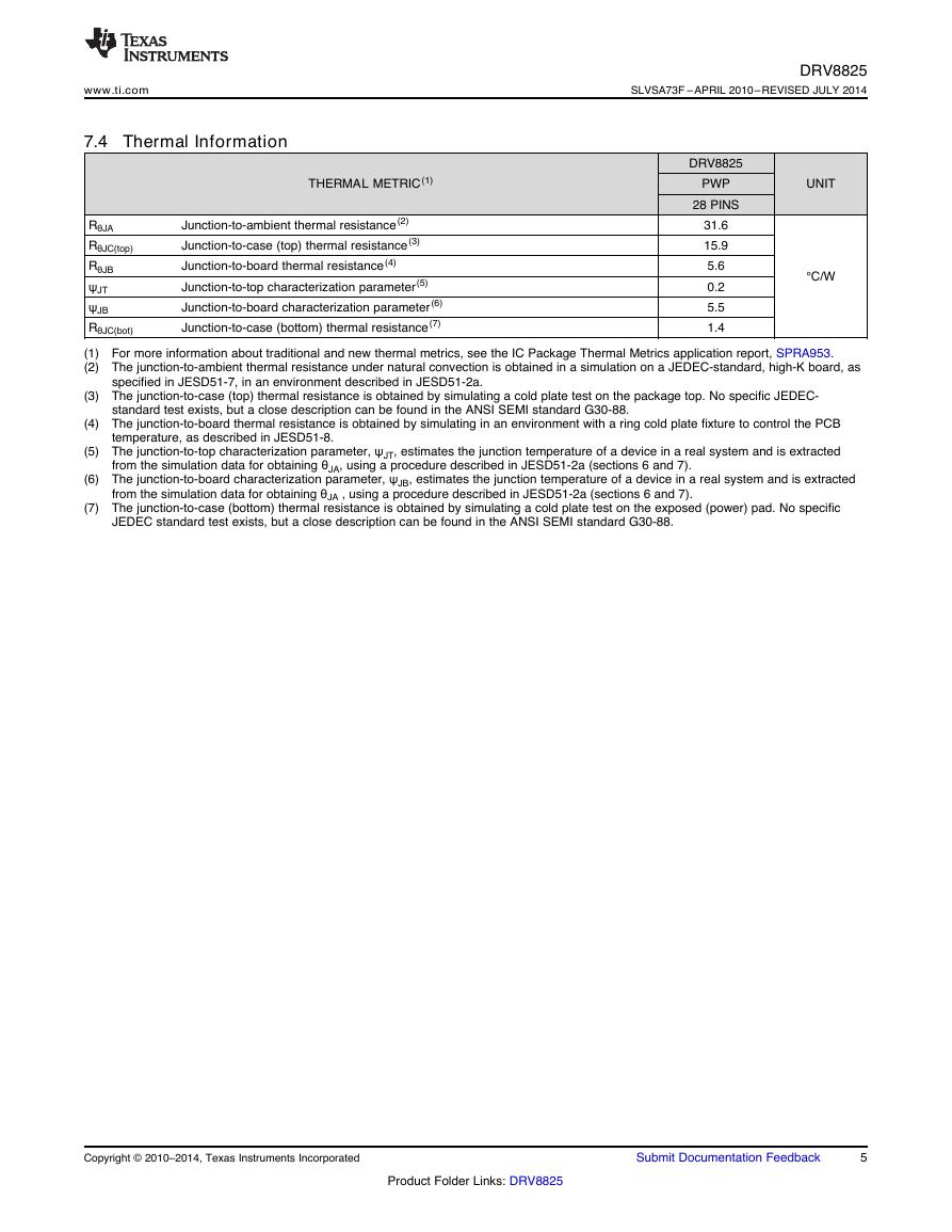
7.4 Thermal Information
THERMAL METRIC(1)
DRV8825
SLVSA73F –APRIL 2010–REVISED JULY 2014
DRV8825
PWP
28 PINS
UNIT
Junction-to-ambient thermal resistance(2)
Junction-to-case (top) thermal resistance(3)
Junction-to-board thermal resistance(4)
Junction-to-top characterization parameter(5)
Junction-to-board characterization parameter(6)
Junction-to-case (bottom) thermal resistance(7)
RθJA
RθJC(top)
RθJB
ψJT
ψJB
RθJC(bot)
(1) For more information about traditional and new thermal metrics, see the IC Package Thermal Metrics application report, SPRA953.
(2) The junction-to-ambient thermal resistance under natural convection is obtained in a simulation on a JEDEC-standard, high-K board, as
31.6
15.9
5.6
0.2
5.5
1.4
°C/W
specified in JESD51-7, in an environment described in JESD51-2a.
(3) The junction-to-case (top) thermal resistance is obtained by simulating a cold plate test on the package top. No specific JEDEC-
standard test exists, but a close description can be found in the ANSI SEMI standard G30-88.
(4) The junction-to-board thermal resistance is obtained by simulating in an environment with a ring cold plate fixture to control the PCB
temperature, as described in JESD51-8.
(5) The junction-to-top characterization parameter, ψJT, estimates the junction temperature of a device in a real system and is extracted
from the simulation data for obtaining θJA, using a procedure described in JESD51-2a (sections 6 and 7).
(6) The junction-to-board characterization parameter, ψJB, estimates the junction temperature of a device in a real system and is extracted
from the simulation data for obtaining θJA , using a procedure described in JESD51-2a (sections 6 and 7).
(7) The junction-to-case (bottom) thermal resistance is obtained by simulating a cold plate test on the exposed (power) pad. No specific
JEDEC standard test exists, but a close description can be found in the ANSI SEMI standard G30-88.
Spacer
Copyright © 2010–2014, Texas Instruments Incorporated
Submit Documentation Feedback
5
Product Folder Links: DRV8825
�
DRV8825
SLVSA73F –APRIL 2010–REVISED JULY 2014
www.ti.com
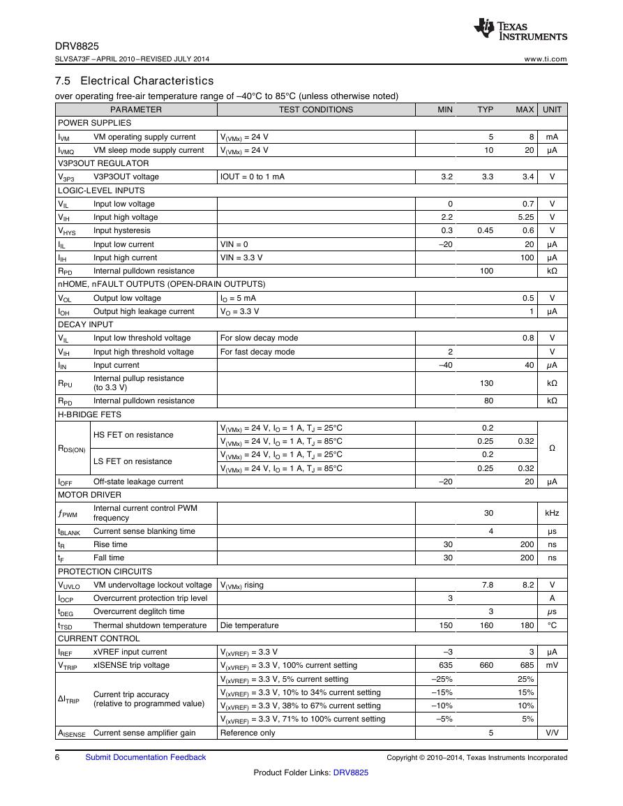
7.5 Electrical Characteristics
over operating free-air temperature range of –40°C to 85°C (unless otherwise noted)
PARAMETER
TEST CONDITIONS
MIN
TYP
MAX UNIT
V3P3OUT voltage
IOUT = 0 to 1 mA
VM operating supply current
VM sleep mode supply current
V(VMx) = 24 V
V(VMx) = 24 V
Input low voltage
Input high voltage
Input hysteresis
Input low current
Input high current
Internal pulldown resistance
POWER SUPPLIES
IVM
IVMQ
V3P3OUT REGULATOR
V3P3
LOGIC-LEVEL INPUTS
VIL
VIH
VHYS
IIL
IIH
RPD
nHOME, nFAULT OUTPUTS (OPEN-DRAIN OUTPUTS)
VOL
IOH
DECAY INPUT
VIL
VIH
IIN
RPU
RPD
H-BRIDGE FETS
Input low threshold voltage
Input high threshold voltage
Input current
Internal pullup resistance
(to 3.3 V)
Internal pulldown resistance
Output low voltage
Output high leakage current
VIN = 0
VIN = 3.3 V
IO = 5 mA
VO = 3.3 V
For slow decay mode
For fast decay mode
RDS(ON)
HS FET on resistance
LS FET on resistance
Off-state leakage current
IOFF
MOTOR DRIVER
V(VMx) = 24 V, IO = 1 A, TJ = 25°C
V(VMx) = 24 V, IO = 1 A, TJ = 85°C
V(VMx) = 24 V, IO = 1 A, TJ = 25°C
V(VMx) = 24 V, IO = 1 A, TJ = 85°C
Internal current control PWM
frequency
Current sense blanking time
Rise time
Fall time
ƒPWM
tBLANK
tR
tF
PROTECTION CIRCUITS
VUVLO
IOCP
tDEG
tTSD
CURRENT CONTROL
IREF
VTRIP
xVREF input current
xISENSE trip voltage
VM undervoltage lockout voltage V(VMx) rising
Overcurrent protection trip level
Overcurrent deglitch time
Thermal shutdown temperature
Die temperature
ΔITRIP
Current trip accuracy
(relative to programmed value)
AISENSE Current sense amplifier gain
6
Submit Documentation Feedback
5
10
3.3
0.45
100
130
80
0.2
0.25
0.2
0.25
30
4
7.8
3
160
660
5
8 mA
μA
20
3.4
V
0.7
5.25
0.6
20
100
0.5
1
0.8
40
0.32
0.32
20
200
200
8.2
180
V
V
V
μA
μA
kΩ
V
μA
V
V
µA
kΩ
kΩ
Ω
μA
kHz
μs
ns
ns
V
A
µs
°C
3
μA
685 mV
25%
15%
10%
5%
V/V
3.2
0
2.2
0.3
–20
2
–40
–20
30
30
3
150
–3
635
–25%
–15%
–10%
–5%
V(xVREF) = 3.3 V
V(xVREF) = 3.3 V, 100% current setting
V(xVREF) = 3.3 V, 5% current setting
V(xVREF) = 3.3 V, 10% to 34% current setting
V(xVREF) = 3.3 V, 38% to 67% current setting
V(xVREF) = 3.3 V, 71% to 100% current setting
Reference only
Product Folder Links: DRV8825
Copyright © 2010–2014, Texas Instruments Incorporated
�
www.ti.com
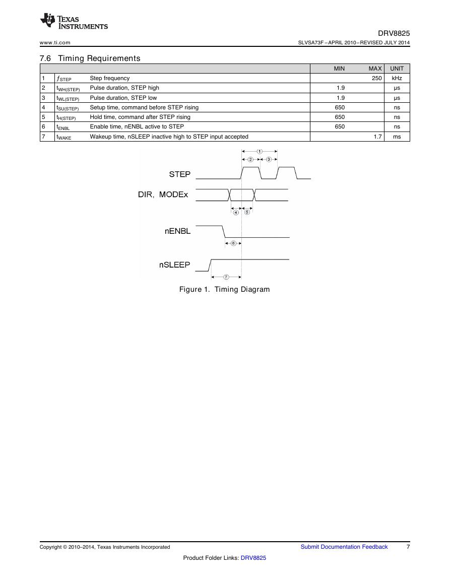
7.6 Timing Requirements
1
2
3
4
5
6
7
ƒSTEP
tWH(STEP)
tWL(STEP)
tSU(STEP)
tH(STEP)
tENBL
tWAKE
Step frequency
Pulse duration, STEP high
Pulse duration, STEP low
Setup time, command before STEP rising
Hold time, command after STEP rising
Enable time, nENBL active to STEP
Wakeup time, nSLEEP inactive high to STEP input accepted
DRV8825
SLVSA73F –APRIL 2010–REVISED JULY 2014
MIN
1.9
1.9
650
650
650
MAX UNIT
kHz
250
μs
μs
ns
ns
ns
ms
1.7
Figure 1. Timing Diagram
Copyright © 2010–2014, Texas Instruments Incorporated
Submit Documentation Feedback
7
Product Folder Links: DRV8825
�
DRV8825
SLVSA73F –APRIL 2010–REVISED JULY 2014
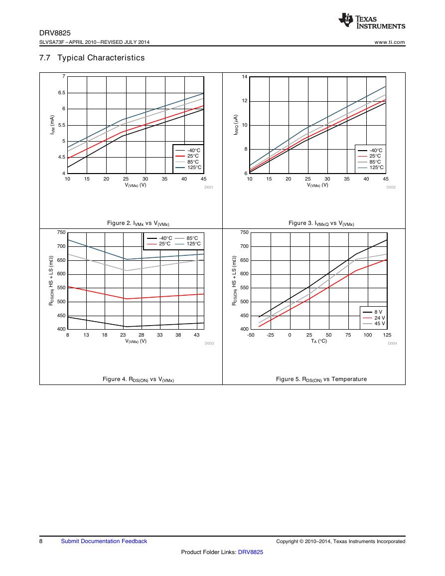
7.7 Typical Characteristics
www.ti.com
Figure 2. IVMx vs V(VMx)
Figure 3. IVMxQ vs V(VMx)
Figure 4. RDS(ON) vs V(VMx)
Figure 5. RDS(ON) vs Temperature
8
Submit Documentation Feedback
Copyright © 2010–2014, Texas Instruments Incorporated
Product Folder Links: DRV8825
V(VMx) (V)RDS(ON) HS + LS (m�)813182328333843400450500550600650700750D003-40GC25GC85GC125GCTA (GC)RDS(ON) HS + LS (m�)-50-250255075100125400450500550600650700750D0048 V24 V45 VV(VMx) (V)IVM (mA)101520253035404544.555.566.57D001-40GC25GC85GC125GCV(VMx) (V)IVMQ (2A)101520253035404568101214D002-40GC25GC85GC125GC�


 V2版本原理图(Capacitive-Fingerprint-Reader-Schematic_V2).pdf
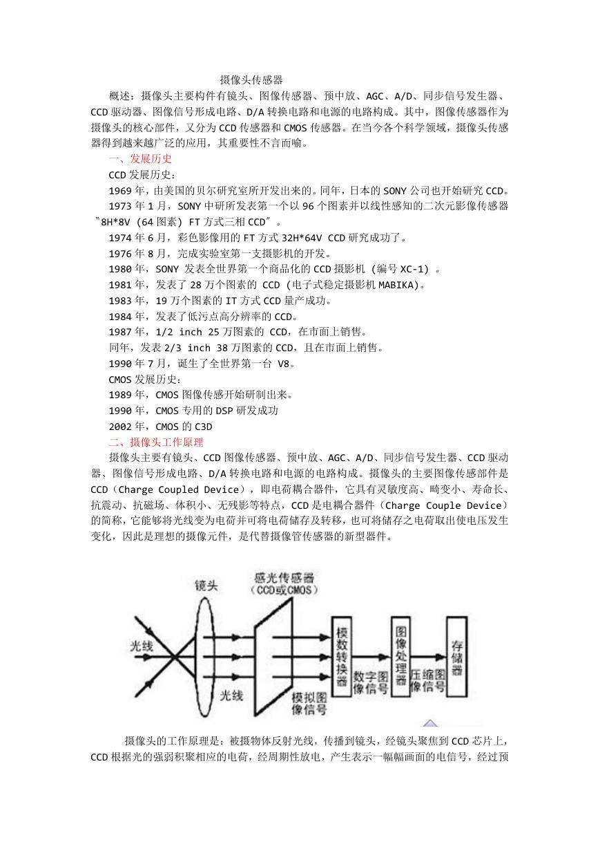 摄像头工作原理.doc
 VL53L0X简要说明(En.FLVL53L00216).pdf
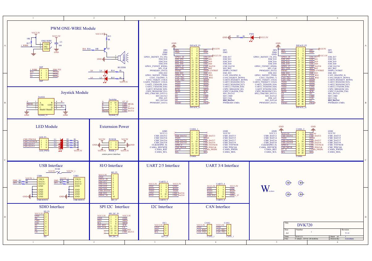 原理图(DVK720-Schematic).pdf
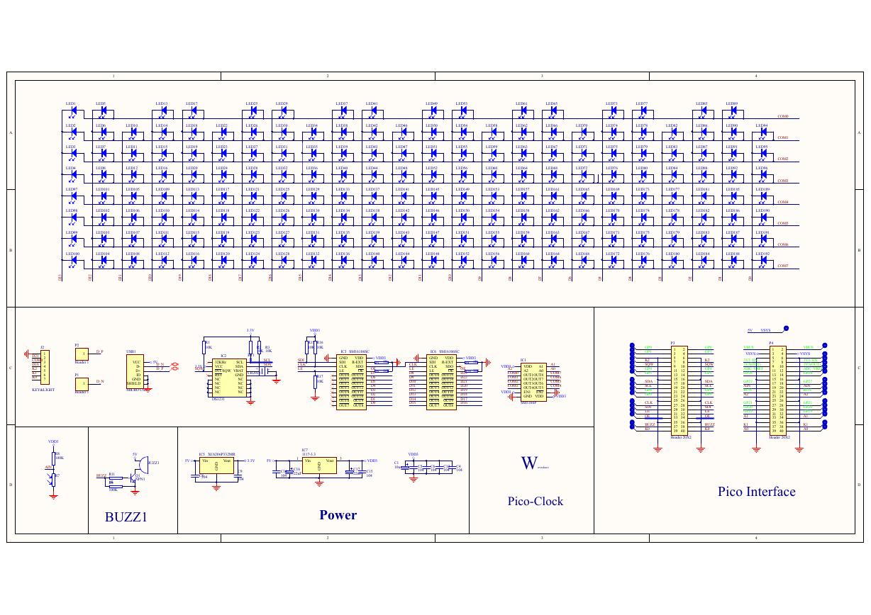 原理图(Pico-Clock-Green-Schdoc).pdf
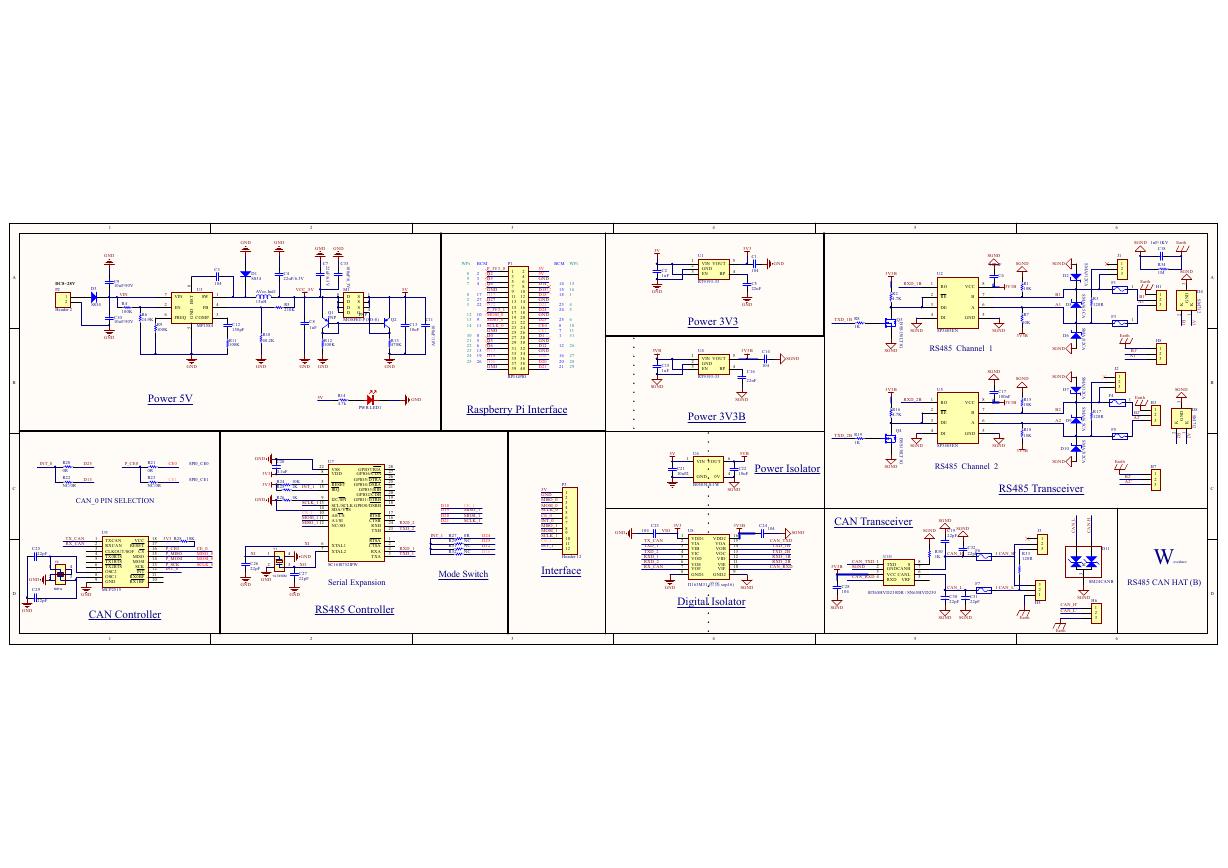 原理图(RS485-CAN-HAT-B-schematic).pdf
 File:SIM7500_SIM7600_SIM7800 Series_SSL_Application Note_V2.00.pdf
 ADS1263(Ads1262).pdf
 原理图(Open429Z-D-Schematic).pdf
 用户手册(Capacitive_Fingerprint_Reader_User_Manual_CN).pdf
 CY7C68013A(英文版)(CY7C68013A).pdf
 TechnicalReference_Dem.pdf