SN65HVD230
SN65HVD231
SN65HVD232
SLOS346G – MARCH 2001 – REVISED JUNE 2002
3.3-V CAN TRANSCEIVERS
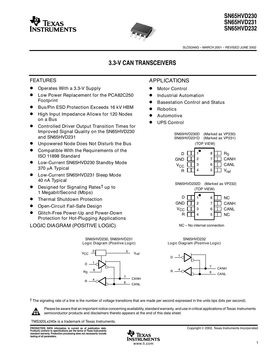
FEATURES
D Operates With a 3.3-V Supply
D Low Power Replacement for the PCA82C250
Footprint
D Bus/Pin ESD Protection Exceeds 16 kV HBM
D High Input Impedance Allows for 120 Nodes
on a Bus
D Controlled Driver Output Transition Times for
Improved Signal Quality on the SN65HVD230
and SN65HVD231
D Unpowered Node Does Not Disturb the Bus
D Compatible With the Requirements of the
ISO 11898 Standard
D Low-Current SN65HVD230 Standby Mode
370 µA Typical
D Low-Current SN65HVD231 Sleep Mode
40 nA Typical
D Designed for Signaling Rates† up to
1 Megabit/Second (Mbps)
D Thermal Shutdown Protection
D Open-Circuit Fail-Safe Design
D Glitch-Free Power-Up and Power-Down
Protection for Hot-Plugging Applications
LOGIC DIAGRAM (POSITIVE LOGIC)
APPLICATIONS
D Motor Control
D Industrial Automation
D Basestation Control and Status
D Robotics
D Automotive
D UPS Control
SN65HVD230D (Marked as VP230)
SN65HVD231D (Marked as VP231)
(TOP VIEW)
1
2
3
4
8
7
6
5
RS
CANH
CANL
Vref
D
GND
VCC
R
SN65HVD232D (Marked as VP232)
(TOP VIEW)
D
GND
VCC
R
1
2
3
4
8
7
6
5
NC
CANH
CANL
NC
NC – No internal connection
SN65HVD230, SN65HVD231
Logic Diagram (Positive Logic)
SN65HVD232
Logic Diagram (Positive Logic)
3
1
8
4
VCC
D
RS
R
5
Vref
7
6
CANH
CANL
1
4
D
R
7
6
CANH
CANL
† The signaling rate of a line is the number of voltage transitions that are made per second expressed in the units bps (bits per second).
Please be aware that an important notice concerning availability, standard warranty, and use in critical applications of Texas Instruments
semiconductor products and disclaimers thereto appears at the end of this data sheet.
TMS320Lx240x is a trademark of Texas Instruments.
PRODUCTION DATA information is current as of publication date.
Products conform to specifications per the terms of Texas Instruments
standard warranty. Production processing does not necessarily include
testing of all parameters.
Copyright 2002, Texas Instruments Incorporated
www.ti.com
1
�
SN65HVD230
SN65HVD231
SN65HVD232
SLOS346G – MARCH 2001 – REVISED JUNE 2002
DESCRIPTION
The SN65HVD230, SN65HVD231, and SN65HVD232 controller area network (CAN) transceivers are designed
for use with the Texas Instruments TMS320Lx240x 3.3-V DSPs with CAN controllers, or with equivalent
devices. They are intended for use in applications employing the CAN serial communication physical layer in
accordance with the ISO 11898 standard. Each CAN transceiver is designed to provide differential transmit
capability to the bus and differential receive capability to a CAN controller at speeds up to 1 Mbps.
Designed for operation in especially-harsh environments, these devices feature cross-wire protection,
loss-of-ground and overvoltage protection, overtemperature protection, as well as wide common-mode range.
The transceiver interfaces the single-ended CAN controller with the differential CAN bus found in industrial,
building automation, and automotive applications. It operates over a –2-V to 7-V common-mode range on the
bus, and it can withstand common-mode transients of ±25 V.
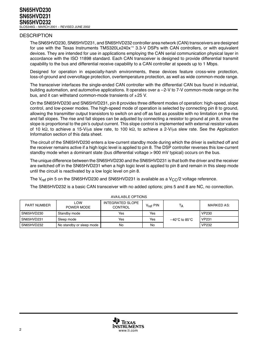
On the SN65HVD230 and SN65HVD231, pin 8 provides three different modes of operation: high-speed, slope
control, and low-power modes. The high-speed mode of operation is selected by connecting pin 8 to ground,
allowing the transmitter output transistors to switch on and off as fast as possible with no limitation on the rise
and fall slopes. The rise and fall slopes can be adjusted by connecting a resistor to ground at pin 8, since the
slope is proportional to the pin’s output current. This slope control is implemented with external resistor values
of 10 kΩ, to achieve a 15-V/µs slew rate, to 100 kΩ, to achieve a 2-V/µs slew rate. See the Application
Information section of this data sheet.
The circuit of the SN65HVD230 enters a low-current standby mode during which the driver is switched off and
the receiver remains active if a high logic level is applied to pin 8. The DSP controller reverses this low-current
standby mode when a dominant state (bus differential voltage > 900 mV typical) occurs on the bus.
The unique difference between the SN65HVD230 and the SN65HVD231 is that both the driver and the receiver
are switched off in the SN65HVD231 when a high logic level is applied to pin 8 and remain in this sleep mode
until the circuit is reactivated by a low logic level on pin 8.
The Vref pin 5 on the SN65HVD230 and SN65HVD231 is available as a VCC/2 voltage reference.
The SN65HVD232 is a basic CAN transceiver with no added options; pins 5 and 8 are NC, no connection.
AVAILABLE OPTIONS
PART NUMBER
LOW
POWER MODE
INTEGRATED SLOPE
CONTROL
Vref PIN
TA
MARKED AS:
SN65HVD230
SN65HVD231
SN65HVD232
Standby mode
Sleep mode
No standby or sleep mode
Yes
Yes
No
Yes
Yes
No
– 40°C to 85°C
40 C to 85 C
VP230
VP231
VP232
2
www.ti.com
�
SN65HVD230
SN65HVD231
SN65HVD232
SLOS346G – MARCH 2001 – REVISED JUNE 2002
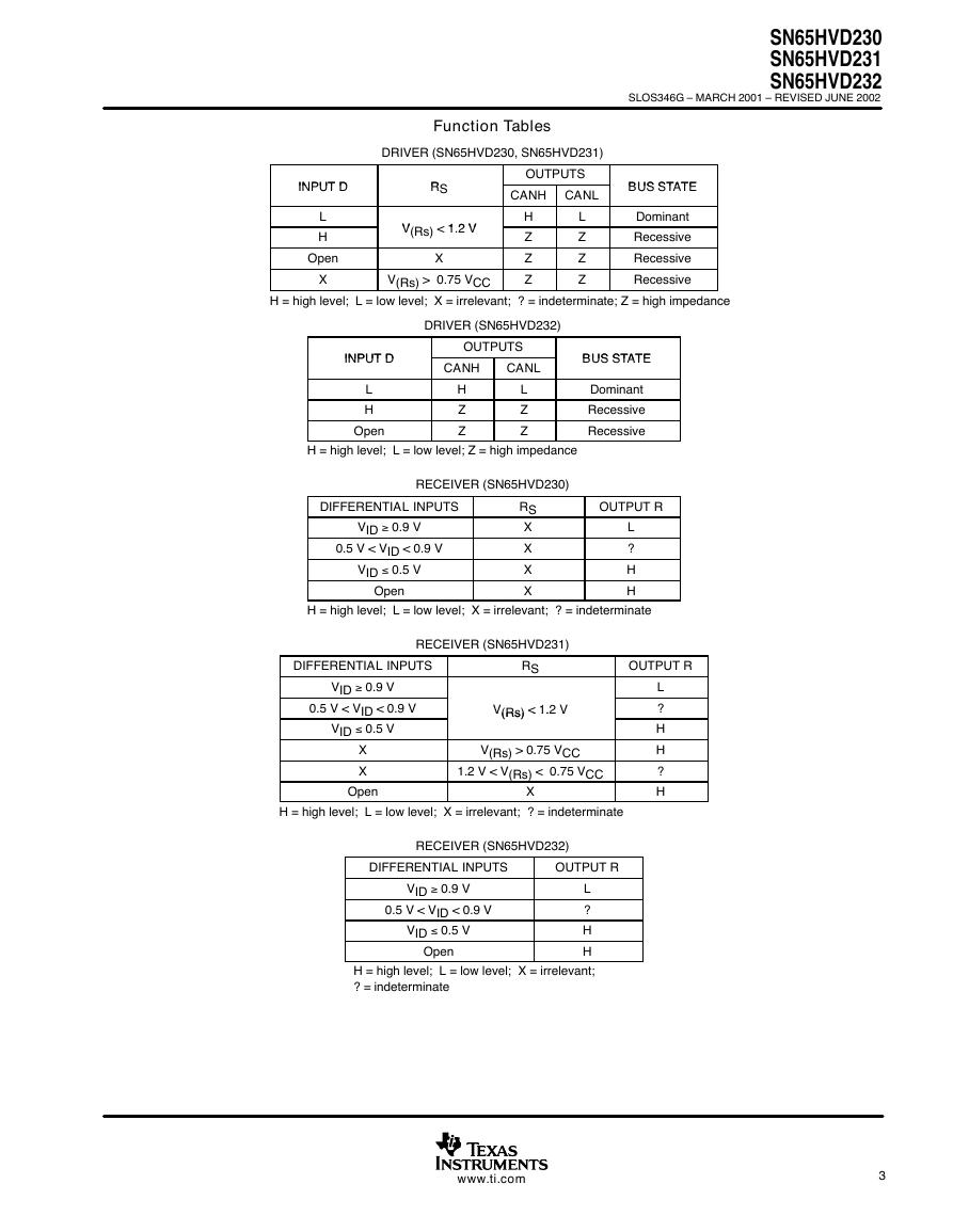
Function Tables
DRIVER (SN65HVD230, SN65HVD231)
INPUT D
INPUT D
R
RS
L
H
Open
X
V
1 2 V
V(Rs) < 1.2 V
X
V(Rs) > 0.75 VCC
OUTPUTS
CANH
CANL
H
Z
Z
Z
L
Z
Z
Z
BUS STATE
BUS STATE
Dominant
Recessive
Recessive
Recessive
H = high level; L = low level; X = irrelevant; ? = indeterminate; Z = high impedance
DRIVER (SN65HVD232)
OUTPUTS
CANH
CANL
H
Z
Z
L
Z
Z
BUS STATE
BUS STATE
Dominant
Recessive
Recessive
INPUT D
INPUT D
L
H
Open
H = high level; L = low level; Z = high impedance
RECEIVER (SN65HVD230)
DIFFERENTIAL INPUTS
VID ≥ 0.9 V
0.5 V < VID < 0.9 V
VID ≤ 0.5 V
Open
RS
X
X
X
X
OUTPUT R
L
?
H
H
H = high level; L = low level; X = irrelevant; ? = indeterminate
RECEIVER (SN65HVD231)
RS
OUTPUT R
V(Rs) < 1.2 V
V(Rs) < 1.2 V
L
?
H
H
?
H
DIFFERENTIAL INPUTS
VID ≥ 0.9 V
0.5 V < VID < 0.9 V
VID ≤ 0.5 V
X
X
Open
V(Rs) > 0.75 VCC
1.2 V < V(Rs) < 0.75 VCC
X
H = high level; L = low level; X = irrelevant; ? = indeterminate
RECEIVER (SN65HVD232)
DIFFERENTIAL INPUTS
OUTPUT R
VID ≥ 0.9 V
0.5 V < VID < 0.9 V
L
?
H
H
H = high level; L = low level; X = irrelevant;
? = indeterminate
VID ≤ 0.5 V
Open
www.ti.com
3
�
SN65HVD230
SN65HVD231
SN65HVD232
SLOS346G – MARCH 2001 – REVISED JUNE 2002
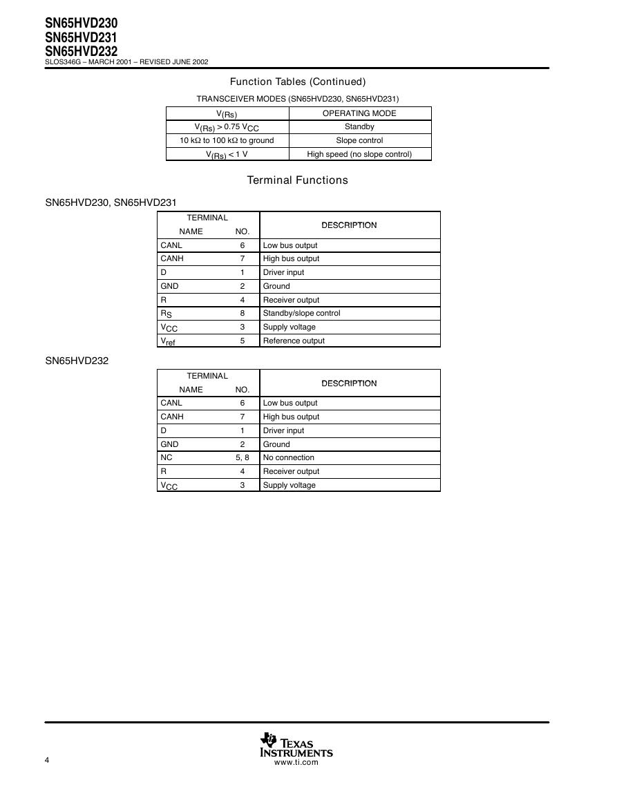
Function Tables (Continued)
TRANSCEIVER MODES (SN65HVD230, SN65HVD231)
OPERATING MODE
V(Rs)
V(Rs) > 0.75 VCC
10 kΩ to 100 kΩ to ground
Standby
Slope control
V(Rs) < 1 V
High speed (no slope control)
Terminal Functions
SN65HVD230, SN65HVD231
TERMINAL
NAME
NO.
DESCRIPTION
DESCRIPTION
SN65HVD232
CANL
CANH
D
GND
R
RS
VCC
Vref
TERMINAL
NAME
CANL
CANH
D
GND
NC
R
VCC
6
7
1
2
4
8
3
5
NO.
6
7
1
2
5, 8
4
3
Low bus output
High bus output
Driver input
Ground
Receiver output
Standby/slope control
Supply voltage
Reference output
DESCRIPTION
DESCRIPTION
Low bus output
High bus output
Driver input
Ground
No connection
Receiver output
Supply voltage
4
www.ti.com
�
SN65HVD230
SN65HVD231
SN65HVD232
SLOS346G – MARCH 2001 – REVISED JUNE 2002
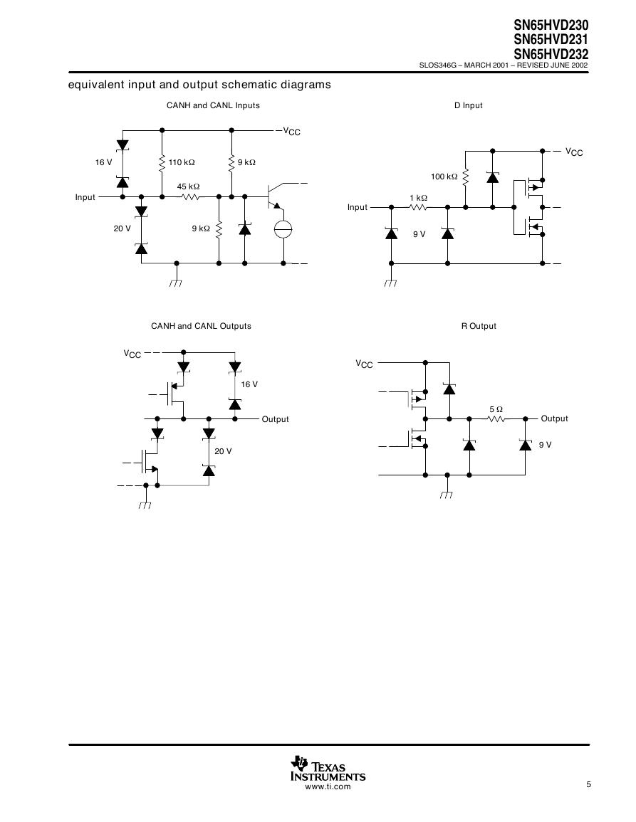
equivalent input and output schematic diagrams
CANH and CANL Inputs
D Input
16 V
Input
9 kΩ
110 kΩ
45 kΩ
20 V
9 kΩ
VCC
VCC
Input
100 kΩ
1 kΩ
9 V
CANH and CANL Outputs
R Output
VCC
VCC
16 V
Output
20 V
5 Ω
Output
9 V
www.ti.com
5
�
SN65HVD230
SN65HVD231
SN65HVD232
SLOS346G – MARCH 2001 – REVISED JUNE 2002
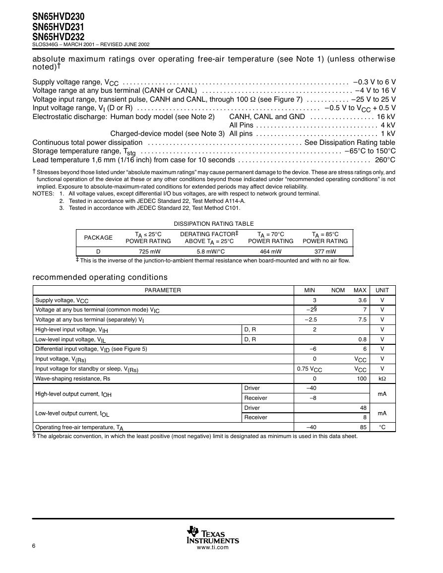
absolute maximum ratings over operating free-air temperature (see Note 1) (unless otherwise
noted)†
. . . . . . . . . . . . . . . . . . . . . . . . . . . . . . . . . . . . . . . . . . . . . . . . . . .
. . . . . . . . . . . . . . . . . . . . . . . . . . . . . . . . . . . . . . . . . . . . . . . . . . . . . . . . . . . . . . .
. . . . . . . . . . . . . . . . . . . . . . . . . . . . . . . . . . . . . . . . . .
. . . . . . . . . . . .
Supply voltage range, VCC
Voltage range at any bus terminal (CANH or CANL)
Voltage input range, transient pulse, CANH and CANL, through 100 Ω (see Figure 7)
Input voltage range, VI (D or R)
Electrostatic discharge: Human body model (see Note 2)
–0.3 V to 6 V
–4 V to 16 V
–25 V to 25 V
–0.5 V to VCC + 0.5 V
16 kV
4 kV
1 kV
See Dissipation Rating table
Continuous total power dissipation
–65°C to 150°C
Storage temperature range, Tstg
260°C
Lead temperature 1,6 mm (1/16 inch) from case for 10 seconds
† Stresses beyond those listed under “absolute maximum ratings” may cause permanent damage to the device. These are stress ratings only, and
functional operation of the device at these or any other conditions beyond those indicated under “recommended operating conditions” is not
implied. Exposure to absolute-maximum-rated conditions for extended periods may affect device reliability.
CANH, CANL and GND
All Pins
Charged-device model (see Note 3) All pins
. . . . . . . . . . . . . . . . . .
. . . . . . . . . . . . . . . . . . . . . . . . . . . . . . . . . .
. . . . . . . . . . . . . . . . . . . . . . . . . . . . . . . . . .
. . . . . . . . . . . . . . . . . . . . . . . . . . . . . . . . . . . . . . . . . . .
. . . . . . . . . . . . . . . . . . . . . . . . . . . . . . . . . . . . . . . . . . . . . . . . . . . . . . . .
. . . . . . . . . . . . . . . . . . . . . . . . . . . . . . . . . . . . .
NOTES: 1. All voltage values, except differential I/O bus voltages, are with respect to network ground terminal.
2. Tested in accordance with JEDEC Standard 22, Test Method A114-A.
3. Tested in accordance with JEDEC Standard 22, Test Method C101.
DISSIPATION RATING TABLE
PACKAGE
TA ≤ 25°C
POWER RATING
DERATING FACTOR‡
ABOVE TA = 25°C
TA = 70°C
POWER RATING
TA = 85°C
POWER RATING
D
725 mW
5.8 mW/°C
464 mW
377 mW
‡ This is the inverse of the junction-to-ambient thermal resistance when board-mounted and with no air flow.
NOM MAX
3.6
7
7.5
0.8
6
VCC
VCC
100
MIN
3
– 2§
– 2.5
2
–6
0
0.75 VCC
0
–40
–8
48
8
85
recommended operating conditions
PARAMETER
Supply voltage, VCC
Voltage at any bus terminal (common mode) VIC
Voltage at any bus terminal (separately) VI
High-level input voltage, VIH
Low-level input voltage, VIL
Differential input voltage, VID (see Figure 5)
Input voltage, V(Rs)
Input voltage for standby or sleep, V(Rs)
Wave-shaping resistance, Rs
High level output current I
High-level output current, IOH
Low level output current I
Low-level output current, IOL
D, R
D, R
Driver
Receiver
Driver
Receiver
Operating free-air temperature, TA
§ The algebraic convention, in which the least positive (most negative) limit is designated as minimum is used in this data sheet.
–40
6
www.ti.com
UNIT
V
V
V
V
V
V
V
V
kΩ
mA
mA
mA
mA
°C
�
SN65HVD230
SN65HVD231
SN65HVD232
SLOS346G – MARCH 2001 – REVISED JUNE 2002
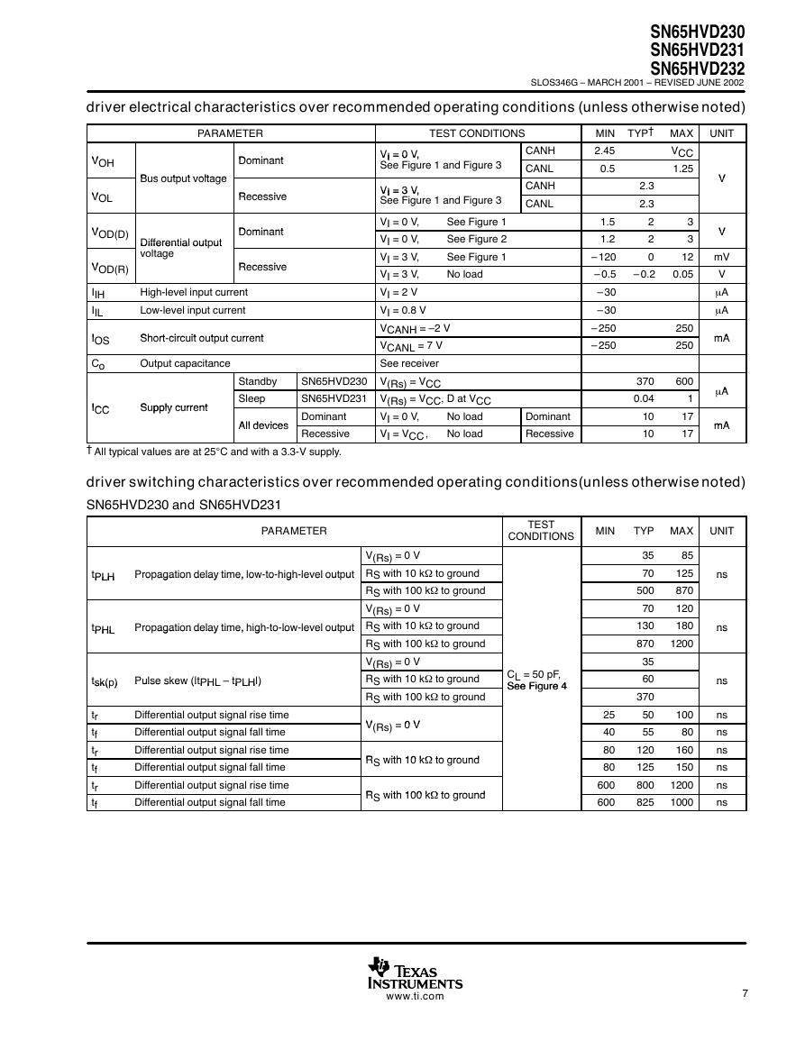
driver electrical characteristics over recommended operating conditions (unless otherwise noted)
PARAMETER
TEST CONDITIONS
V
VOH
V
VOL
V
VOD(D)
V
VOD(R)
IIH
IIL
I
IOS
Co
ICC
ICC
Bus output voltage
Bus output voltage
Differential output
Differential out ut
voltage
Dominant
Dominant
Recessive
Recessive
Dominant
Dominant
Recessive
Recessive
High-level input current
Low-level input current
Short circuit output current
Short-circuit output current
Output capacitance
Supply current
Supply current
Standby
Sleep
All devices
All devices
MIN TYP† MAX
VCC
2.45
0.5
1.25
1.5
1.2
– 120
– 0.5
– 30
– 30
– 250
– 250
2.3
2.3
2
2
0
– 0.2
370
0.04
10
10
3
3
12
0.05
250
250
600
1
17
17
UNIT
V
V
V
V
mV
V
µA
µA
mA
mA
µA
A
mA
mA
VI = 0 V,
VI = 0 V,
See Figure 1 and Figure 3
VI = 3 V,
VI = 3 V,
See Figure 1 and Figure 3
CANH
CANL
CANH
CANL
See Figure 1
See Figure 2
See Figure 1
No load
VI = 0 V,
VI = 0 V,
VI = 3 V,
VI = 3 V,
VI = 2 V
VI = 0.8 V
VCANH = –2 V
VCANL = 7 V
See receiver
SN65HVD230 V(Rs) = VCC
SN65HVD231 V(Rs) = VCC, D at VCC
Dominant
Recessive
No load
No load
VI = 0 V,
VI = VCC ,
Dominant
Recessive
† All typical values are at 25°C and with a 3.3-V supply.
driver switching characteristics over recommended operating conditions(unless otherwise noted)
SN65HVD230 and SN65HVD231
PARAMETER
TEST
CONDITIONS
MIN
TYP MAX
UNIT
V(Rs) = 0 V
Propagation delay time, low-to-high-level output RS with 10 kΩ to ground
Pro agation delay time, low to high level out ut
RS with 100 kΩ to ground
V(Rs) = 0 V
Propagation delay time, high-to-low-level output RS with 10 kΩ to ground
Pro agation delay time, high to low level out ut
RS with 100 kΩ to ground
V(Rs) = 0 V
RS with 10 kΩ to ground
RS with 100 kΩ to ground
Pulse skew (|tPHL – tPLH|)
Pulse skew (|tPHL tPLH|)
Differential output signal rise time
Differential output signal fall time
Differential output signal rise time
Differential output signal fall time
Differential output signal rise time
Differential output signal fall time
V
0 V
V(Rs) = 0 V
R with 10 kΩ to ground
RS with 10 kΩ to ground
R with 100 kΩ to ground
RS with 100 kΩ to ground
CL = 50 pF,
See Figure 4
See Figure 4
35
70
500
70
130
870
35
60
370
50
55
120
125
800
825
85
125
870
120
180
1200
100
80
160
150
1200
1000
ns
ns
ns
ns
ns
ns
ns
ns
ns
ns
ns
ns
25
40
80
80
600
600
tPLH
tPLH
tPHL
tPHL
tsk(p)
tsk( )
tr
tf
tr
tf
tr
tf
www.ti.com
7
�
SN65HVD230
SN65HVD231
SN65HVD232
SLOS346G – MARCH 2001 – REVISED JUNE 2002
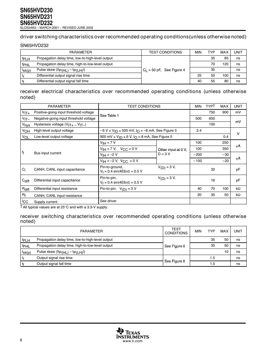
driver switching characteristics over recommended operating conditions(unless otherwise noted)
SN65HVD232
PARAMETER
TEST CONDITIONS
MIN
tPLH
tPHL
tsk(p)
tr
tf
Propagation delay time, low-to-high-level output
Propagation delay time, high-to-low-level output
Pulse skew (|tP(HL) – tP(LH)|)
Differential output signal rise time
Differential output signal fall time
CL = 50 pF, See Figure 4
CL
50 F, See Figure 4
25
40
TYP MAX
85
120
100
80
receiver electrical characteristics over recommended operating conditions (unless otherwise
noted)
PARAMETER
TEST CONDITIONS
See Table 1
See Table 1
MIN TYP† MAX
900
VIT+ Positive-going input threshold voltage
VIT– Negative-going input threshold voltage
Vhys Hysteresis voltage (VIT+ – VIT–)
VOH High-level output voltage
VOL
Low-level output voltage
I
II
Ci
Bus input current
CANH, CANL input capacitance
Cdiff Differential input capacitance
Rdiff Differential input resistance
RI
ICC
† All typical values are at 25°C and with a 3.3-V supply.
CANH, CANL input resistance
Supply current
See driver
35
70
35
50
55
750
650
100
500
2.4
100
100
– 200
– 100
40
20
0.4
250
350
– 30
– 20
100
50
32
16
70
35
UNIT
ns
ns
ns
ns
ns
UNIT
mV
mV
mV
V
V
µA
A
µA
A
pF
pF
kΩ
kΩ
– 6 V ≤ VID ≤ 500 mV, IO = –8 mA, See Figure 5
900 mV ≤ VID ≤ 6 V, IO = 8 mA, See Figure 5
VIH = 7 V
VIH = 7 V, VCC = 0 V
VIH = –2 V
VIH = –2 V, VCC = 0 V
Pin-to-ground,
VI = 0.4 sin(4E6πt) + 0.5 V
Pin-to-pin,
VI = 0.4 sin(4E6πt) + 0.5 V
Pin-to-pin, V(D) = 3 V
V(D) = 3 V,
V(D) = 3 V,
Other input at 0 V,
Other in ut at 0 V,
D = 3 V
receiver switching characteristics over recommended operating conditions (unless otherwise
noted)
PARAMETER
tPLH
tPHL
tsk(p)
tr
tf
Propagation delay time, low-to-high-level output
Propagation delay time, high-to-low-level output
Pulse skew (|tP(HL) – tP(LH)|)
Output signal rise time
Output signal fall time
TEST
CONDITIONS
See Figure 6
See Figure 6
See Figure 6
See Figure 6
MIN
TYP MAX
UNIT
35
35
1.5
1.5
50
50
10
ns
ns
ns
ns
ns
8
www.ti.com
�


 V2版本原理图(Capacitive-Fingerprint-Reader-Schematic_V2).pdf
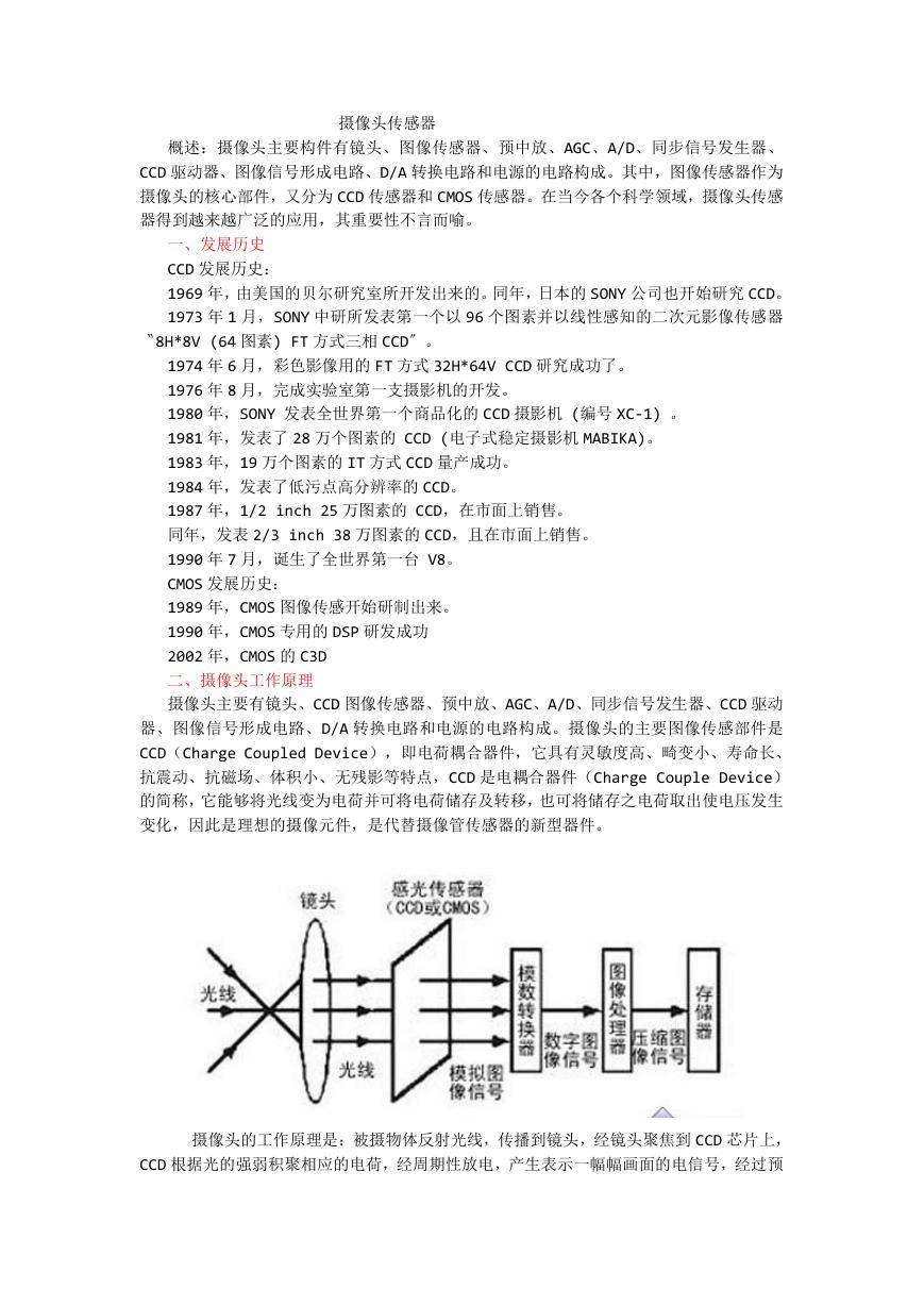 摄像头工作原理.doc
 VL53L0X简要说明(En.FLVL53L00216).pdf
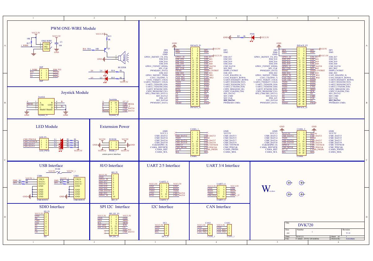 原理图(DVK720-Schematic).pdf
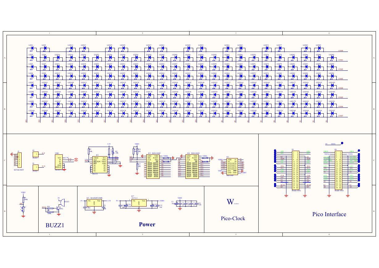 原理图(Pico-Clock-Green-Schdoc).pdf
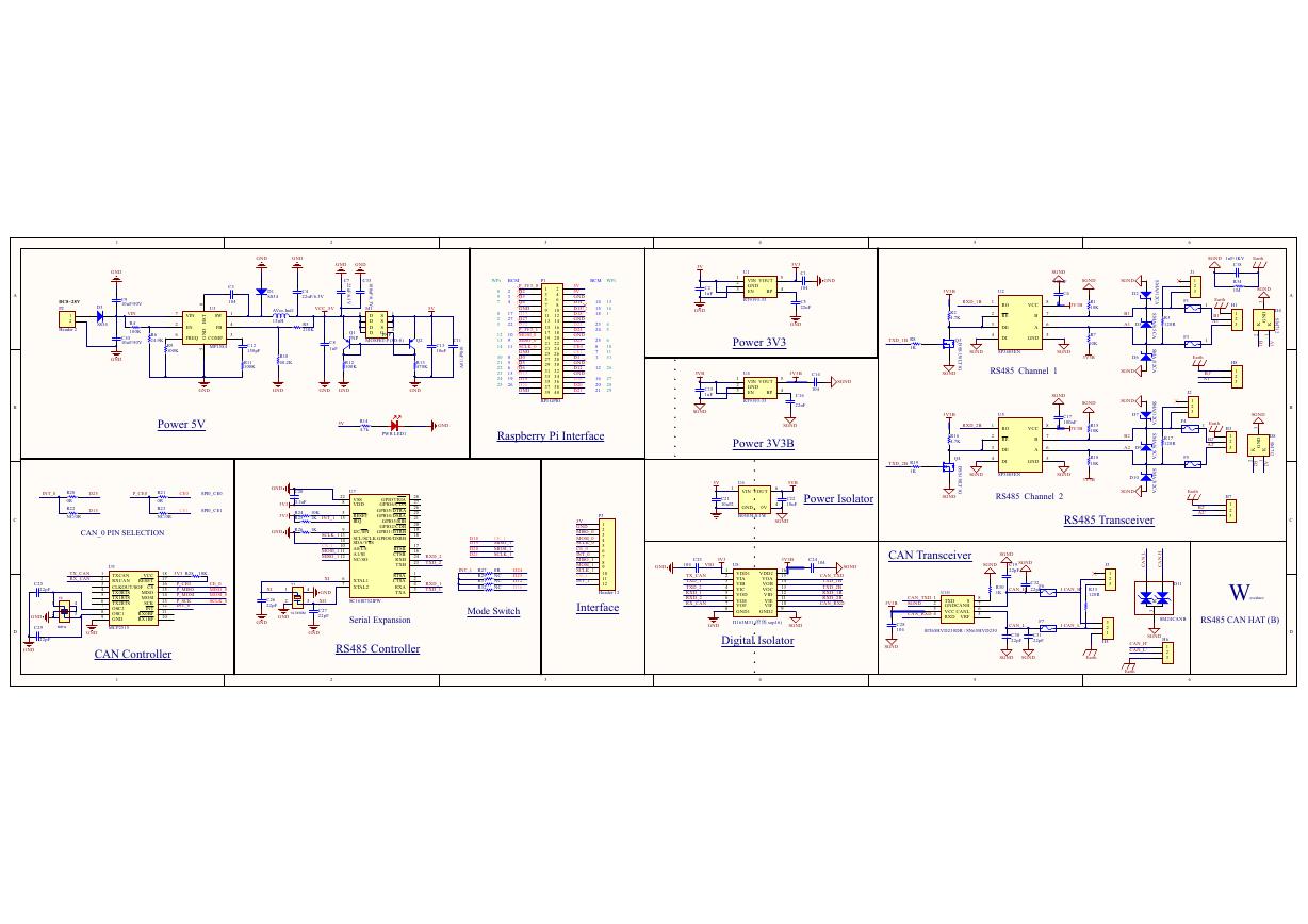 原理图(RS485-CAN-HAT-B-schematic).pdf
 File:SIM7500_SIM7600_SIM7800 Series_SSL_Application Note_V2.00.pdf
 ADS1263(Ads1262).pdf
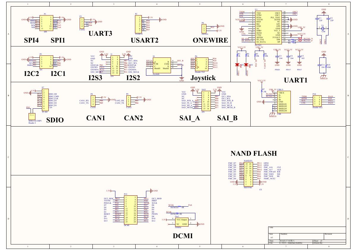 原理图(Open429Z-D-Schematic).pdf
 用户手册(Capacitive_Fingerprint_Reader_User_Manual_CN).pdf
 CY7C68013A(英文版)(CY7C68013A).pdf
 TechnicalReference_Dem.pdf