PRELIMINARY PRODUCT SPECIFICATION
Single chip 2.4 GHz Transceiver
nRF24L01
FEATURES
• True single chip GFSK transceiver
• Complete OSI Link Layer in hardware
• Enhanced ShockBurst™
• Auto ACK & retransmit
• Address and CRC computation
• On the air data rate 1 or 2Mbps
• Digital interface (SPI) speed 0-10 Mbps
• 125 RF channel operation
• Short switching time enable frequency hopping
• Fully RF compatible with nRF24XX
• 5V tolerant signal input pads
• 20-pin package (QFN20 4x4mm)
• Uses ultra low cost +/- 60 ppm crystal
• Uses low cost chip inductors and 2-layer PCB
• Power supply range: 1.9 to 3.6 V
APPLICATIONS
• Wireless mouse, keyboard, joystick
• Keyless entry
• Wireless data communication
• Alarm and security systems
• Home automation
• Surveillance
• Automotive
• Telemetry
•
•
• Toys
Intelligent sports equipment
Industrial sensors
GENERAL DESCRIPTION
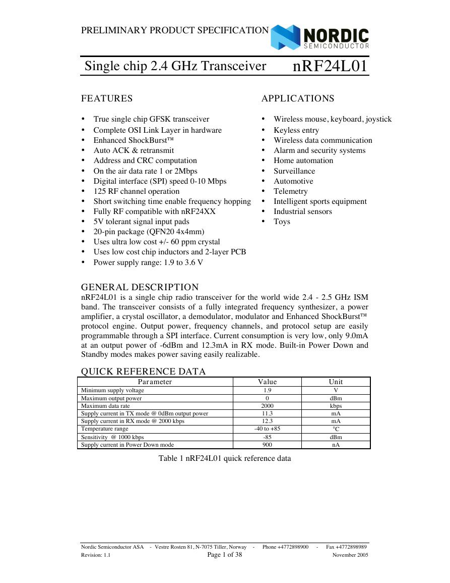
nRF24L01 is a single chip radio transceiver for the world wide 2.4 - 2.5 GHz ISM
band. The transceiver consists of a fully integrated frequency synthesizer, a power
amplifier, a crystal oscillator, a demodulator, modulator and Enhanced ShockBurst™
protocol engine. Output power, frequency channels, and protocol setup are easily
programmable through a SPI interface. Current consumption is very low, only 9.0mA
at an output power of -6dBm and 12.3mA in RX mode. Built-in Power Down and
Standby modes makes power saving easily realizable.
QUICK REFERENCE DATA
Parameter
Minimum supply voltage
Maximum output power
Maximum data rate
Supply current in TX mode @ 0dBm output power
Supply current in RX mode @ 2000 kbps
Temperature range
Sensitivity @ 1000 kbps
Supply current in Power Down mode
Value
1.9
0
2000
11.3
12.3
-40 to +85
-85
900
Table 1 nRF24L01 quick reference data
Unit
V
dBm
kbps
mA
mA
C
dBm
nA
Nordic Semiconductor ASA
Revision: 1.1
- Vestre Rosten 81, N-7075 Tiller, Norway
-
Phone +4772898900
-
Page 1 of 38
Fax +4772898989
November 2005
�
PRELIMINARY PRODUCT SPECIFICATION
nRF24L01 Single Chip 2.4 GHz Radio Transceiver
Type Number
nRF24L01
nRF24L01 IC
Description
20 pin QFN 4x4, lead free (green)
Bare Dice
nRF24L01-EVKIT
Evaluation kit (2 test PCB, 2 configuration PCB, SW)
Version
A
A
1.0
Table 2 nRF24L01 ordering information
BLOCK DIAGRAM
D
D
V
D
D
D
V
D
D
V
D
D
V
V
0
=
S
S
V
V
0
=
S
S
V
V
0
=
S
S
V
Enhanced
ShockBurstTM
DEMOD
Clock
Recovery,
DataSlicer
ADDR
Decode
CRC
Code/Decode
FIFO
In/Out
GFSK
Filter
XC1
XC2
F
P
B
F
I
LNA
VDD_PA=1.8V
Frequency
Synthesiser
PA
ANT1
ANT2
IREF
100+j175 W
22kW
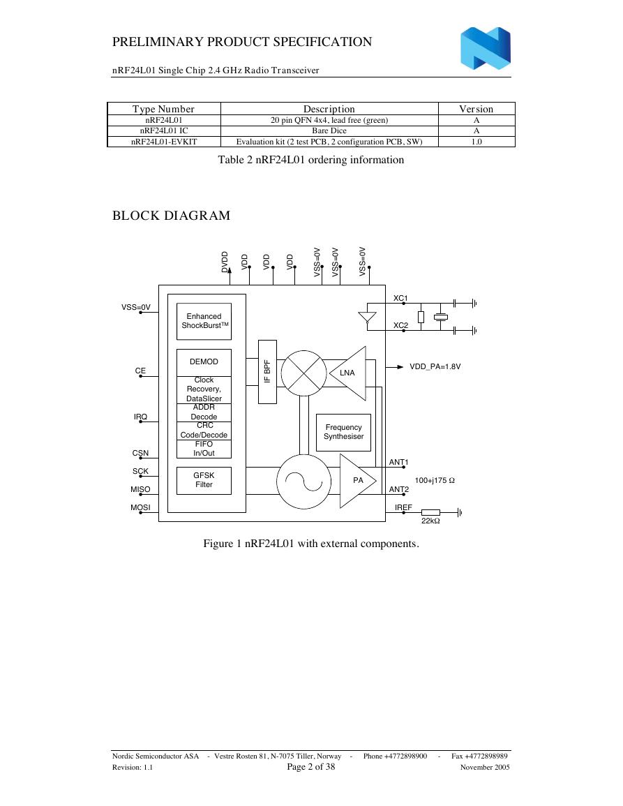
Figure 1 nRF24L01 with external components.
VSS=0V
CE
IRQ
CSN
SCK
MISO
MOSI
Nordic Semiconductor ASA
Revision: 1.1
- Vestre Rosten 81, N-7075 Tiller, Norway
-
Phone +4772898900
-
Page 2 of 38
Fax +4772898989
November 2005
�
PRELIMINARY PRODUCT SPECIFICATION
nRF24L01 Single Chip 2.4 GHz Radio Transceiver
PIN FUNCTIONS
Pin Name
1
2
3
4
5
6
7
8
9
10
11
12
13
14
15
16
17
18
19
20
CE
CSN
SCK
MOSI
MISO
IRQ
VDD
VSS
XC2
XC1
VDD_PA
ANT1
ANT2
VSS
VDD
IREF
VSS
VDD
DVDD
VSS
Pin function Description
Digital Input
Digital Input
Digital Input
Digital Input
Digital Output
Digital Output
Power
Power
Analog Output
Analog Input
Power Output
RF
RF
Power
Power
Analog Input
Power
Power
Power Output
Power
Chip Enable Activates RX or TX mode
SPI Chip Select
SPI Clock
SPI Slave Data Input
SPI Slave Data Output, with tri-state option
Maskable interrupt pin
Power Supply (+3V DC)
Ground (0V)
Crystal Pin 2
Crystal Pin 1
Power Supply (+1.8V) to Power Amplifier
Antenna interface 1
Antenna interface 2
Ground (0V)
Power Supply (+3V DC)
Reference current
Ground (0V)
Power Supply (+3V DC)
Positive Digital Supply output for de-coupling purposes
Ground (0V)
Table 3 nRF24L01 pin function
PIN ASSIGNMENT
VSS
20
DVDD
19
VDD
18
VSS
17
IREF
16
nRF24L01
QFN20 4x4
15
14
13
12
11
VDD
VSS
ANT2
ANT1
VDD_PA
CE
CSN
SCK
MOSI
MISO
1
2
3
4
5
6
IRQ
7
VDD
8
VSS
9
XC2
10
XC1
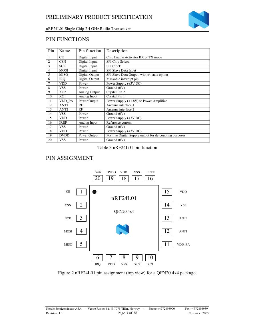
Figure 2 nRF24L01 pin assignment (top view) for a QFN20 4x4 package.
Nordic Semiconductor ASA
Revision: 1.1
- Vestre Rosten 81, N-7075 Tiller, Norway
-
Phone +4772898900
-
Page 3 of 38
Fax +4772898989
November 2005
�
PRELIMINARY PRODUCT SPECIFICATION
nRF24L01 Single Chip 2.4 GHz Radio Transceiver
ELECTRICAL SPECIFICATIONS
Conditions: VDD = +3V, VSS = 0V, TA = - 40ºC to + 85ºC
Symbol Parameter (condition)
Notes Min.
Typ. Max. Units
Operating conditions
Supply voltage
VDD
TEMP Operating Temperature
VIH
VIL
VOH
VOL
fOP
fXTAL
D f1M
D f2M
RGFSK
Digital input pin
HIGH level input voltage
LOW level input voltage
Digital output pin
HIGH level output voltage (IOH=-0.5mA)
LOW level output voltage (IOL=0.5mA)
General RF conditions
Operating frequency
Crystal frequency
Frequency deviation @ 1000kbps
Frequency deviation @ 2000kbps
Data rate ShockBurst™
FCHANNEL Channel spacing @ 1000kbps
FCHANNEL Channel spacing @ 2000kbps
PRF
PRFC
PRFCR
PBW
PRF1
PRF2
IVDD
IVDD
IVDD
IVDD
IVDD
Transmitter operation
Maximum Output Power
RF Power Control Range
RF Power Accuracy
20dB Bandwidth for Modulated Carrier
(2000kbps)
1st Adjacent Channel Transmit Power 2MHz
2nd Adjacent Channel Transmit Power 4MHz
Supply current @ 0dBm output power
Supply current @ -18dBm output power
Average Supply current @ -6dBm output
power, Enhanced ShockBurst™
Supply current in Standby-I mode
Supply current in power down
1
2
3
4
5
1.9
-40
3.0
+27
3.6
+85
0.7VDD
VSS
VDD- 0.3
VSS
2400
>0
16
16
±160
±320
1
2
0
18
11.3
7.0
0.05
32
900
5.25
0.3VDD
VDD
0.3
2525
2000
+4
20
±4
2000
-20
-50
V
ºC
V
V
V
V
MHz
MHz
kHz
kHz
kbps
MHz
MHz
dBm
dB
dB
kHz
dBm
dBm
mA
mA
mA
m A
nA
1 All digital inputs handle up to 5.25V signal inputs. Keep in mind that the VDD of the nRF24L01 must match the
VIH of the driving device for output pins.
2 Usable band is determined by local regulations
3 Antenna load impedance = 100W +j175W
4 Antenna load impedance = 100W +j175W
5 Antenna load impedance = 100W +j175W
. Effective data rate 1000kbps or 2000 kbps
. Effective data rate 10kbps and full packets
Nordic Semiconductor ASA
Revision: 1.1
- Vestre Rosten 81, N-7075 Tiller, Norway
-
Phone +4772898900
-
Page 4 of 38
Fax +4772898989
November 2005
�
PRELIMINARY PRODUCT SPECIFICATION
nRF24L01 Single Chip 2.4 GHz Radio Transceiver
IVDD
IVDD
RXSENS
RXSENS
C/ICO
C/I1ST
C/I2ND
C/I3RD
C/ICO
C/I1ST
C/I2ND
C/I3RD
Receiver operation
Supply current one channel 2000kbps
Supply current one channel 1000kbps
Sensitivity at 0.1%BER (@2000kbps)
Sensitivity at 0.1%BER (@1000kbps)
C/I Co-channel
1st Adjacent Channel Selectivity C/I 2MHz
2nd Adjacent Channel Selectivity C/I 4MHz
3rd Adjacent Channel Selectivity C/I 6MHz
C/I Co-channel
1st Adjacent Channel Selectivity C/I 1MHz
2nd Adjacent Channel Selectivity C/I 2MHz
3rd Adjacent Channel Selectivity C/I 3MHz
6
9
12.3
11.8
-82
-85
57/128
0/5
-21/-19
-27/-27
710/1411
6/10
-22/-20
-30/-25
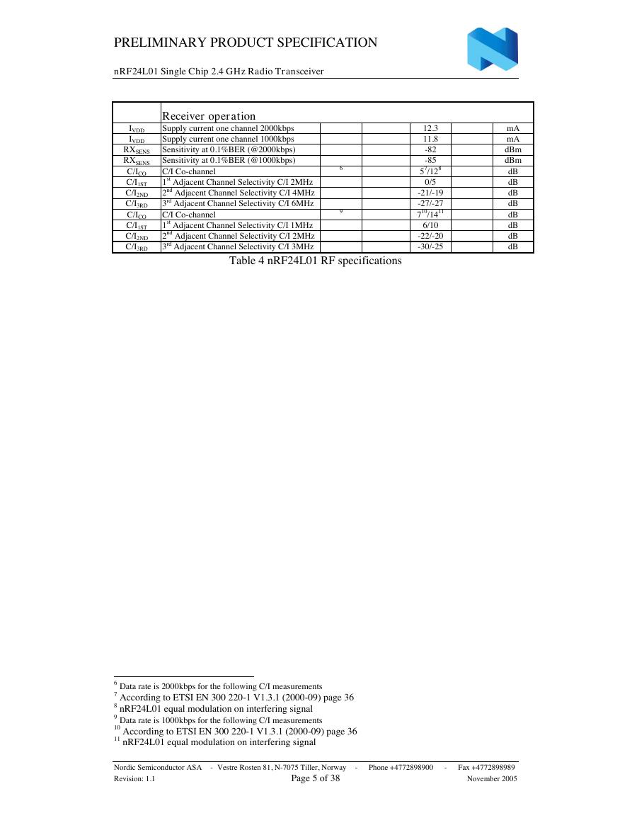
Table 4 nRF24L01 RF specifications
mA
mA
dBm
dBm
dB
dB
dB
dB
dB
dB
dB
dB
6 Data rate is 2000kbps for the following C/I measurements
7 According to ETSI EN 300 220-1 V1.3.1 (2000-09) page 36
8 nRF24L01 equal modulation on interfering signal
9 Data rate is 1000kbps for the following C/I measurements
10 According to ETSI EN 300 220-1 V1.3.1 (2000-09) page 36
11 nRF24L01 equal modulation on interfering signal
Nordic Semiconductor ASA
Revision: 1.1
- Vestre Rosten 81, N-7075 Tiller, Norway
-
Phone +4772898900
-
Page 5 of 38
Fax +4772898989
November 2005
�
PRELIMINARY PRODUCT SPECIFICATION
nRF24L01 Single Chip 2.4 GHz Radio Transceiver
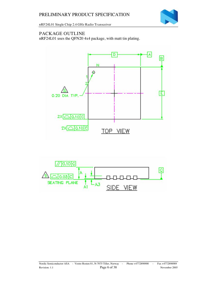
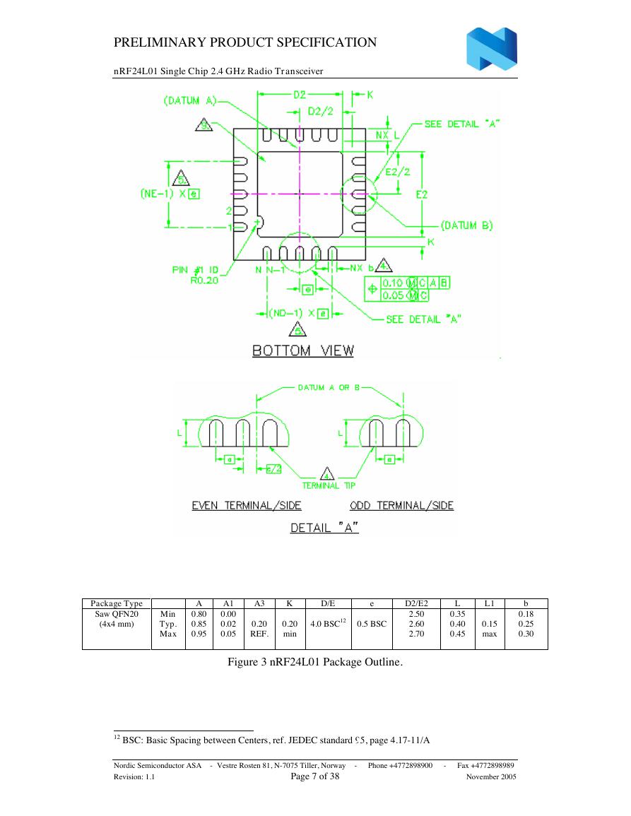
PACKAGE OUTLINE
nRF24L01 uses the QFN20 4x4 package, with matt tin plating.
Nordic Semiconductor ASA
Revision: 1.1
- Vestre Rosten 81, N-7075 Tiller, Norway
-
Phone +4772898900
-
Page 6 of 38
Fax +4772898989
November 2005
�
PRELIMINARY PRODUCT SPECIFICATION
nRF24L01 Single Chip 2.4 GHz Radio Transceiver
Package Type
Saw QFN20
(4x4 mm)
Min
Typ.
Max
A
0.80
0.85
0.95
A1
0.00
0.02
0.05
A3
0.20
REF.
K
0.20
min
D/E
4.0 BSC12
e
0.5 BSC
D2/E2
2.50
2.60
2.70
L
0.35
0.40
0.45
L1
0.15
max
b
0.18
0.25
0.30
Figure 3 nRF24L01 Package Outline.
12 BSC: Basic Spacing between Centers, ref. JEDEC standard 95, page 4.17-11/A
Nordic Semiconductor ASA
Revision: 1.1
- Vestre Rosten 81, N-7075 Tiller, Norway
-
Phone +4772898900
-
Page 7 of 38
Fax +4772898989
November 2005
�
PRELIMINARY PRODUCT SPECIFICATION
nRF24L01 Single Chip 2.4 GHz Radio Transceiver
Package marking:
– Build Code, i.e. unique code for production sites,
package type and test platform
– "X" grade, i.e. Engineering Samples (optional)
– 2 digit Year number
– 2 digit Week number
– 2 letter wafer lot number code
n R F
B X
D D D D D D
Y Y W W L L
Abbreviations:
DDDDDD – Product number, e.g. 24L01
B
X
YY
WW
LL
Absolute Maximum Ratings
Supply voltages
VDD............................- 0.3V to + 3.6V
VSS .................................................. 0V
Input voltage
VI.................................. - 0.3V to 5.25V
Output voltage
VO..................................... VSS to VDD
Total Power Dissipation
PD (TA=85 C) ............................. 60mW
Temperatures
Operating Temperature…. - 40 C to + 85 C
Storage Temperature….… - 40 C to + 125 C
Note: Stress exceeding one or more of the limiting values may cause permanent
damage to the device.
ATTENTION!
Electrostatic Sensitive Device
Observe Precaution for handling.
Nordic Semiconductor ASA
Revision: 1.1
- Vestre Rosten 81, N-7075 Tiller, Norway
-
Phone +4772898900
-
Page 8 of 38
Fax +4772898989
November 2005
�



 V2版本原理图(Capacitive-Fingerprint-Reader-Schematic_V2).pdf
 摄像头工作原理.doc
 VL53L0X简要说明(En.FLVL53L00216).pdf
 原理图(DVK720-Schematic).pdf
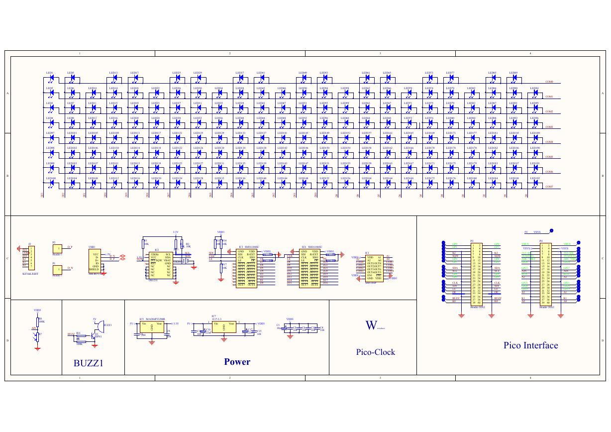 原理图(Pico-Clock-Green-Schdoc).pdf
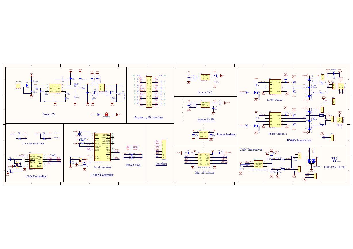 原理图(RS485-CAN-HAT-B-schematic).pdf
 File:SIM7500_SIM7600_SIM7800 Series_SSL_Application Note_V2.00.pdf
 ADS1263(Ads1262).pdf
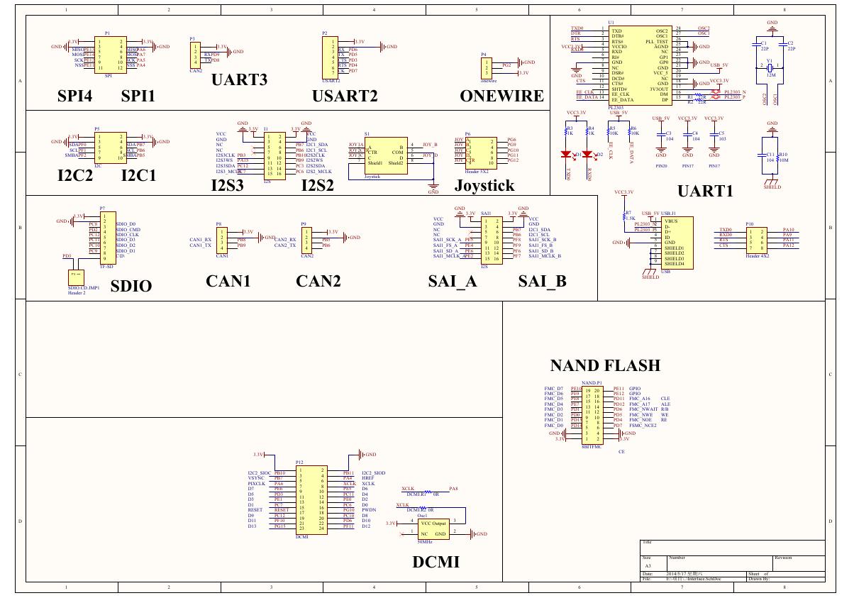 原理图(Open429Z-D-Schematic).pdf
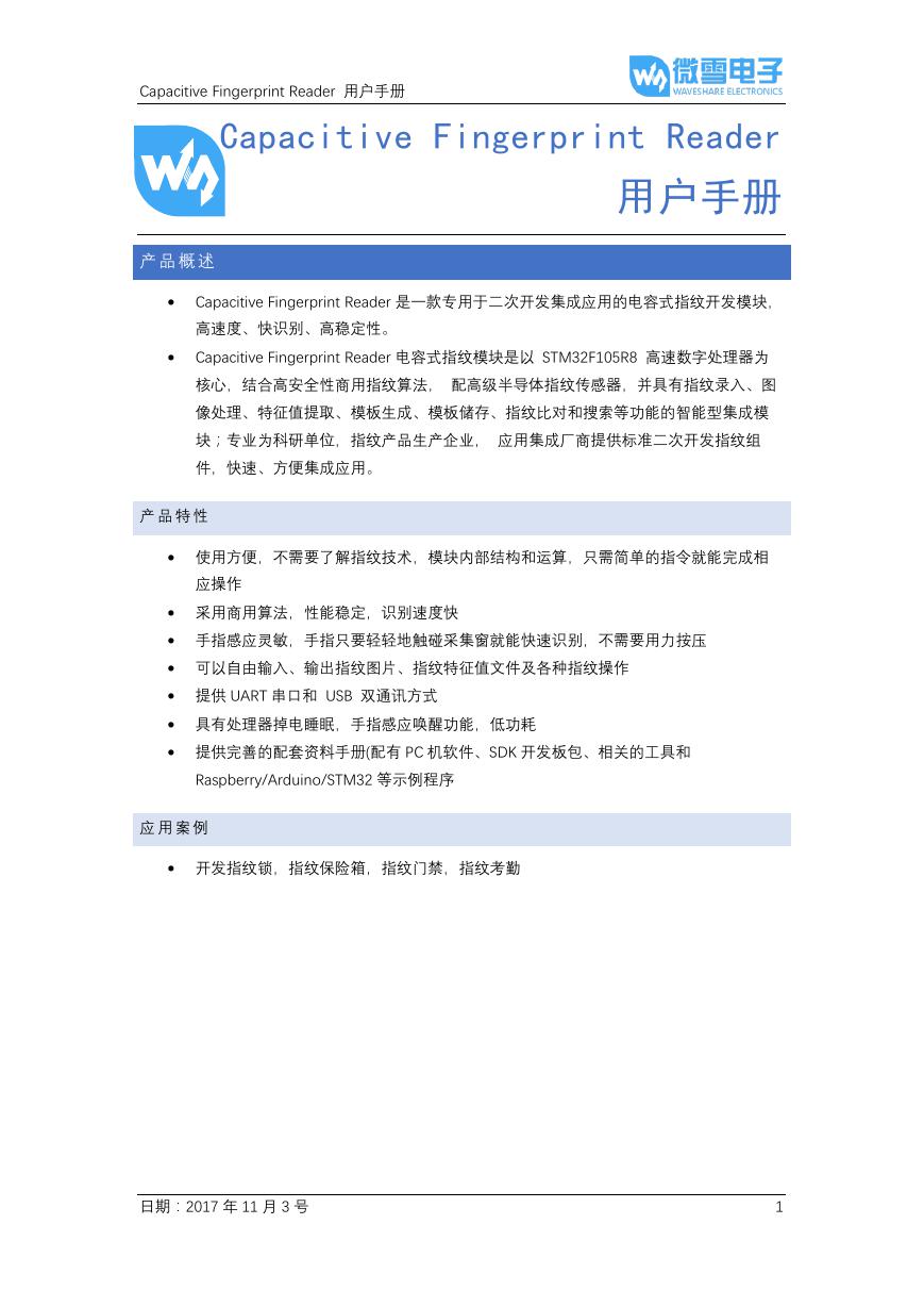 用户手册(Capacitive_Fingerprint_Reader_User_Manual_CN).pdf
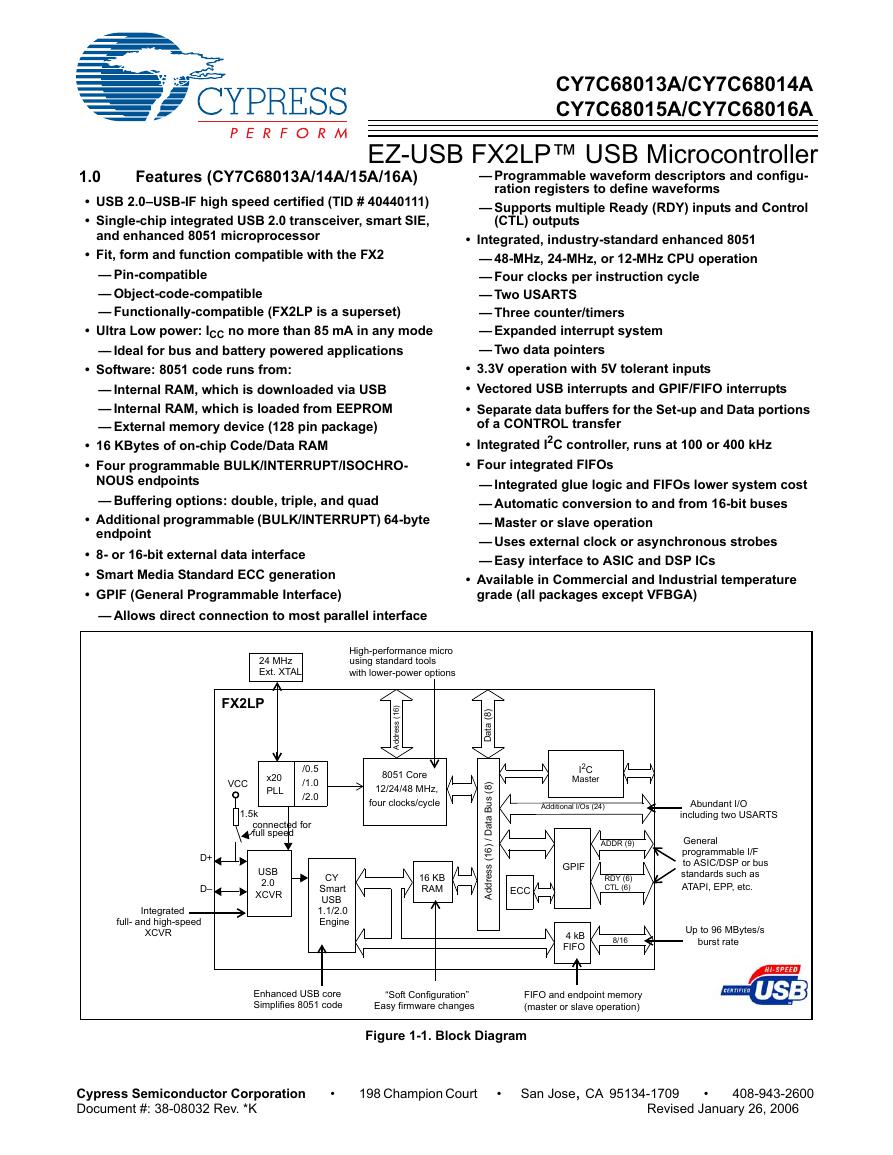 CY7C68013A(英文版)(CY7C68013A).pdf
 TechnicalReference_Dem.pdf