DS3231
Extremely Accurate I2C-Integrated
RTC/TCXO/Crystal
Features
General Description
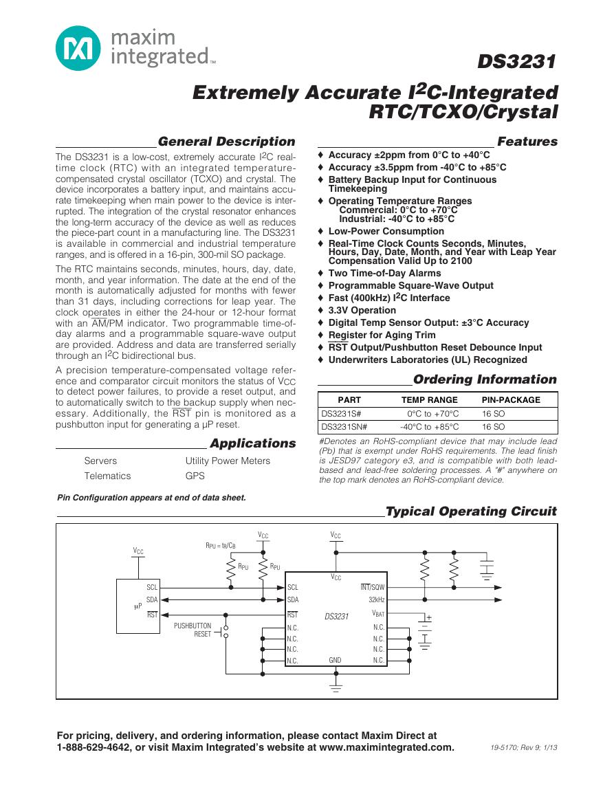
The DS3231 is a low-cost, extremely accurate I2C real-
time clock (RTC) with an integrated temperature-
compensated crystal oscillator (TCXO) and crystal. The
device incorporates a battery input, and maintains accu-
rate timekeeping when main power to the device is inter-
rupted. The integration of the crystal resonator enhances
the long-term accuracy of the device as well as reduces
the piece-part count in a manufacturing line. The DS3231
is available in commercial and industrial temperature
ranges, and is offered in a 16-pin, 300-mil SO package.
The RTC maintains seconds, minutes, hours, day, date,
month, and year information. The date at the end of the
month is automatically adjusted for months with fewer
than 31 days, including corrections for leap year. The
clock operates in either the 24-hour or 12-hour format
with an AM/PM indicator. Two programmable time-of-
day alarms and a programmable square-wave output
are provided. Address and data are transferred serially
through an I2C bidirectional bus.
A precision temperature-compensated voltage refer-
ence and comparator circuit monitors the status of VCC
to detect power failures, to provide a reset output, and
to automatically switch to the backup supply when nec-
essary. Additionally, the RST pin is monitored as a
pushbutton input for generating a µP reset.
Applications
Servers
Telematics
Utility Power Meters
GPS
Pin Configuration appears at end of data sheet.
o Accuracy ±2ppm from 0°C to +40°C
o Accuracy ±3.5ppm from -40°C to +85°C
o Battery Backup Input for Continuous
Timekeeping
o Operating Temperature Ranges
Commercial: 0°C to +70°C
Industrial: -40°C to +85°C
o Low-Power Consumption
o Real-Time Clock Counts Seconds, Minutes,
Hours, Day, Date, Month, and Year with Leap Year
Compensation Valid Up to 2100
o Two Time-of-Day Alarms
o Programmable Square-Wave Output
o Fast (400kHz) I2C Interface
o 3.3V Operation
o Digital Temp Sensor Output: ±3°C Accuracy
o Register for Aging Trim
o RST Output/Pushbutton Reset Debounce Input
o Underwriters Laboratories (UL) Recognized
Ordering Information
TEMP RANGE
0°C to +70°C
-40°C to +85°C
PART
DS3231S#
DS3231SN#
#Denotes an RoHS-compliant device that may include lead
(Pb) that is exempt under RoHS requirements. The lead finish
is JESD97 category e3, and is compatible with both lead-
based and lead-free soldering processes. A "#" anywhere on
the top mark denotes an RoHS-compliant device.
PIN-PACKAGE
16 SO
16 SO
Typical Operating Circuit
VCC
SCL
SDA
RST
µP
VCC
RPU = tR/CB
RPU
RPU
PUSHBUTTON
RESET
VCC
VCC
DS3231
GND
INT/SQW
32kHz
VBAT
N.C.
N.C.
N.C.
N.C.
SCL
SDA
RST
N.C.
N.C.
N.C.
N.C.
For pricing, delivery, and ordering information, please contact Maxim Direct at
1-888-629-4642, or visit Maxim Integrated’s website at www.maximintegrated.com.
19-5170; Rev 9; 1/13
�
DS3231
Extremely Accurate I2C-Integrated
RTC/TCXO/Crystal
ABSOLUTE MAXIMUM RATINGS
Voltage Range on Any Pin Relative to Ground......-0.3V to +6.0V
Junction-to-Ambient Thermal Resistance (θJA) (Note 1)....73°C/W
Junction-to-Case Thermal Resistance (θJC) (Note 1) ......23°C/W
Operating Temperature Range
DS3231S ..............................................................0°C to +70°C
DS3231SN ........................................................-40°C to +85°C
Junction Temperature......................................................+125°C
Storage Temperature Range ...............................-40°C to +85°C
Lead Temperature (soldering, 10s) .................................+260°C
Soldering Temperature (reflow, 2 times max)..................+260°C
(See the Handling,PC Board Layout, and Assemblysection.)
Note 1: Package thermal resistances were obtained using the method described in JEDEC specification JESD51-7, using a four-
layer board. For detailed information on package thermal considerations, refer to www.maxim-ic.com/thermal-tutorial.
Stresses beyond those listed under “Absolute Maximum Ratings” may cause permanent damage to the device. These are stress ratings only, and functional
operation of the device at these or any other conditions beyond those indicated in the operational sections of the specifications is not implied. Exposure to
absolute maximum rating conditions for extended periods may affect device reliability.
RECOMMENDED OPERATING CONDITIONS
(TA = TMIN to TMAX, unless otherwise noted.) (Notes 2, 3)
PARAMETER
SYMBOL
CONDITIONS
Supply Voltage
Logic 1 Input SDA, SCL
Logic 0 Input SDA, SCL
VCC
VBAT
VIH
VIL
TYP
3.3
3.0
MIN
2.3
2.3
0.7 x
VCC
-0.3
MAX
5.5
5.5
VCC +
0.3
0.3 x
VCC
UNITS
V
V
V
V
ELECTRICAL CHARACTERISTICS
(VCC = 2.3V to 5.5V, VCC = Active Supply (see Table 1), TA = TMIN to TMAX, unless otherwise noted.) (Typical values are at VCC =
3.3V, VBAT = 3.0V, and TA = +25°C, unless otherwise noted.) (Notes 2, 3)
PARAMETER
SYMBOL
CONDITIONS
MIN
TYP
Active Supply Current
ICCA
(Notes 4, 5)
2.45
2.575
-1
-1
-200
0
25
MAX
200
300
110
170
575
650
2.70
0.4
0.4
+1
+1
+10
100
UNITS
μA
μA
μA
V
V
V
μA
μA
μA
nA
Maxim Integrated
VCC = 3.63V
VCC = 5.5V
VCC = 3.63V
VCC = 5.5V
I2C bus inactive, 32kHz
output on, SQW output off
(Note 5)
I2C bus inactive, 32kHz
VCC = 3.63V
output on, SQW output off VCC = 5.5V
IOL = 3mA
IOL = 1mA
Output high impedance
RST high impedance (Note 6)
Standby Supply Current
ICCS
Temperature Conversion Current
ICCSCONV
Power-Fail Voltage
Logic 0 Output, 32kHz,
INT/SQW, SDA
Logic 0 Output, RST
Output Leakage Current 32kHz,
INT/SQW, SDA
Input Leakage SCL
RST Pin I/O Leakage
VBAT Leakage Current
(VCC Active)
2
VPF
VOL
VOL
ILO
ILI
IOL
IBATLKG
�
DS3231
Extremely Accurate I2C-Integrated
RTC/TCXO/Crystal
ELECTRICAL CHARACTERISTICS (continued)
(VCC = 2.3V to 5.5V, VCC = Active Supply (see Table 1), TA = TMIN to TMAX, unless otherwise noted.) (Typical values are at VCC =
3.3V, VBAT = 3.0V, and TA = +25°C, unless otherwise noted.) (Notes 2, 3)
PARAMETER
SYMBOL
CONDITIONS
MIN
Output Frequency
fOUT
VCC = 3.3V or VBAT = 3.3V
Frequency Stability vs.
Temperature (Commercial)
Frequency Stability vs.
Temperature (Industrial)
f/fOUT
f/fOUT
VCC = 3.3V or
VBAT = 3.3V,
aging offset = 00h
VCC = 3.3V or
VBAT = 3.3V,
aging offset = 00h
0°C to +40°C
>40°C to +70°C
-40°C to <0°C
0°C to +40°C
>40°C to +85°C
Frequency Stability vs. Voltage
f/V
Trim Register Frequency
Sensitivity per LSB
f/LSB
Specified at:
-40°C
+25°C
+70°C
+85°C
Temperature Accuracy
Crystal Aging
Temp
f/fO
VCC = 3.3V or VBAT = 3.3V
After reflow,
not production tested
First year
0–10 years
-3
TYP
32.768
1
0.7
0.1
0.4
0.8
UNITS
kHz
ppm
ppm
ppm/V
ppm
MAX
±2
±3.5
±3.5
±2
±3.5
+3
°C
±1.0
±5.0
ppm
ELECTRICAL CHARACTERISTICS
(VCC = 0V, VBAT = 2.3V to 5.5V, TA = TMIN to TMAX, unless otherwise noted.) (Note 2)
PARAMETER
SYMBOL
CONDITIONS
MIN
TYP
Active Battery Current
IBATA
EOSC = 0, BBSQW = 0,
SCL = 400kHz (Note 5)
VBAT = 3.63V
VBAT = 5.5V
MAX
70
150
Timekeeping Battery Current
IBATT
Temperature Conversion Current
IBATTC
Data-Retention Current
IBATTDR
EOSC = 0, BBSQW = 0,
EN32kHz = 1,
SCL = SDA = 0V or
SCL = SDA = VBAT (Note 5) VBAT = 5.5V
VBAT = 3.63V
EOSC = 0, BBSQW = 0,
SCL = SDA = 0V or
SCL = SDA = VBAT
EOSC = 1, SCL = SDA = 0V, +25°C
VBAT = 3.63V
VBAT = 5.5V
0.84
3.0
1.0
3.5
575
650
100
UNITS
μA
μA
μA
nA
Maxim Integrated
3
�
DS3231
Extremely Accurate I2C-Integrated
RTC/TCXO/Crystal
AC ELECTRICAL CHARACTERISTICS
(VCC = VCC(MIN) to VCC(MAX) or VBAT = VBAT(MIN) to VBAT(MAX), VBAT > VCC, TA = TMIN to TMAX, unless otherwise noted.) (Note 2)
PARAMETER
SYMBOL
CONDITIONS
SCL Clock Frequency
Bus Free Time Between STOP
and START Conditions
Hold Time (Repeated) START
Condition (Note 7)
Low Period of SCL Clock
High Period of SCL Clock
Data Hold Time (Notes 8, 9)
Data Setup Time (Note 10)
START Setup Time
Rise Time of Both SDA and SCL
Signals (Note 11)
Fall Time of Both SDA and SCL
Signals (Note 11)
fSCL
tBUF
tHD:STA
tLOW
tHIGH
tHD:DAT
tSU:DAT
tSU:STA
tR
tF
Setup Time for STOP Condition
tSU:STO
Capacitive Load for Each Bus
Line
Capacitance for SDA, SCL
Pulse Width of Spikes That Must
Be Suppressed by the Input Filter
Pushbutton Debounce
Reset Active Time
Oscillator Stop Flag (OSF) Delay
Temperature Conversion Time
CB
CI/O
tSP
PBDB
tRST
tOSF
tCONV
Fast mode
Standard mode
Fast mode
Standard mode
Fast mode
Standard mode
Fast mode
Standard mode
Fast mode
Standard mode
Fast mode
Standard mode
Fast mode
Standard mode
Fast mode
Standard mode
Fast mode
Standard mode
Fast mode
Standard mode
Fast mode
Standard mode
(Note 11)
(Note 12)
POWER-SWITCH CHARACTERISTICS
(TA = TMIN to TMAX)
MIN
100
0
1.3
4.7
0.6
4.0
1.3
4.7
0.6
4.0
0
0
100
250
0.6
4.7
20 +
0.1CB
20 +
0.1CB
0.6
4.7
TYP
10
30
250
250
100
125
MAX
400
100
UNITS
kHz
0.9
0.9
300
1000
300
300
400
200
μs
μs
μs
μs
μs
ns
μs
ns
ns
μs
pF
pF
ns
ms
ms
ms
ms
PARAMETER
SYMBOL
CONDITIONS
MIN
TYP
MAX
UNITS
VCC Fall Time; VPF(MAX) to
VPF(MIN)
VCC Rise Time; VPF(MIN) to
VPF(MAX)
Recovery at Power-Up
tVCCF
tVCCR
tREC
(Note 13)
300
0
250
300
μs
μs
ms
4
Maxim Integrated
�
DS3231
Extremely Accurate I2C-Integrated
RTC/TCXO/Crystal
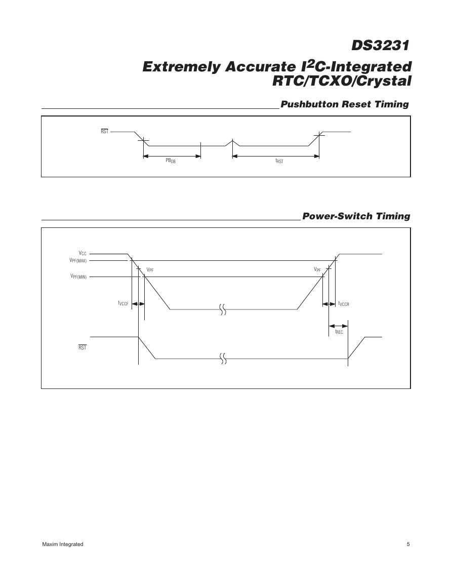
Pushbutton Reset Timing
RST
PBDB
tRST
Power-Switch Timing
VCC
VPF(MAX)
VPF(MIN)
RST
tVCCF
VPF
VPF
tVCCR
tREC
Maxim Integrated
5
�
DS3231
Extremely Accurate I2C-Integrated
RTC/TCXO/Crystal
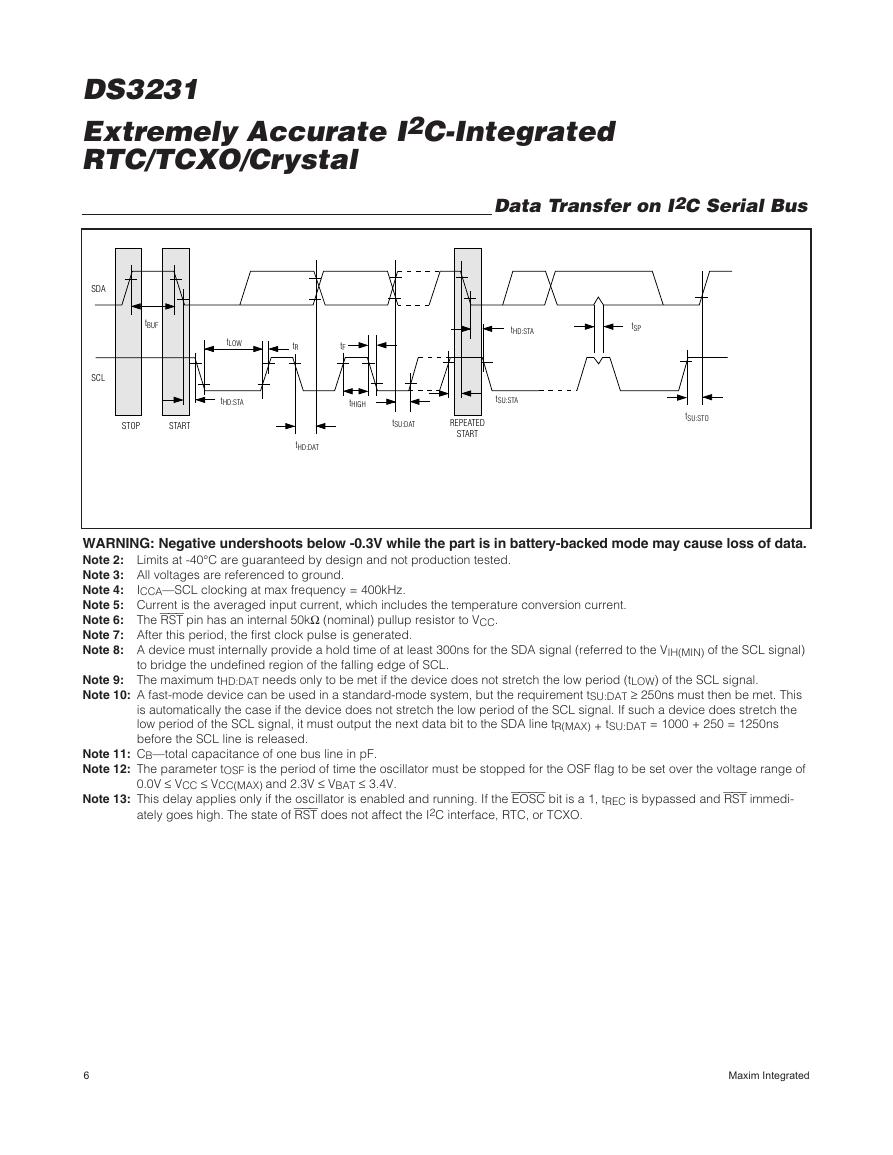
Data Transfer on I2C Serial Bus
SDA
SCL
tBUF
tLOW
tR
tF
tHD:STA
tSP
tHD:STA
tHIGH
tSU:STA
STOP
START
tSU:DAT
REPEATED
START
tHD:DAT
tSU:STO
WARNING: Negative undershoots below -0.3V while the part is in battery-backed mode may cause loss of data.
Note 2: Limits at -40°C are guaranteed by design and not production tested.
Note 3: All voltages are referenced to ground.
Note 4:
Note 5: Current is the averaged input current, which includes the temperature conversion current.
Note 6: The RST pin has an internal 50kΩ (nominal) pullup resistor to VCC.
Note 7: After this period, the first clock pulse is generated.
Note 8: A device must internally provide a hold time of at least 300ns for the SDA signal (referred to the VIH(MIN) of the SCL signal)
ICCA—SCL clocking at max frequency = 400kHz.
to bridge the undefined region of the falling edge of SCL.
Note 9: The maximum tHD:DAT needs only to be met if the device does not stretch the low period (tLOW) of the SCL signal.
Note 10: A fast-mode device can be used in a standard-mode system, but the requirement tSU:DAT ≥ 250ns must then be met. This
is automatically the case if the device does not stretch the low period of the SCL signal. If such a device does stretch the
low period of the SCL signal, it must output the next data bit to the SDA line tR(MAX) + tSU:DAT = 1000 + 250 = 1250ns
before the SCL line is released.
Note 11: CB—total capacitance of one bus line in pF.
Note 12: The parameter tOSF is the period of time the oscillator must be stopped for the OSF flag to be set over the voltage range of
0.0V ≤ VCC ≤ VCC(MAX) and 2.3V ≤ VBAT ≤ 3.4V.
Note 13: This delay applies only if the oscillator is enabled and running. If the EOSC bit is a 1, tREC is bypassed and RST immedi-
ately goes high. The state of RST does not affect the I2C interface, RTC, or TCXO.
6
Maxim Integrated
�
DS3231
Extremely Accurate I2C-Integrated
RTC/TCXO/Crystal
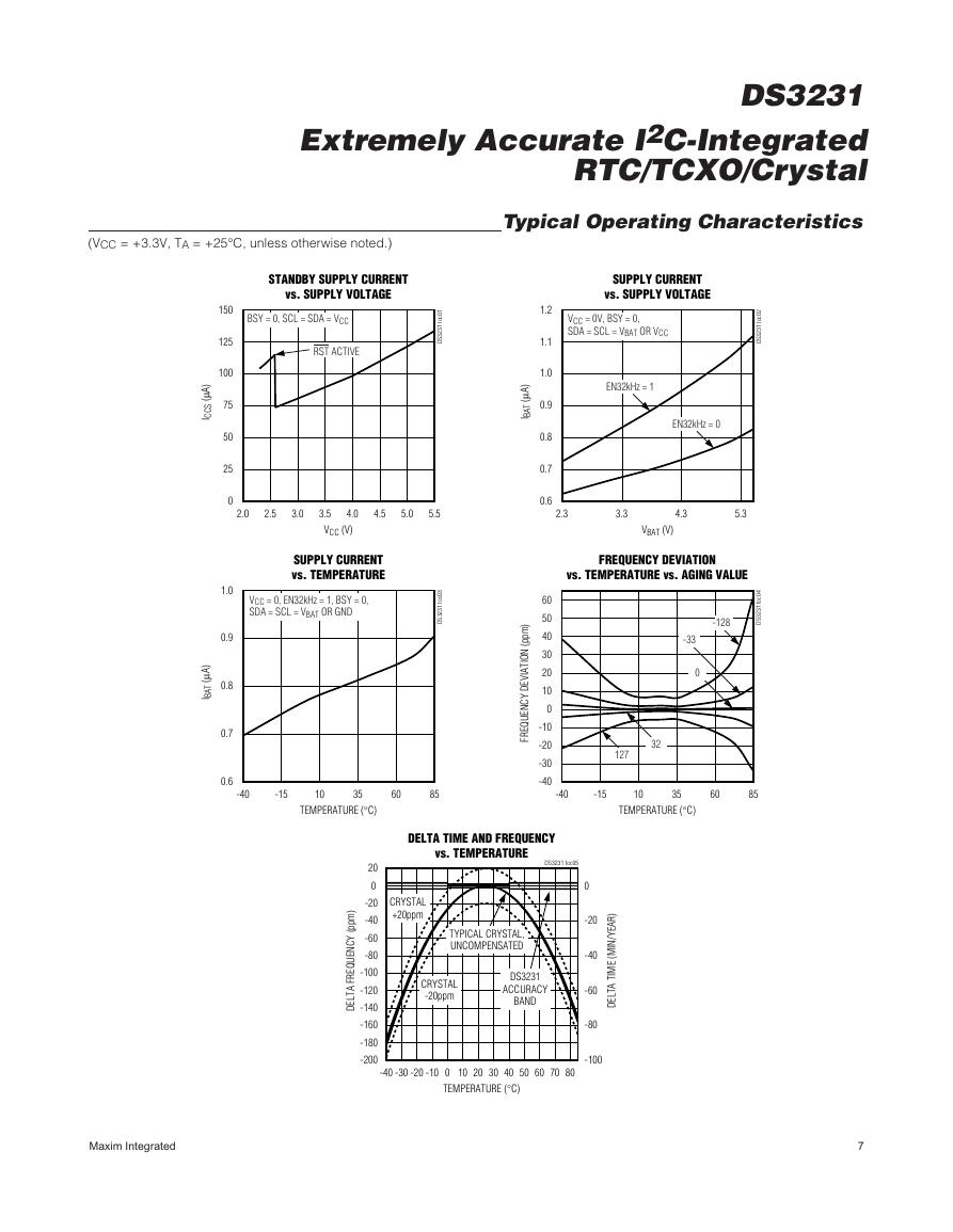
Typical Operating Characteristics
(VCC = +3.3V, TA = +25°C, unless otherwise noted.)
)
A
μ
(
S
C
C
I
)
A
μ
(
T
A
B
I
150
125
100
75
50
25
0
1.0
0.9
0.8
0.7
0.6
STANDBY SUPPLY CURRENT
vs. SUPPLY VOLTAGE
BSY = 0, SCL = SDA = VCC
RST ACTIVE
1
0
c
o
t
1
3
2
3
S
D
2.0
2.5
3.0
4.0
3.5
VCC (V)
4.5
5.0
5.5
SUPPLY CURRENT
vs. TEMPERATURE
VCC = 0, EN32kHz = 1, BSY = 0,
SDA = SCL = VBAT OR GND
3
0
c
o
t
1
3
2
3
S
D
-40
-15
10
35
60
85
TEMPERATURE (°C)
1.2
1.1
1.0
0.9
0.8
0.7
0.6
60
50
40
30
20
10
0
-10
-20
-30
-40
SUPPLY CURRENT
vs. SUPPLY VOLTAGE
VCC = 0V, BSY = 0,
SDA = SCL = VBAT OR VCC
2
0
c
o
t
1
3
2
3
S
D
EN32kHz = 1
EN32kHz = 0
2.3
3.3
4.3
5.3
VBAT (V)
FREQUENCY DEVIATION
vs. TEMPERATURE vs. AGING VALUE
4
0
c
o
t
1
3
2
3
S
D
-128
-33
0
32
127
-40
-15
10
35
60
85
TEMPERATURE (°C)
)
A
μ
(
T
A
B
I
)
m
p
p
(
I
I
N
O
T
A
V
E
D
Y
C
N
E
U
Q
E
R
F
)
m
p
p
(
Y
C
N
E
U
Q
E
R
F
A
T
L
E
D
20
0
-20
-40
-60
-80
-100
-120
-140
-160
-180
-200
DELTA TIME AND FREQUENCY
vs. TEMPERATURE
DS3231 toc05
CRYSTAL
+20ppm
TYPICAL CRYSTAL,
UNCOMPENSATED
CRYSTAL
-20ppm
DS3231
ACCURACY
BAND
-40
-30 -20
-10 0 10 20 30 40
TEMPERATURE (°C)
50 60
70
80
)
R
A
E
Y
/
I
N
M
(
E
M
I
T
A
T
L
E
D
0
-20
-40
-60
-80
-100
Maxim Integrated
7
�
DS3231
Extremely Accurate I2C-Integrated
RTC/TCXO/Crystal
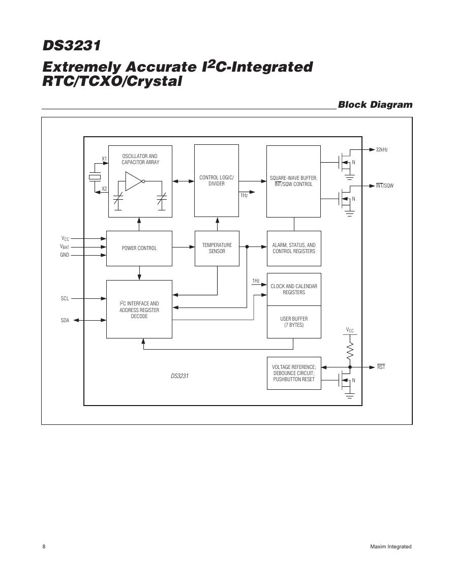
OSCILLATOR AND
CAPACITOR ARRAY
X1
X2
CONTROL LOGIC/
DIVIDER
SQUARE-WAVE BUFFER;
INT/SQW CONTROL
1Hz
VCC
VBAT
GND
SCL
SDA
POWER CONTROL
TEMPERATURE
SENSOR
ALARM, STATUS, AND
CONTROL REGISTERS
I2C INTERFACE AND
ADDRESS REGISTER
DECODE
DS3231
1Hz
CLOCK AND CALENDAR
REGISTERS
USER BUFFER
(7 BYTES)
VOLTAGE REFERENCE;
DEBOUNCE CIRCUIT;
PUSHBUTTON RESET
Block Diagram
32kHz
INT/SQW
RST
N
N
VCC
N
8
Maxim Integrated
�


 V2版本原理图(Capacitive-Fingerprint-Reader-Schematic_V2).pdf
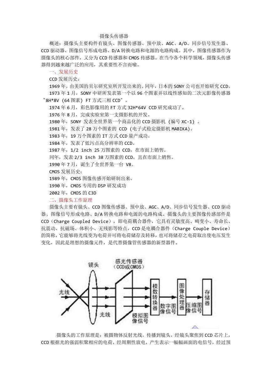 摄像头工作原理.doc
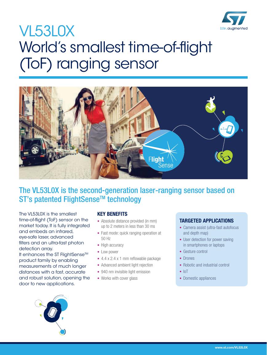 VL53L0X简要说明(En.FLVL53L00216).pdf
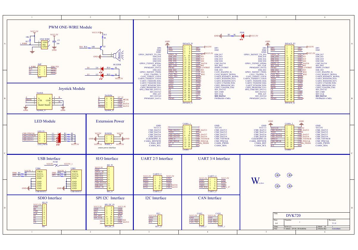 原理图(DVK720-Schematic).pdf
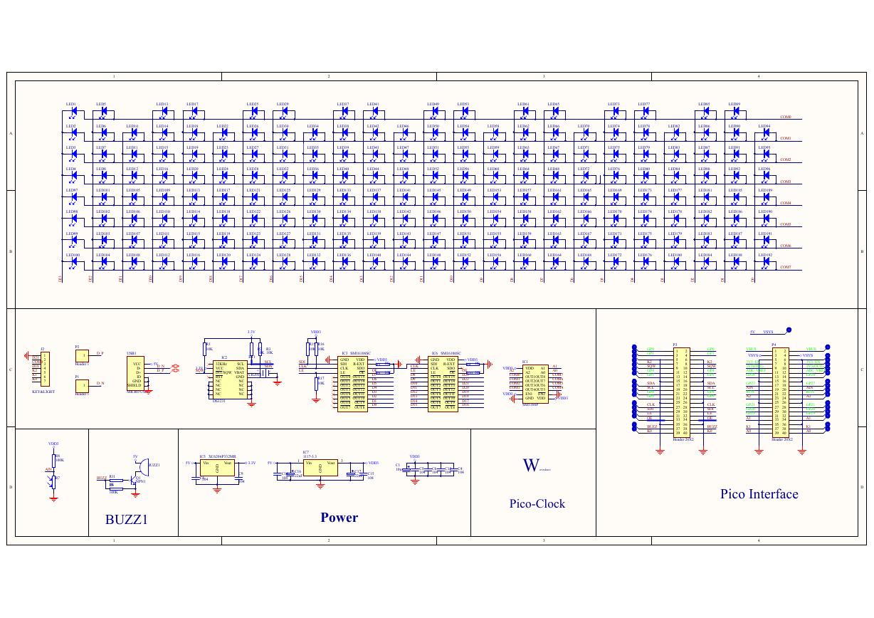 原理图(Pico-Clock-Green-Schdoc).pdf
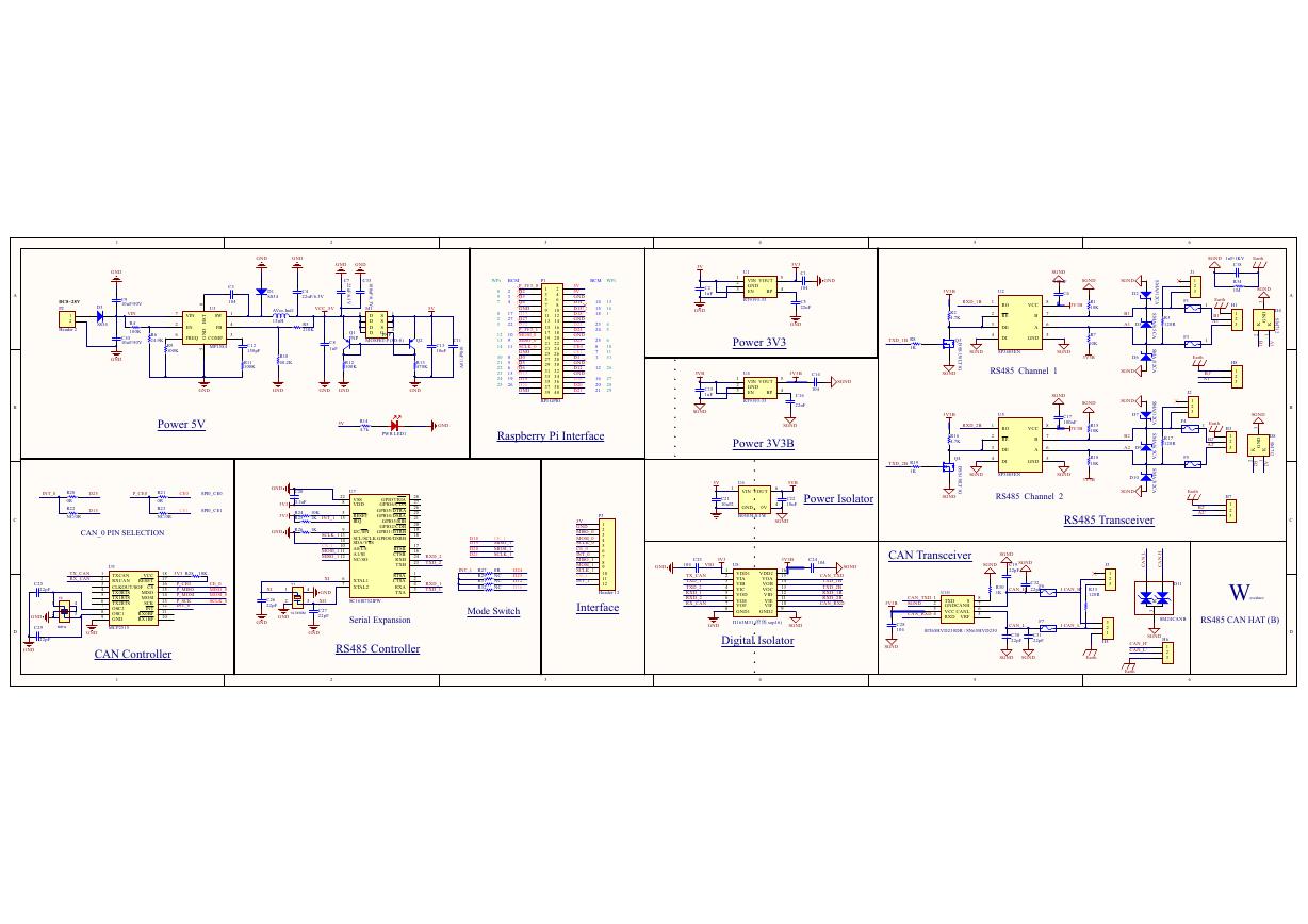 原理图(RS485-CAN-HAT-B-schematic).pdf
 File:SIM7500_SIM7600_SIM7800 Series_SSL_Application Note_V2.00.pdf
 ADS1263(Ads1262).pdf
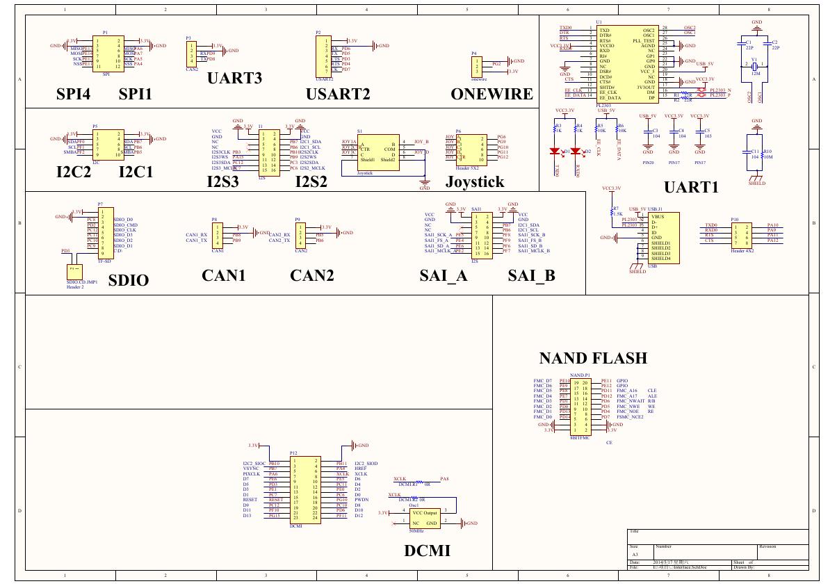 原理图(Open429Z-D-Schematic).pdf
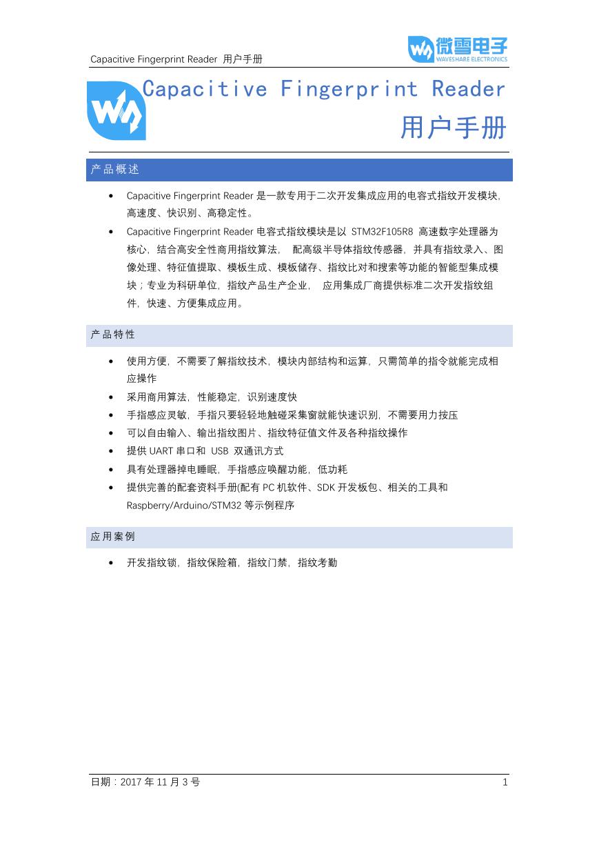 用户手册(Capacitive_Fingerprint_Reader_User_Manual_CN).pdf
 CY7C68013A(英文版)(CY7C68013A).pdf
 TechnicalReference_Dem.pdf