INTRODUCTION
FT5x06
True Multi-Touch
Capacitive Touch Panel Controller
The FT5x06 Series ICs are single-chip capacitive touch panel controller ICs with a built-in 8 bit Micro-controller unit (MCU).They
adopt the mutual capacitance approach, which supports true multi-touch capability. In conjunction with a mutual capacitive touch
panel, the FT5x06 have user-friendly input functions, which can be applied on many portable devices, such as cellular phones, MIDs,
netbook and notebook personal computers.
The FT5x06 series ICs include FT5206/FT5306/FT5406, the difference of their specifications will be listed individually in this
datasheet.
FEATURES
Mutual Capacitive Sensing Techniques
True Multi-touch with up to 10 Points of Absolution X and
Y Coordinates
Immune to RF Interferences
Auto-calibration: Insensitive to Capacitance and Environ-
mental Variations
Supports up to 28 Transmit Lines and 16 Receive Lines
Supports up to 8” Touch Screen
Full Programmable Scan Sequences with Individual Ad-
justable Receive Lines and Transmit Lines to Support
Various Applications
High Report Rate: More than 100Hz
Touch Resolution of 100 Dots per Inch (dpi) or above --
depending on the Panel Size
Optional Interfaces :I2C/SPI
2.8V to 3.6V Operating Voltage
Supports 1.8V/AVDD IOVCC
Capable of Driving Single Channel (transmit/receive) Re-
Capable of Supporting Single Channel (transmit/receive)
sistance: Up to15K Ω
Capacitance: 60 pF
Optimal Sensing Mutual Capacitor: 1pF~4pF
12-Bit ADC Accuracy
Built-in MCU with 28KB Program Memory, 6KB Data
Memory and 256B Internal Data Space
11 Internal Interrupt Sources and 2 External Interrupt
Sources
3 Operating Modes
Active
Monitor
Hibernate
Operating Temperature Range: -20°C to +85°C
FocalTech Systems Co., Ltd · www.focaltech-systems.com · support@focaltech-systems.com
Document Number: D-FT5x06-1212-V4.0 (Version: 4.0) Revised Dec. 18, 2012
From No.: F-OI-RD01-03-03-B
�
FT5x06
DATASHEET
1.1
2
TABLE OF CONTENTS
\\
INTRODUCTION..................................................................................................................................................... I
FEATURES ............................................................................................................................................................... I
1
OVERVIEW ......................................................................................................................................................... 1
TYPICAL APPLICATIONS ................................................................................................................................... 1
FUNCTIONAL DESCRIPTION .............................................................................................................................. 1
2.1 MCU ........................................................................................................................................................... 2
OPERATION MODES ........................................................................................................................................ 2
2.2
HOST INTERFACE............................................................................................................................................ 3
2.3
SERIAL INTERFACE ......................................................................................................................................... 3
2.4
2.4.1
I2C ..................................................................................................................................................... 3
2.4.2 SPI ..................................................................................................................................................... 4
ELECTRICAL SPECIFICATIONS ........................................................................................................................................... 8
ABSOLUTE MAXIMUM RATINGS ...................................................................................................................................... 8
DC CHARACTERISTICS ............................................................................................................................................... 9
AC CHARACTERISTICS ............................................................................................................................................... 9
I/OPORTSCIRCUITS ................................................................................................................................................10
POWER ON/RESET/WAKE SEQUENCE ..............................................................................................................................11
PIN CONFIGURATIONS ..................................................................................................................................................12
PACKAGE INFORMATION ...............................................................................................................................................15
PACKAGE INFORMATION OF QFN-5X5-40L PACKAGE .................................................................................................................15
PACKAGE INFORMATION OF QFN-6X6-48L PACKAGE .................................................................................................................16
PACKAGE INFORMATION OF QFN-6X6-56L PACKAGE ..................................................................................................................17
PACKAGE INFORMATION OF QFN-8X8-68L PACKAGE ..................................................................................................................18
ORDER INFORMATION ...............................................................................................................................................19
3.1
3.2
3.3
3.4
3.5
5.1
5.2
5.3
5.4
5.5
3
4
5
FocalTech Systems Co., Ltd · www.focaltech-systems.com · support@focaltech-systems.com
Document Number: D-FT5x06-1212-V4.0 (Version: 4.0) Revised Dec. 18, 2012
From No.: F-OI-RD01-03-03-B
�
OVERVIEW
Typical Applications
1
1.1
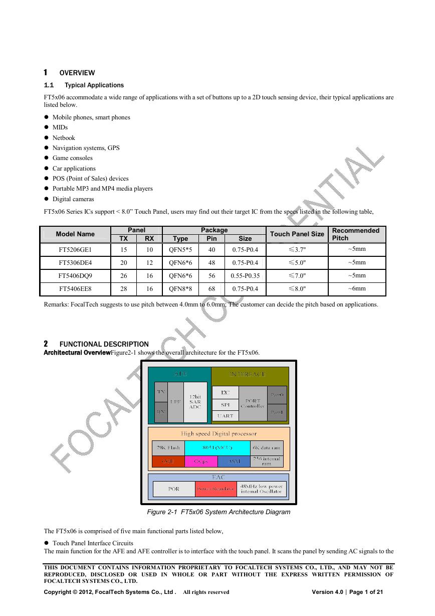
FT5x06 accommodate a wide range of applications with a set of buttons up to a 2D touch sensing device, their typical applications are
listed below.
Mobile phones, smart phones
MIDs
Netbook
Navigation systems, GPS
Game consoles
Car applications
POS (Point of Sales) devices
Portable MP3 and MP4 media players
Digital cameras
FT5x06 Series ICs support < 8.0” Touch Panel, users may find out their target IC from the specs listed in the following table,
Model Name
FT5206GE1
FT5306DE4
FT5406DQ9
FT5406EE8
Panel
TX
15
RX
10
20
26
28
12
16
16
Type
QFN5*5
QFN6*6
QFN6*6
QFN8*8
Package
Pin
40
48
56
68
Size
0.75-P0.4
0.75-P0.4
0.55-P0.35
0.75-P0.4
Touch Panel Size Recommended
Pitch
≤3.7"
≤5.0"
≤7.0"
≤8.0"
~5mm
~5mm
~5mm
~6mm
Remarks: FocalTech suggests to use pitch between 4.0mm to 6.0mm; The customer can decide the pitch based on applications.
FUNCTIONAL DESCRIPTION
2
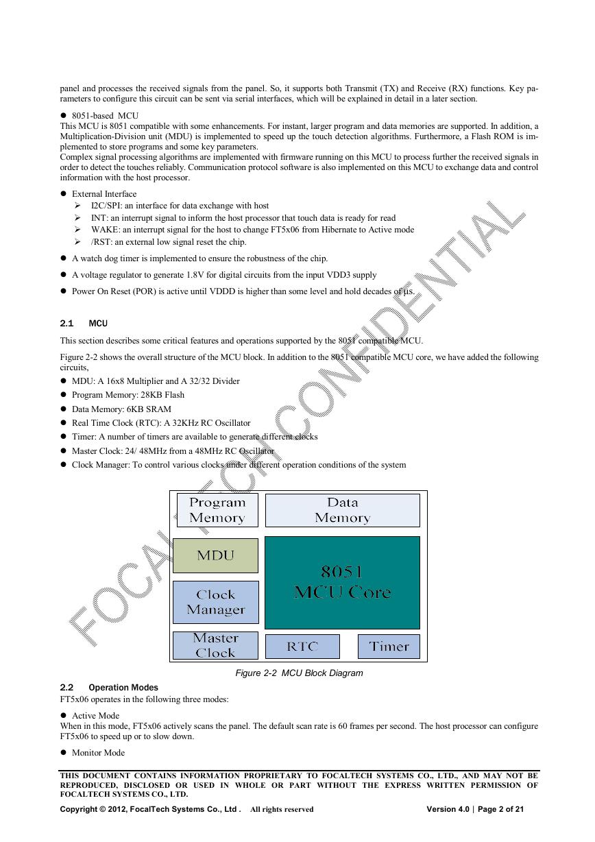
Architectural OverviewFigure2-1 shows the overall architecture for the FT5x06.
Figure 2-1 FT5x06 System Architecture Diagram
The FT5x06 is comprised of five main functional parts listed below,
Touch Panel Interface Circuits
The main function for the AFE and AFE controller is to interface with the touch panel. It scans the panel by sending AC signals to the
THIS DOCUMENT CONTAINS INFORMATION PROPRIETARY TO FOCALTECH SYSTEMS CO., LTD., AND MAY NOT BE
REPRODUCED, DISCLOSED OR USED IN WHOLE OR PART WITHOUT THE EXPRESS WRITTEN PERMISSION OF
FOCALTECH SYSTEMS CO., LTD.
Copyright © 2012, FocalTech Systems Co., Ltd . All rights reserved Version 4.0︱Page 1 of 21
�
panel and processes the received signals from the panel. So, it supports both Transmit (TX) and Receive (RX) functions. Key pa-
rameters to configure this circuit can be sent via serial interfaces, which will be explained in detail in a later section.
8051-based MCU
This MCU is 8051 compatible with some enhancements. For instant, larger program and data memories are supported. In addition, a
Multiplication-Division unit (MDU) is implemented to speed up the touch detection algorithms. Furthermore, a Flash ROM is im-
plemented to store programs and some key parameters.
Complex signal processing algorithms are implemented with firmware running on this MCU to process further the received signals in
order to detect the touches reliably. Communication protocol software is also implemented on this MCU to exchange data and control
information with the host processor.
External Interface
I2C/SPI: an interface for data exchange with host
INT: an interrupt signal to inform the host processor that touch data is ready for read
WAKE: an interrupt signal for the host to change FT5x06 from Hibernate to Active mode
/RST: an external low signal reset the chip.
A watch dog timer is implemented to ensure the robustness of the chip.
A voltage regulator to generate 1.8V for digital circuits from the input VDD3 supply
Power On Reset (POR) is active until VDDD is higher than some level and hold decades of μs.
2.1 MCU
This section describes some critical features and operations supported by the 8051 compatible MCU.
Figure 2-2 shows the overall structure of the MCU block. In addition to the 8051 compatible MCU core, we have added the following
circuits,
MDU: A 16x8 Multiplier and A 32/32 Divider
Program Memory: 28KB Flash
Data Memory: 6KB SRAM
Real Time Clock (RTC): A 32KHz RC Oscillator
Timer: A number of timers are available to generate different clocks
Master Clock: 24/ 48MHz from a 48MHz RC Oscillator
Clock Manager: To control various clocks under different operation conditions of the system
Figure 2-2 MCU Block Diagram
Operation Modes
2.2
FT5x06 operates in the following three modes:
Active Mode
When in this mode, FT5x06 actively scans the panel. The default scan rate is 60 frames per second. The host processor can configure
FT5x06 to speed up or to slow down.
Monitor Mode
THIS DOCUMENT CONTAINS INFORMATION PROPRIETARY TO FOCALTECH SYSTEMS CO., LTD., AND MAY NOT BE
REPRODUCED, DISCLOSED OR USED IN WHOLE OR PART WITHOUT THE EXPRESS WRITTEN PERMISSION OF
FOCALTECH SYSTEMS CO., LTD.
Copyright © 2012, FocalTech Systems Co., Ltd . All rights reserved Version 4.0︱Page 2 of 21
�
When in this mode, FT5x06 scans the panel at a reduced speed. The default scan rate is 25 frames per second and the host processor
can increase or decrease this rate. When in this mode, most algorithms are stopped. A simpler algorithm is being executed to determine
if there is a touch or not. When a touch is detected, FT5x06 shall enter the Active mode immediately to acquire the touch information
quickly. During this mode, the serial port is closed and no data shall be transferred with the host processor.
Hibernate Mode
In this mode, the chip is set in a power down mode. It shall only respond to the “WAKE” or “RESET” signal from the host processor.
The chip therefore consumes very little current, which help prolong the standby time for the portable devices.
2.3
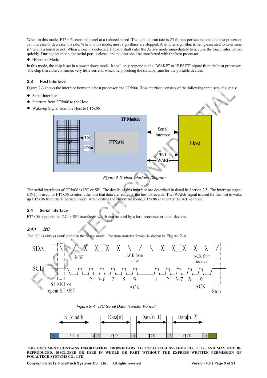
Figure 2-3 shows the interface between a host processor and FT5x06. This interface consists of the following three sets of signals:
Serial Interface
Interrupt from FT5x06 to the Host
Wake-up Signal from the Host to FT5x06
Host Interface
TP Module
TP
TX
RX
FT5x06
Serial
Interface
/INT
/WAKE
Host
Figure 2-3 Host Interface Diagram
The serial interfaces of FT5x06 is I2C or SPI. The details of this interface are described in detail in Section 2.5. The interrupt signal
(/INT) is used for FT5x06 to inform the host that data are ready for the host to receive. The /WAKE signal is used for the host to wake
up FT5x06 from the Hibernate mode. After exiting the Hibernate mode, FT5x06 shall enter the Active mode.
2.4
FT5x06 supports the I2C or SPI interfaces, which can be used by a host processor or other devices.
Serial Interface
I2C
2.4.1
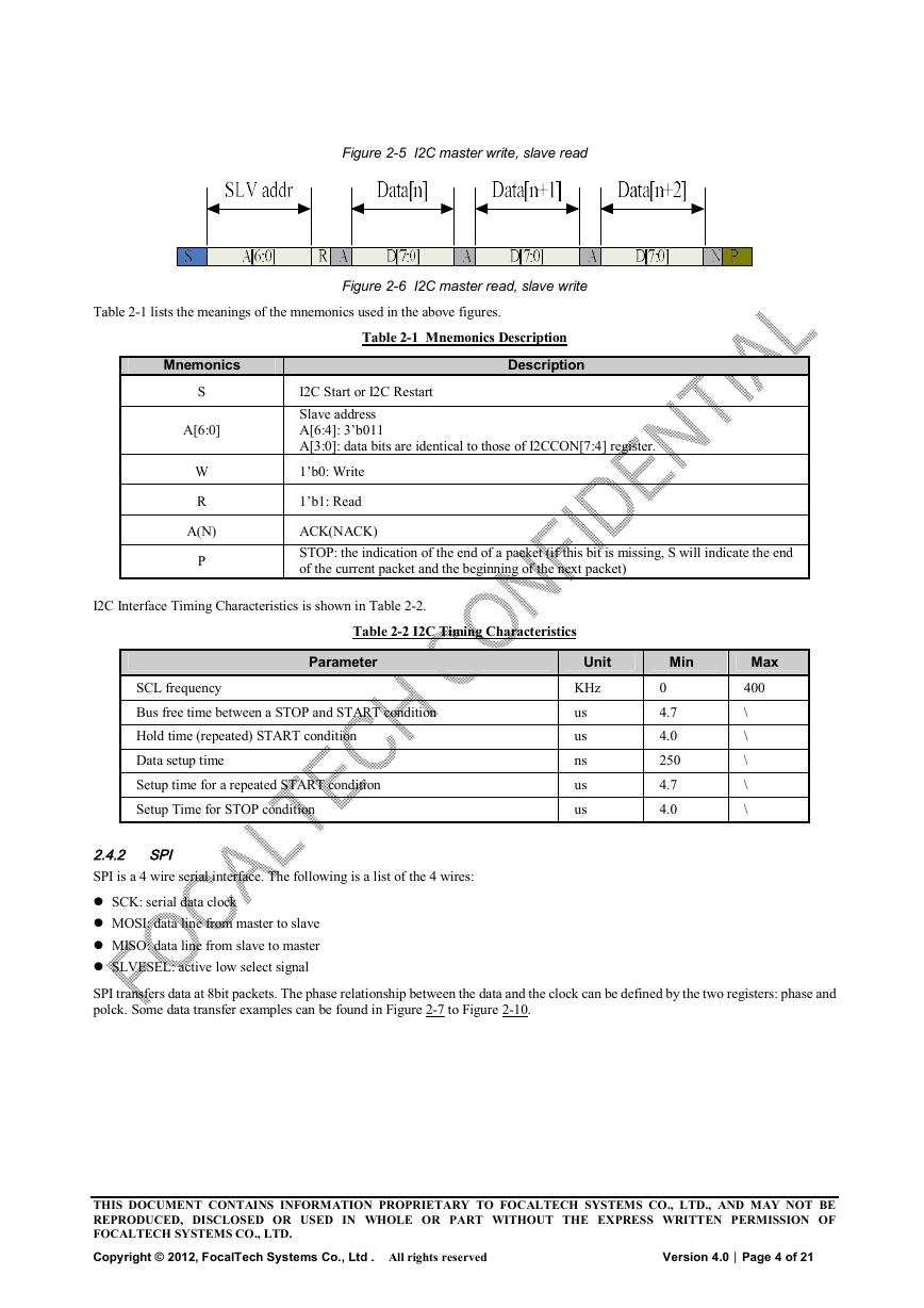
The I2C is always configured in the Slave mode. The data transfer format is shown in Figure 2-4.
Figure 2-4 I2C Serial Data Transfer Format
THIS DOCUMENT CONTAINS INFORMATION PROPRIETARY TO FOCALTECH SYSTEMS CO., LTD., AND MAY NOT BE
REPRODUCED, DISCLOSED OR USED IN WHOLE OR PART WITHOUT THE EXPRESS WRITTEN PERMISSION OF
FOCALTECH SYSTEMS CO., LTD.
Copyright © 2012, FocalTech Systems Co., Ltd . All rights reserved Version 4.0︱Page 3 of 21
�
Figure 2-5 I2C master write, slave read
Figure 2-6 I2C master read, slave write
Table 2-1 lists the meanings of the mnemonics used in the above figures.
Mnemonics
Table 2-1 Mnemonics Description
Description
S
A[6:0]
W
R
A(N)
P
I2C Start or I2C Restart
Slave address
A[6:4]: 3’b011
A[3:0]: data bits are identical to those of I2CCON[7:4] register.
1’b0: Write
1’b1: Read
ACK(NACK)
STOP: the indication of the end of a packet (if this bit is missing, S will indicate the end
of the current packet and the beginning of the next packet)
I2C Interface Timing Characteristics is shown in Table 2-2.
Table 2-2 I2C Timing Characteristics
Parameter
SCL frequency
Bus free time between a STOP and START condition
Hold time (repeated) START condition
Data setup time
Setup time for a repeated START condition
Setup Time for STOP condition
Unit
KHz
us
us
ns
us
us
Min
0
4.7
4.0
250
4.7
4.0
Max
400
\
\
\
\
\
2.4.2 SPI
SPI is a 4 wire serial interface. The following is a list of the 4 wires:
SCK: serial data clock
MOSI: data line from master to slave
MISO: data line from slave to master
SLVESEL: active low select signal
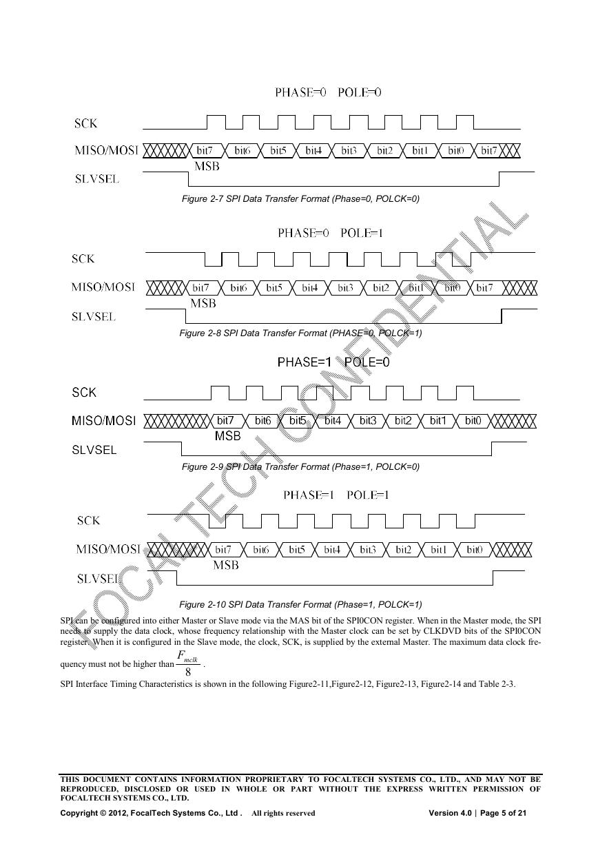
SPI transfers data at 8bit packets. The phase relationship between the data and the clock can be defined by the two registers: phase and
polck. Some data transfer examples can be found in Figure 2-7 to Figure 2-10.
THIS DOCUMENT CONTAINS INFORMATION PROPRIETARY TO FOCALTECH SYSTEMS CO., LTD., AND MAY NOT BE
REPRODUCED, DISCLOSED OR USED IN WHOLE OR PART WITHOUT THE EXPRESS WRITTEN PERMISSION OF
FOCALTECH SYSTEMS CO., LTD.
Copyright © 2012, FocalTech Systems Co., Ltd . All rights reserved Version 4.0︱Page 4 of 21
�
Figure 2-7 SPI Data Transfer Format (Phase=0, POLCK=0)
Figure 2-8 SPI Data Transfer Format (PHASE=0, POLCK=1)
Figure 2-9 SPI Data Transfer Format (Phase=1, POLCK=0)
Figure 2-10 SPI Data Transfer Format (Phase=1, POLCK=1)
SPI can be configured into either Master or Slave mode via the MAS bit of the SPI0CON register. When in the Master mode, the SPI
needs to supply the data clock, whose frequency relationship with the Master clock can be set by CLKDVD bits of the SPI0CON
register. When it is configured in the Slave mode, the clock, SCK, is supplied by the external Master. The maximum data clock fre-
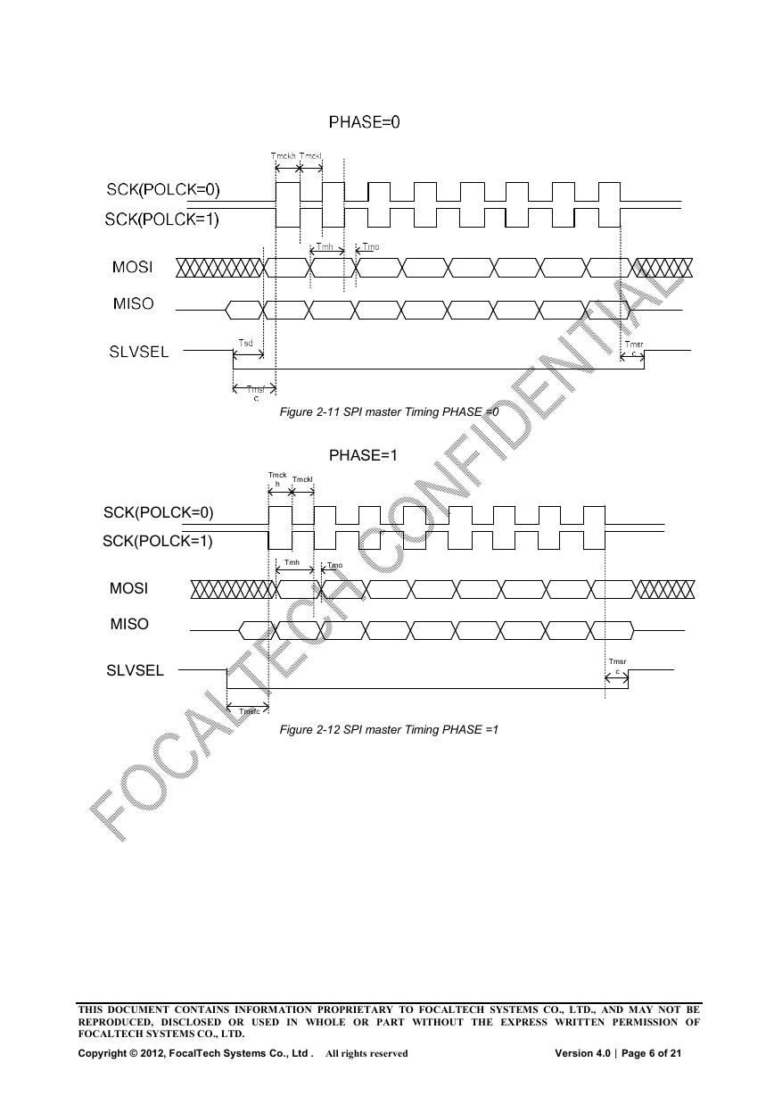
SPI Interface Timing Characteristics is shown in the following Figure2-11,Figure2-12, Figure2-13, Figure2-14 and Table 2-3.
quency must not be higher than
mclkF
8
.
THIS DOCUMENT CONTAINS INFORMATION PROPRIETARY TO FOCALTECH SYSTEMS CO., LTD., AND MAY NOT BE
REPRODUCED, DISCLOSED OR USED IN WHOLE OR PART WITHOUT THE EXPRESS WRITTEN PERMISSION OF
FOCALTECH SYSTEMS CO., LTD.
Copyright © 2012, FocalTech Systems Co., Ltd . All rights reserved Version 4.0︱Page 5 of 21
�
SCK(POLCK=0)
SCK(POLCK=1)
MOSI
MISO
SLVSEL
Figure 2-11 SPI master Timing PHASE =0
PHASE=1
Tmck
h
Tmckl
Tmh
Tmo
Tmsfc
Figure 2-12 SPI master Timing PHASE =1
Tmsr
c
THIS DOCUMENT CONTAINS INFORMATION PROPRIETARY TO FOCALTECH SYSTEMS CO., LTD., AND MAY NOT BE
REPRODUCED, DISCLOSED OR USED IN WHOLE OR PART WITHOUT THE EXPRESS WRITTEN PERMISSION OF
FOCALTECH SYSTEMS CO., LTD.
Copyright © 2012, FocalTech Systems Co., Ltd . All rights reserved Version 4.0︱Page 6 of 21
�


 V2版本原理图(Capacitive-Fingerprint-Reader-Schematic_V2).pdf
 摄像头工作原理.doc
 VL53L0X简要说明(En.FLVL53L00216).pdf
 原理图(DVK720-Schematic).pdf
 原理图(Pico-Clock-Green-Schdoc).pdf
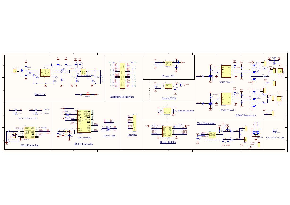 原理图(RS485-CAN-HAT-B-schematic).pdf
 File:SIM7500_SIM7600_SIM7800 Series_SSL_Application Note_V2.00.pdf
 ADS1263(Ads1262).pdf
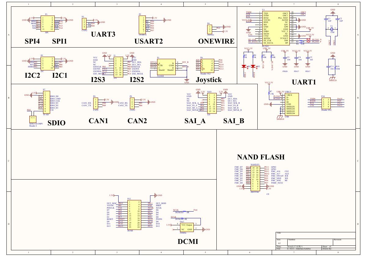 原理图(Open429Z-D-Schematic).pdf
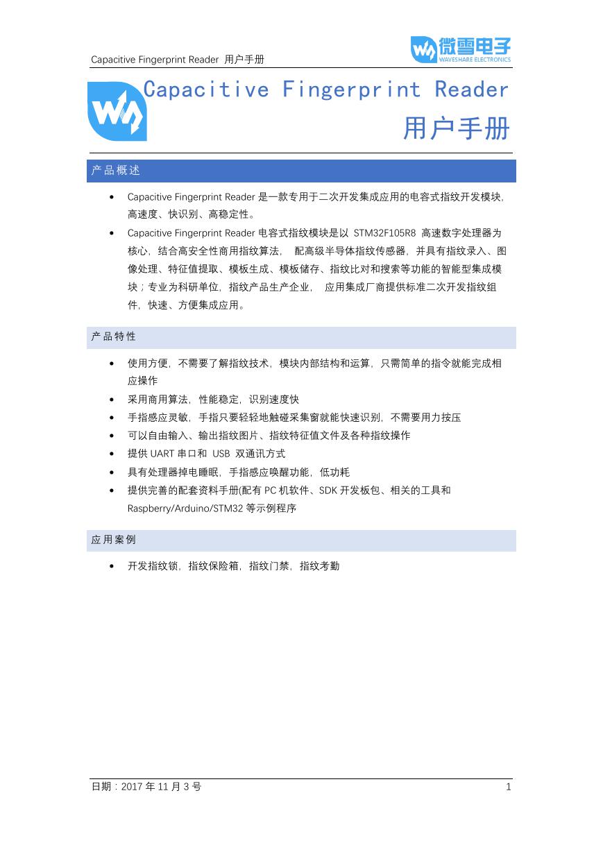 用户手册(Capacitive_Fingerprint_Reader_User_Manual_CN).pdf
 CY7C68013A(英文版)(CY7C68013A).pdf
 TechnicalReference_Dem.pdf