High Performance Four Channels Audio ADC
APPLICATIONS
ES7210
FEATURES
• High performance multi-bit delta-sigma
audio ADC
-85 dB THD+N
• 102 dB signal to noise ratio
•
• 24-bit, 8 to 100 kHz sampling frequency
I2S/PCM master or slave serial data port
•
• Support TDM
• 256/384Fs, USB 12/24 MHz and other
•
non standard audio system clocks
Low power standby mode
• Mic array
• Smart speaker
• Far field voice capture
ORDERING INFORMATION
ES7210 -40°C ~ +85°C
QFN-32
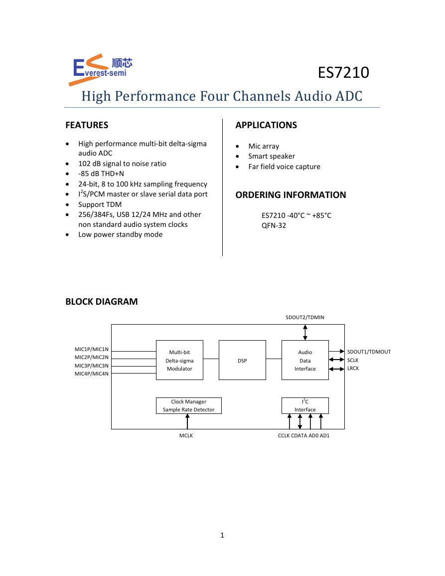
BLOCK DIAGRAM
MIC1P/MIC1N
MIC2P/MIC2N
MIC3P/MIC3N
MIC4P/MIC4N
DSP
Multi-bit
Delta-sigma
Modulator
Clock Manager
Sample Rate Detector
SDOUT2/TDMIN
Audio
Data
Interface
I2C
Interface
MCLK
CCLK CDATA AD0 AD1
SDOUT1/TDMOUT
SCLK
LRCK
1
�
Everest Semiconductor
Confidential
ES7210
1. PIN OUT AND DESCRIPTION
Pin Name
CDATA, CCLK
AD0, AD1
MCLK
SCLK
LRCK
SDOUT1/TDMOUT
SDOUT2/TDMIN
INT
DMIC_CLK
MIC1P, MIC1N
MIC2P, MIC2N
MIC3P, MIC3N
MIC4P, MIC4N
MICBIAS12
MICBIAS34
VDDP
VDDD, GNDD
VDDA, GNDA
VDDM
REFP12, REFP34
REFQ12, REFQ34
REFQM
Revision 19.0
R
E
F
Q
3
4
R
E
F
P
3
4
I
M
C
3
P
I
M
C
4
P
I
M
C
4
N
I
M
C
B
A
S
3
4
I
R
E
F
Q
M
I
M
C
3
N
1
2
3
4
5
6
7
8
AD0
AD1
CDATA
CCLK
MCLK
VDDP
VDDD
GNDD
3
2
3
1
3
0
2
9
2
8
2
7
2
6
2
5
ES7210
1
0
1
1
1
2
1
3
1
4
1
5
1
6
9
I
M
C
1
N
I
M
C
1
P
I
N
T
I
D
M
C
_
C
L
K
S
C
L
K
L
R
C
K
S
D
O
U
T
2
/
T
D
M
N
I
S
D
O
U
T
1
/
T
D
M
O
U
T
24
23
22
21
20
19
18
17
MICBIAS12
VDDM
VDDA
GNDA
MIC2N
MIC2P
REFQ12
REFP12
Pin number
3, 4
1, 2
5
9
10
11
12
13
14
16, 15
19, 20
31, 32
28, 27
24
26
6
7, 8
22, 21
23
17, 29
18, 30
25
Input or Output
I/O, I
I
I
I/O
I/O
O
I/O
O
O
Analog
Analog
Analog
Analog
Analog
Analog
Analog
Analog
Analog
Pin Description
I2C clock and data
I2C address
Master clock
Serial data bit clock
Serial data left and right channel frame clock
Serial data output or TDM data input and output
Interrupt
Digital mic clock
Mic input
MIC1P and MIC3P can be used as digital mic
data input
Mic bias
Power supply for the digital input and output
Digital power supply
Analog power supply
Analog power supply
Filtering capacitor connection
Filtering capacitor connection
Filtering capacitor connection
Latest datasheet: www.everest-semi.com or info@everest-semi.com
2
February 2022
�
Everest Semiconductor
Confidential
ES7210
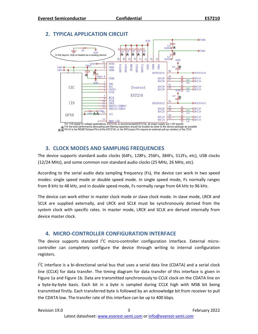
2. TYPICAL APPLICATION CIRCUIT
3. CLOCK MODES AND SAMPLING FREQUENCIES
The device supports standard audio clocks (64Fs, 128Fs, 256Fs, 384Fs, 512Fs, etc), USB clocks
(12/24 MHz), and some common non standard audio clocks (25 MHz, 26 MHz, etc).
According to the serial audio data sampling frequency (Fs), the device can work in two speed
modes: single speed mode or double speed mode. In single speed mode, Fs normally ranges
from 8 kHz to 48 kHz, and in double speed mode, Fs normally range from 64 kHz to 96 kHz.
The device can work either in master clock mode or slave clock mode. In slave mode, LRCK and
SCLK are supplied externally, and LRCK and SCLK must be synchronously derived from the
system clock with specific rates. In master mode, LRCK and SCLK are derived internally from
device master clock.
4. MICRO-CONTROLLER CONFIGURATION INTERFACE
The device supports standard I2C micro-controller configuration interface. External micro-
controller can completely configure the device through writing to internal configuration
registers.
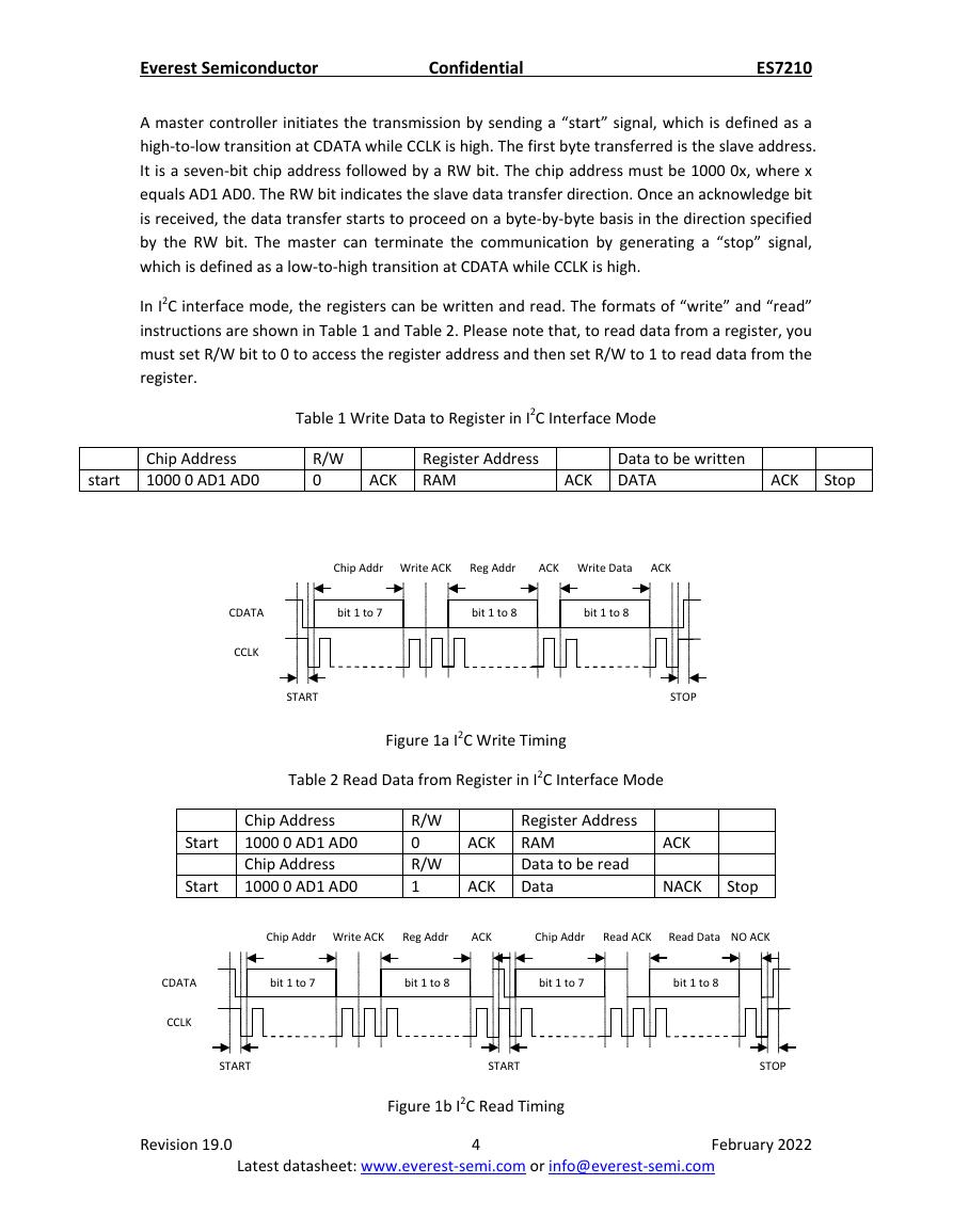
I2C interface is a bi-directional serial bus that uses a serial data line (CDATA) and a serial clock
line (CCLK) for data transfer. The timing diagram for data transfer of this interface is given in
Figure 1a and Figure 1b. Data are transmitted synchronously to CCLK clock on the CDATA line on
a byte-by-byte basis. Each bit in a byte is sampled during CCLK high with MSB bit being
transmitted firstly. Each transferred byte is followed by an acknowledge bit from receiver to pull
the CDATA low. The transfer rate of this interface can be up to 400 kbps.
Revision 19.0
Latest datasheet: www.everest-semi.com or info@everest-semi.com
3
February 2022
�
Everest Semiconductor
Confidential
ES7210
A master controller initiates the transmission by sending a “start” signal, which is defined as a
high-to-low transition at CDATA while CCLK is high. The first byte transferred is the slave address.
It is a seven-bit chip address followed by a RW bit. The chip address must be 1000 0x, where x
equals AD1 AD0. The RW bit indicates the slave data transfer direction. Once an acknowledge bit
is received, the data transfer starts to proceed on a byte-by-byte basis in the direction specified
by the RW bit. The master can terminate the communication by generating a “stop” signal,
which is defined as a low-to-high transition at CDATA while CCLK is high.
In I2C interface mode, the registers can be written and read. The formats of “write” and “read”
instructions are shown in Table 1 and Table 2. Please note that, to read data from a register, you
must set R/W bit to 0 to access the register address and then set R/W to 1 to read data from the
register.
Table 1 Write Data to Register in I2C Interface Mode
start
Chip Address
1000 0 AD1 AD0
R/W
0
ACK
Register Address
RAM
ACK
Data to be written
DATA
ACK
Stop
ACK
Write Data
ACK
bit 1 to 8
Chip Addr
Write ACK
bit 1 to 7
Reg Addr
bit 1 to 8
CDATA
CCLK
START
Figure 1a I2C Write Timing
Table 2 Read Data from Register in I2C Interface Mode
STOP
Start
Start
Chip Address
1000 0 AD1 AD0
Chip Address
1000 0 AD1 AD0
R/W
0
R/W
1
Register Address
RAM
Data to be read
Data
ACK
NACK
Stop
Chip Addr
Write ACK
Reg Addr
bit 1 to 7
bit 1 to 8
Chip Addr
Read ACK
Read Data
NO ACK
bit 1 to 7
bit 1 to 8
Figure 1b I2C Read Timing
Latest datasheet: www.everest-semi.com or info@everest-semi.com
STOP
February 2022
ACK
ACK
ACK
START
4
CDATA
CCLK
START
Revision 19.0
�
Everest Semiconductor
Confidential
ES7210
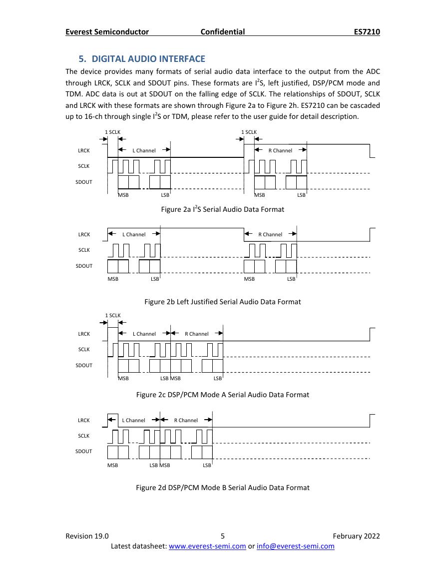
5. DIGITAL AUDIO INTERFACE
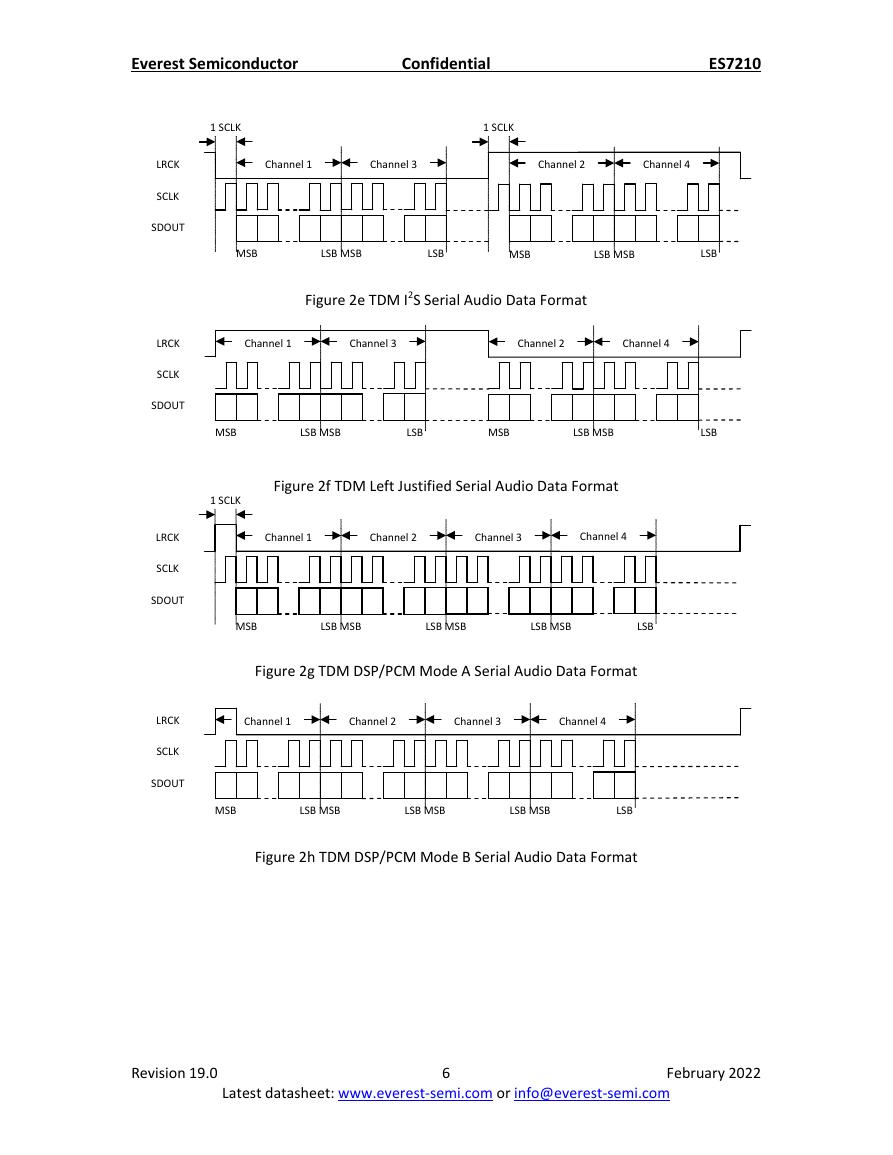
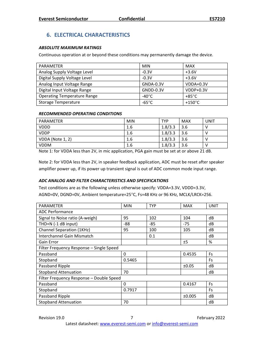
The device provides many formats of serial audio data interface to the output from the ADC
through LRCK, SCLK and SDOUT pins. These formats are I2S, left justified, DSP/PCM mode and
TDM. ADC data is out at SDOUT on the falling edge of SCLK. The relationships of SDOUT, SCLK
and LRCK with these formats are shown through Figure 2a to Figure 2h. ES7210 can be cascaded
up to 16-ch through single I2S or TDM, please refer to the user guide for detail description.
1 SCLK
R Channel
LSB
Figure 2a I2S Serial Audio Data Format
MSB
LSB
R Channel
MSB
LSB
Figure 2b Left Justified Serial Audio Data Format
1 SCLK
L Channel
MSB
L Channel
MSB
LSB
1 SCLK
LRCK
SCLK
SDOUT
LRCK
SCLK
SDOUT
LRCK
SCLK
SDOUT
LRCK
SCLK
SDOUT
Revision 19.0
L Channel
R Channel
MSB
LSB MSB
Figure 2c DSP/PCM Mode A Serial Audio Data Format
L Channel
R Channel
MSB
LSB MSB
LSB
Figure 2d DSP/PCM Mode B Serial Audio Data Format
LSB
5
Latest datasheet: www.everest-semi.com or info@everest-semi.com
February 2022
�
Everest Semiconductor
Confidential
ES7210
1 SCLK
Channel 1
Channel 3
MSB
LSB MSB
LSB
1 SCLK
Channel 2
Channel 4
MSB
LSB MSB
LSB
Figure 2e TDM I2S Serial Audio Data Format
LRCK
SCLK
SDOUT
LRCK
SCLK
SDOUT
LRCK
SCLK
SDOUT
LRCK
SCLK
SDOUT
LSB
Channel 1
Channel 3
MSB
LSB MSB
LSB
Channel 2
Channel 4
MSB
LSB MSB
Figure 2f TDM Left Justified Serial Audio Data Format
1 SCLK
Channel 1
Channel 2
Channel 3
Channel 4
MSB
LSB MSB
LSB MSB
LSB MSB
LSB
Figure 2g TDM DSP/PCM Mode A Serial Audio Data Format
Channel 1
Channel 2
MSB
LSB MSB
LSB MSB
Channel 3
Channel 4
LSB MSB
LSB
Figure 2h TDM DSP/PCM Mode B Serial Audio Data Format
Revision 19.0
Latest datasheet: www.everest-semi.com or info@everest-semi.com
6
February 2022
�
Everest Semiconductor
Confidential
ES7210
6. ELECTRICAL CHARACTERISTICS
ABSOLUTE MAXIMUM RATINGS
Continuous operation at or beyond these conditions may permanently damage the device.
PARAMETER
Analog Supply Voltage Level
Digital Supply Voltage Level
Analog Input Voltage Range
Digital Input Voltage Range
Operating Temperature Range
Storage Temperature
MIN
-0.3V
-0.3V
GNDA-0.3V
GNDD-0.3V
-40°C
-65°C
MAX
+3.6V
+3.6V
VDDA+0.3V
VDDP+0.3V
+85°C
+150°C
RECOMMENDED OPERATING CONDITIONS
PARAMETER
VDDD
VDDP
VDDA (Note 1, 2)
VDDM
Note 1: for VDDA less than 2V, in mic application, PGA gain must be set at or above 21 dB.
TYP
1.8/3.3
1.8/3.3
1.8/3.3
1.8/3.3
MAX
3.6
3.6
3.6
3.6
MIN
1.6
1.6
1.6
1.6
UNIT
V
V
V
V
Note 2: for VDDA less than 2V, in speaker feedback application, ADC must be reset after speaker
amplifier power up, if its power up transient signal is out of ADC common mode input range.
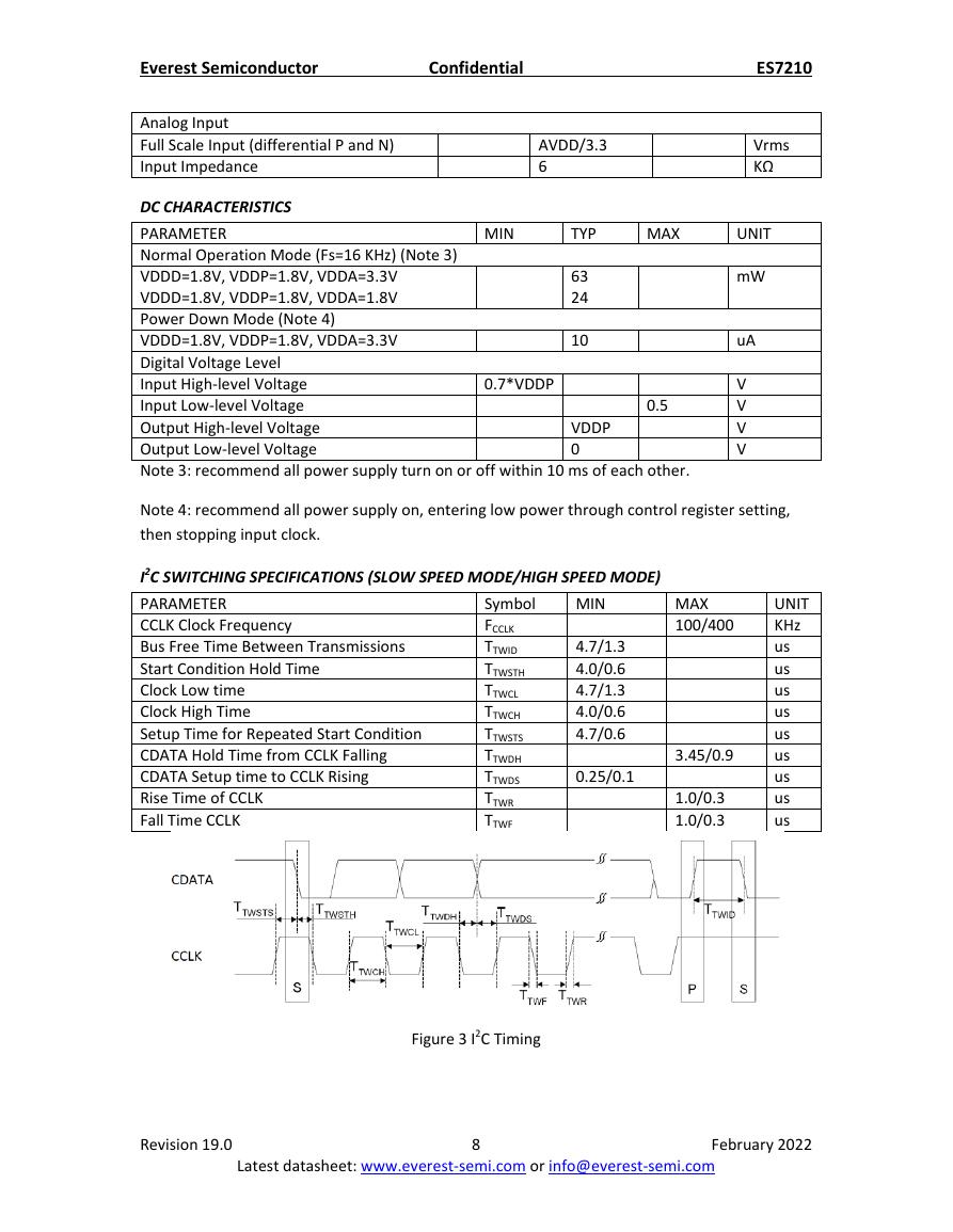
ADC ANALOG AND FILTER CHARACTERISTICS AND SPECIFICATIONS
Test conditions are as the following unless otherwise specify: VDDA=3.3V, VDDD=3.3V,
AGND=0V, DGND=0V, Ambient temperature=25°C, Fs=48 KHz or 96 KHz, MCLK/LRCK=256.
PARAMETER
ADC Performance
Signal to Noise ratio (A-weigh)
THD+N (-1 dB input)
Channel Separation (1KHz)
Interchannel Gain Mismatch
Gain Error
Filter Frequency Response – Single Speed
Passband
Stopband
Passband Ripple
Stopband Attenuation
Filter Frequency Response – Double Speed
Passband
Stopband
Passband Ripple
Stopband Attenuation
MIN
95
-88
95
0
0.5465
70
0
0.7917
70
TYP
102
-85
100
0.1
MAX
UNIT
104
-75
105
±5
0.4535
±0.05
0.4167
±0.005
dB
dB
dB
dB
%
Fs
Fs
dB
dB
Fs
Fs
dB
dB
Revision 19.0
Latest datasheet: www.everest-semi.com or info@everest-semi.com
7
February 2022
�
Everest Semiconductor
Confidential
ES7210
Analog Input
Full Scale Input (differential P and N)
Input Impedance
AVDD/3.3
6
Vrms
KΩ
MIN
TYP
MAX
DC CHARACTERISTICS
PARAMETER
Normal Operation Mode (Fs=16 KHz) (Note 3)
VDDD=1.8V, VDDP=1.8V, VDDA=3.3V
VDDD=1.8V, VDDP=1.8V, VDDA=1.8V
Power Down Mode (Note 4)
VDDD=1.8V, VDDP=1.8V, VDDA=3.3V
Digital Voltage Level
Input High-level Voltage
Input Low-level Voltage
Output High-level Voltage
Output Low-level Voltage
Note 3: recommend all power supply turn on or off within 10 ms of each other.
0.7*VDDP
VDDP
0
0.5
63
24
10
UNIT
mW
uA
V
V
V
V
Note 4: recommend all power supply on, entering low power through control register setting,
then stopping input clock.
I2C SWITCHING SPECIFICATIONS (SLOW SPEED MODE/HIGH SPEED MODE)
PARAMETER
CCLK Clock Frequency
Bus Free Time Between Transmissions
Start Condition Hold Time
Clock Low time
Clock High Time
Setup Time for Repeated Start Condition
CDATA Hold Time from CCLK Falling
CDATA Setup time to CCLK Rising
Rise Time of CCLK
Fall Time CCLK
MIN
4.7/1.3
4.0/0.6
4.7/1.3
4.0/0.6
4.7/0.6
0.25/0.1
Symbol
FCCLK
TTWID
TTWSTH
TTWCL
TTWCH
TTWSTS
TTWDH
TTWDS
TTWR
TTWF
MAX
100/400
3.45/0.9
1.0/0.3
1.0/0.3
UNIT
KHz
us
us
us
us
us
us
us
us
us
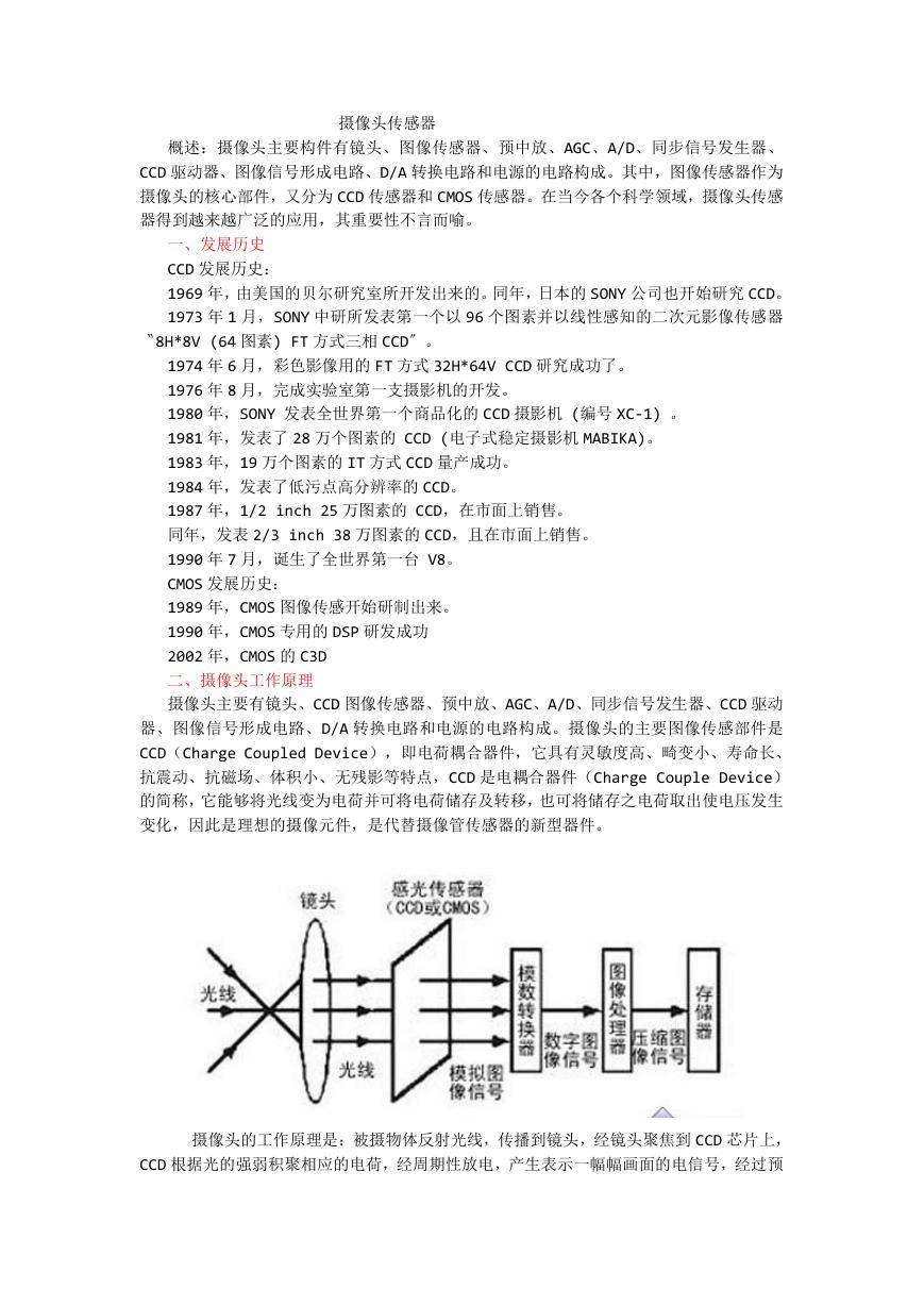
Figure 3 I2C Timing
Revision 19.0
Latest datasheet: www.everest-semi.com or info@everest-semi.com
8
February 2022
�



 V2版本原理图(Capacitive-Fingerprint-Reader-Schematic_V2).pdf
 摄像头工作原理.doc
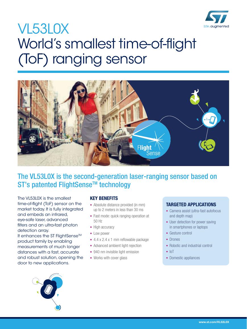 VL53L0X简要说明(En.FLVL53L00216).pdf
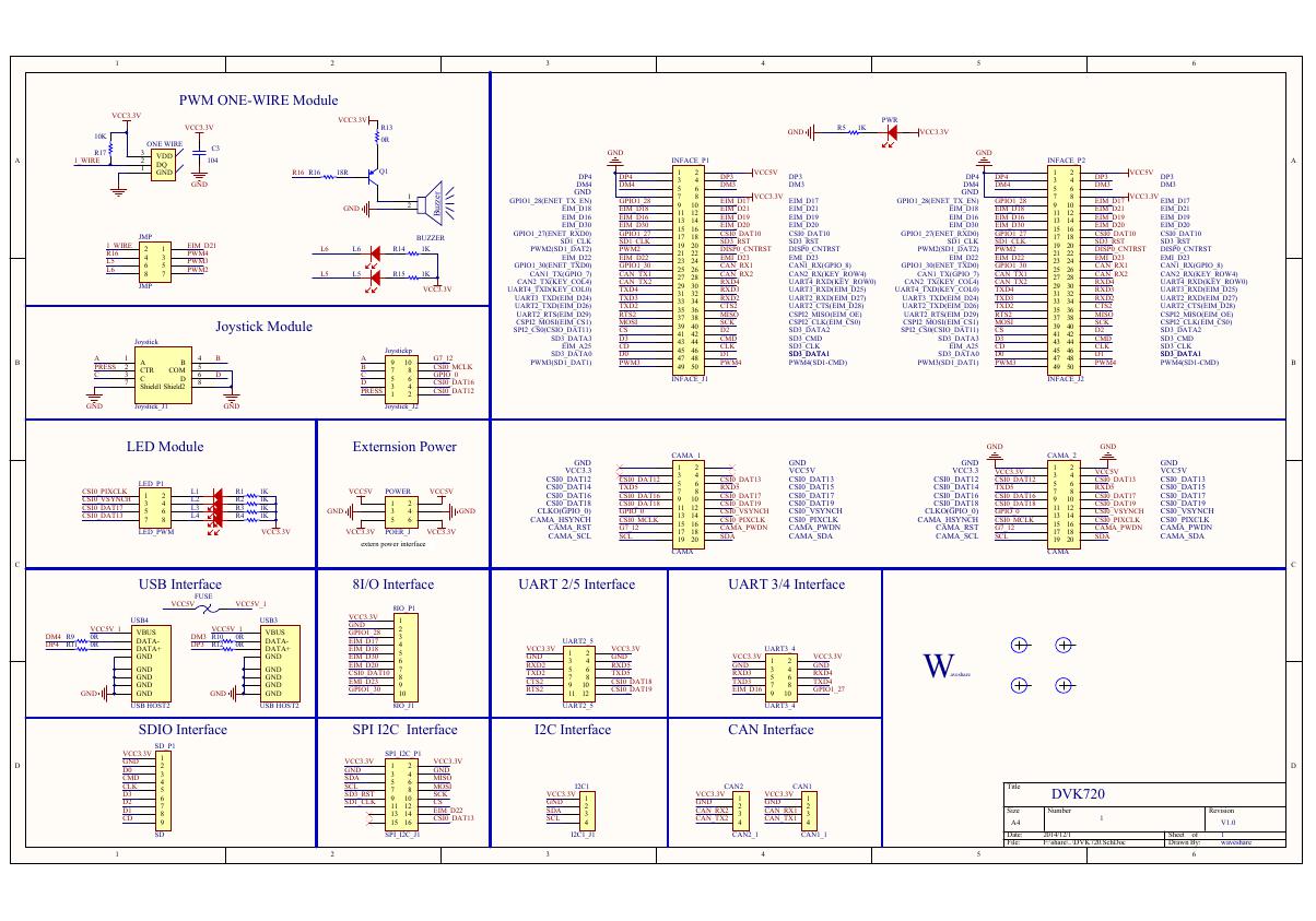 原理图(DVK720-Schematic).pdf
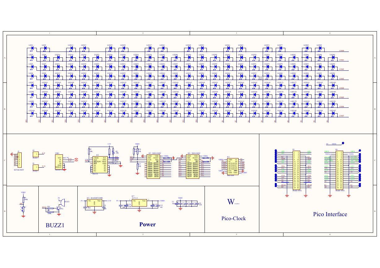 原理图(Pico-Clock-Green-Schdoc).pdf
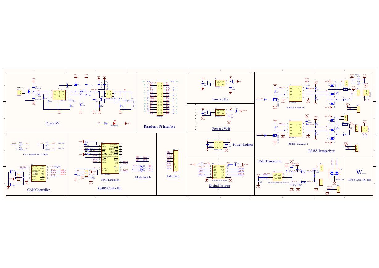 原理图(RS485-CAN-HAT-B-schematic).pdf
 File:SIM7500_SIM7600_SIM7800 Series_SSL_Application Note_V2.00.pdf
 ADS1263(Ads1262).pdf
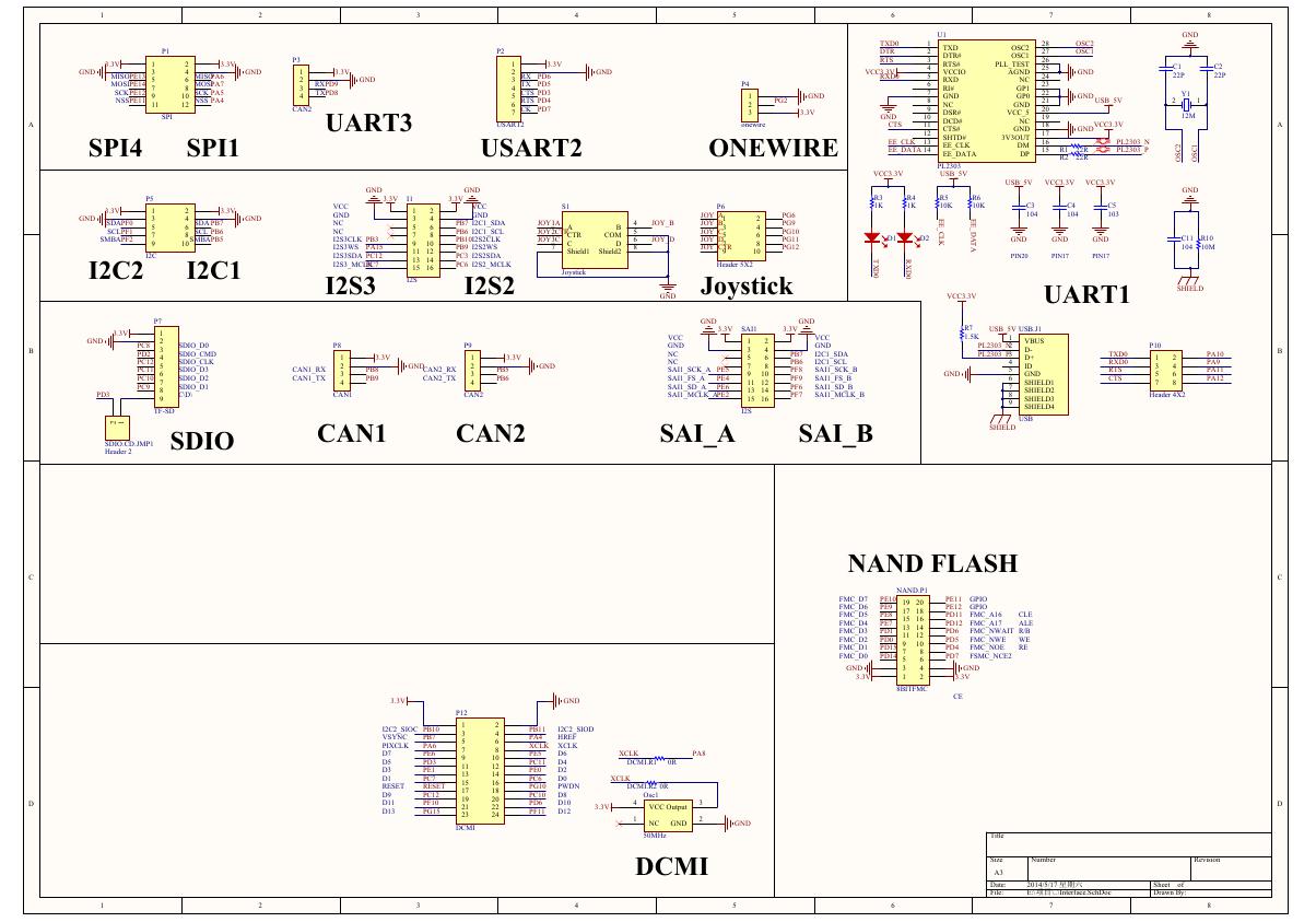 原理图(Open429Z-D-Schematic).pdf
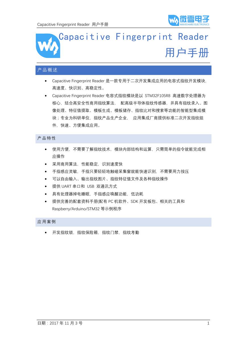 用户手册(Capacitive_Fingerprint_Reader_User_Manual_CN).pdf
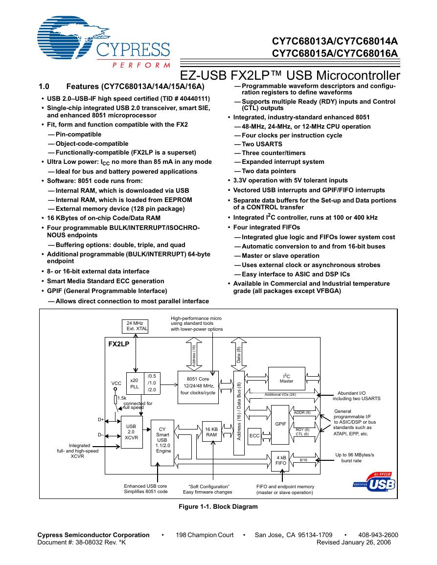 CY7C68013A(英文版)(CY7C68013A).pdf
 TechnicalReference_Dem.pdf