INTEGRATED CIRCUITS
DATA SHEET
PCF8591
8-bit A/D and D/A converter
Product specification
Supersedes data of 2001 Dec 13
2003 Jan 27
�
Product specification
PCF8591
Philips Semiconductors
8-bit A/D and D/A converter
CONTENTS
1
2
3
4
5
6
7
7.1
7.2
7.3
7.4
7.5
7.6
8
8.1
8.2
8.3
8.4
8.5
9
10
11
12
13
14
15
16
17
17.1
17.2
17.3
17.4
18
19
20
21
FEATURES
APPLICATIONS
GENERAL DESCRIPTION
ORDERING INFORMATION
BLOCK DIAGRAM
PINNING
FUNCTIONAL DESCRIPTION
Addressing
Control byte
D/A conversion
A/D conversion
Reference voltage
Oscillator
CHARACTERISTICS OF THE I2C-BUS
Bit transfer
Start and stop conditions
System configuration
Acknowledge
I2C-bus protocol
LIMITING VALUES
HANDLING
DC CHARACTERISTICS
D/A CHARACTERISTICS
A/D CHARACTERISTICS
AC CHARACTERISTICS
APPLICATION INFORMATION
PACKAGE OUTLINES
SOLDERING
Introduction to soldering through-hole mount
packages
Soldering by dipping or by solder wave
Manual soldering
Suitability of through-hole mount IC packages
for dipping and wave soldering methods
DATA SHEET STATUS
DEFINITIONS
DISCLAIMERS
PURCHASE OF PHILIPS I2C COMPONENTS
2003 Jan 27
2
�
Philips Semiconductors
8-bit A/D and D/A converter
FEATURES
1
• Single power supply
• Operating supply voltage 2.5 V to 6 V
• Low standby current
• Serial input/output via I2C-bus
• Address by 3 hardware address pins
• Sampling rate given by I2C-bus speed
• 4 analog inputs programmable as single-ended or
differential inputs
• Auto-incremented channel selection
• Analog voltage range from VSS to VDD
• On-chip track and hold circuit
• 8-bit successive approximation A/D conversion
• Multiplying DAC with one analog output.
2 APPLICATIONS
• Closed loop control systems
• Low power converter for remote data acquisition
• Battery operated equipment
• Acquisition of analog values in automotive, audio and
TV applications.
Product specification
PCF8591
3 GENERAL DESCRIPTION
The PCF8591 is a single-chip, single-supply low power
8-bit CMOS data acquisition device with four analog
inputs, one analog output and a serial I2C-bus interface.
Three address pins A0, A1 and A2 are used for
programming the hardware address, allowing the use of
up to eight devices connected to the I2C-bus without
additional hardware. Address, control and data to and from
the device are transferred serially via the two-line
bidirectional I2C-bus.
The functions of the device include analog input
multiplexing, on-chip track and hold function, 8-bit
analog-to-digital conversion and an 8-bit digital-to-analog
conversion. The maximum conversion rate is given by the
maximum speed of the I2C-bus.
4 ORDERING INFORMATION
TYPE
NUMBER
PCF8591P
PCF8591T
NAME
DIP16
SO16
PACKAGE
DESCRIPTION
plastic dual in-line package; 16 leads (300 mil)
plastic small outline package; 16 leads; body width 7.5 mm
VERSION
SOT38-4
SOT162-1
2003 Jan 27
3
�
Philips Semiconductors
8-bit A/D and D/A converter
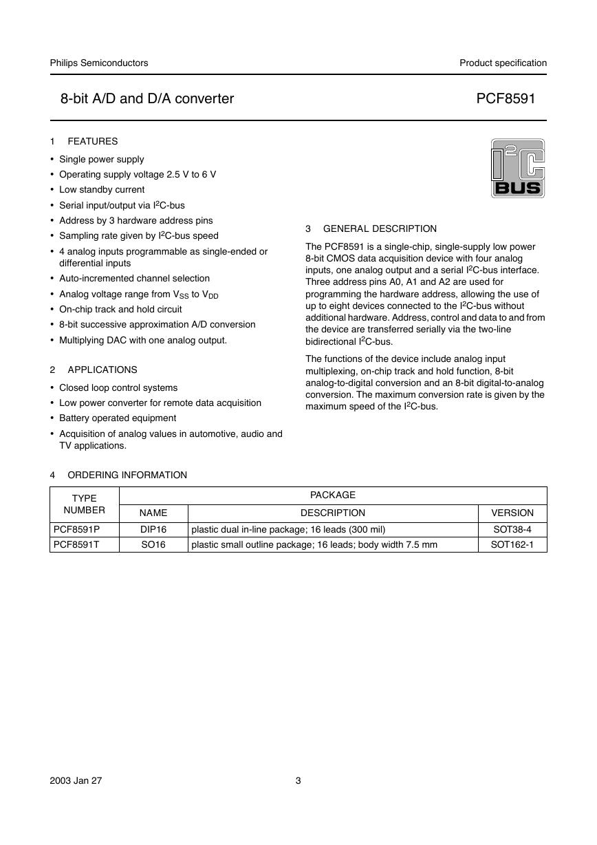
5 BLOCK DIAGRAM
handbook, full pagewidth
Product specification
PCF8591
I2C BUS
INTERFACE
POWER ON
RESET
ANALOGUE
MULTIPLEXER
SCL
SDA
A0
A1
A2
EXT
VDD
VSS
OSC
AIN0
AIN1
AIN2
AIN3
AOUT
PCF8591
STATUS
REGISTER
DAC DATA
REGISTER
ADC DATA
REGISTER
OSCILLATOR
CONTROL
LOGIC
SAMPLE
AND
HOLD
SAMPLE
AND
HOLD
COMPARATOR
SUCCESSIVE
APPROXIMATION
REGISTER/LOGIC
DAC
VREF
AGND
MBL821
Fig.1 Block diagram.
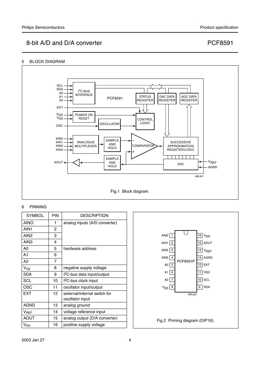
6 PINNING
SYMBOL
AINO
AIN1
AIN2
AIN3
A0
A1
A2
VSS
SDA
SCL
OSC
EXT
AGND
VREF
AOUT
VDD
PIN
1
2
3
4
5
6
7
8
9
10
11
12
13
14
15
16
DESCRIPTION
analog inputs (A/D converter)
hardware address
negative supply voltage
I2C-bus data input/output
I2C-bus clock input
oscillator input/output
external/internal switch for
oscillator input
analog ground
voltage reference input
analog output (D/A converter)
positive supply voltage
2003 Jan 27
4
handbook, halfpage
AIN0
AIN1
AIN2
AIN3
A0
A1
A2
VSS
1
2
3
4
5
6
7
8
16
VDD
15
AOUT
14
VREF
13
AGND
12
EXT
11
OSC
10
SCL
9
SDA
PCF8591P
MBL822
Fig.2 Pinning diagram (DIP16).
�
Philips Semiconductors
8-bit A/D and D/A converter
Product specification
PCF8591
handbook, halfpage
AIN0
AIN1
AIN2
AIN3
A0
A1
A2
VSS
1
2
3
4
5
6
7
8
16
VDD
15
AOUT
14
VREF
13
AGND
12
EXT
11
OSC
10
SCL
9
SDA
PCF8591T
MBL823
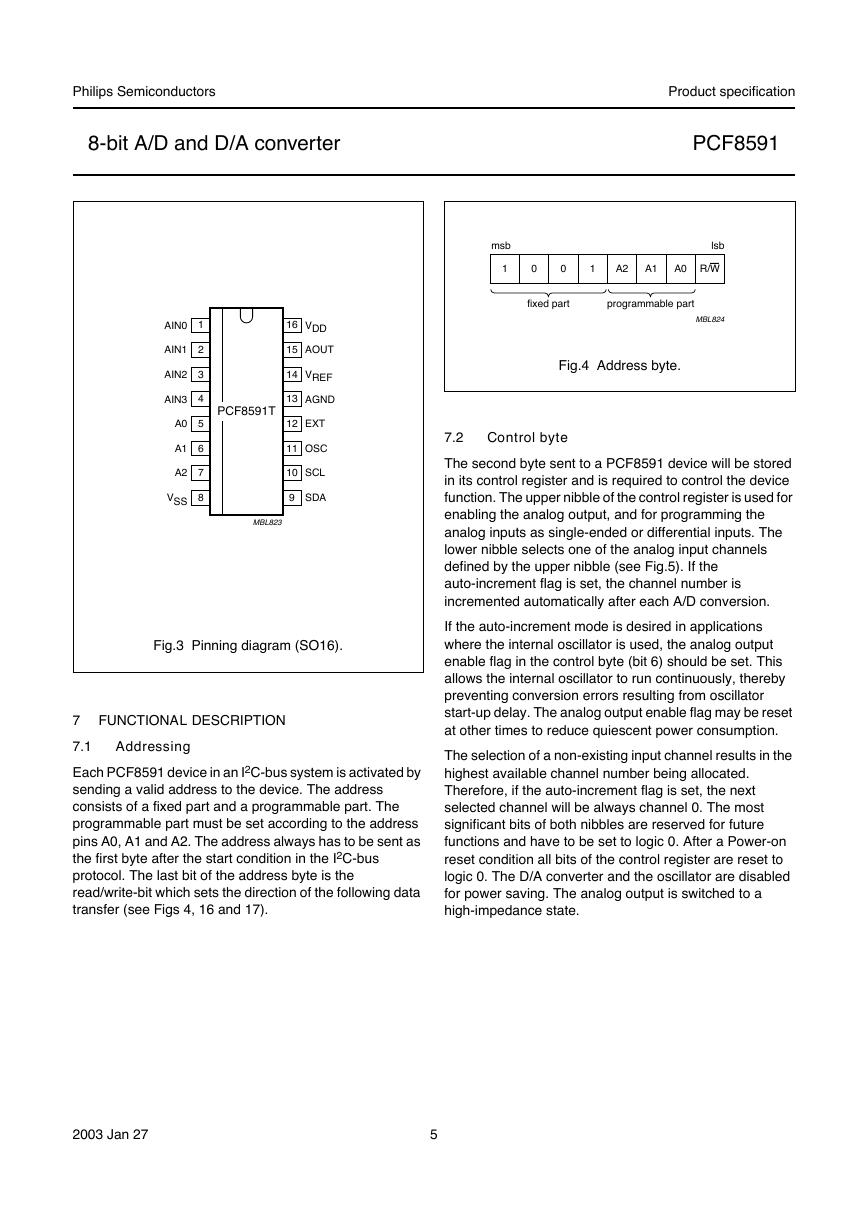
Fig.3 Pinning diagram (SO16).
7
FUNCTIONAL DESCRIPTION
7.1
Addressing
Each PCF8591 device in an I2C-bus system is activated by
sending a valid address to the device. The address
consists of a fixed part and a programmable part. The
programmable part must be set according to the address
pins A0, A1 and A2. The address always has to be sent as
the first byte after the start condition in the I2C-bus
protocol. The last bit of the address byte is the
read/write-bit which sets the direction of the following data
transfer (see Figs 4, 16 and 17).
handbook, halfpage
msb
lsb
1
0
0
1
A2
A1
A0 R/W
fixed part
programmable part
MBL824
Fig.4 Address byte.
7.2
Control byte
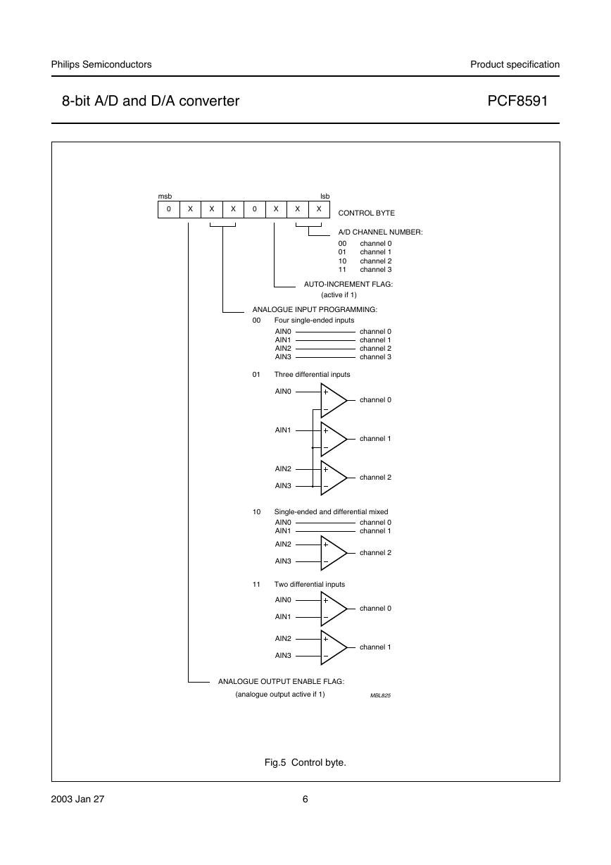
The second byte sent to a PCF8591 device will be stored
in its control register and is required to control the device
function. The upper nibble of the control register is used for
enabling the analog output, and for programming the
analog inputs as single-ended or differential inputs. The
lower nibble selects one of the analog input channels
defined by the upper nibble (see Fig.5). If the
auto-increment flag is set, the channel number is
incremented automatically after each A/D conversion.
If the auto-increment mode is desired in applications
where the internal oscillator is used, the analog output
enable flag in the control byte (bit 6) should be set. This
allows the internal oscillator to run continuously, thereby
preventing conversion errors resulting from oscillator
start-up delay. The analog output enable flag may be reset
at other times to reduce quiescent power consumption.
The selection of a non-existing input channel results in the
highest available channel number being allocated.
Therefore, if the auto-increment flag is set, the next
selected channel will be always channel 0. The most
significant bits of both nibbles are reserved for future
functions and have to be set to logic 0. After a Power-on
reset condition all bits of the control register are reset to
logic 0. The D/A converter and the oscillator are disabled
for power saving. The analog output is switched to a
high-impedance state.
2003 Jan 27
5
�
Philips Semiconductors
8-bit A/D and D/A converter
Product specification
PCF8591
handbook, full pagewidth
msb
lsb
0
X
X
X
0
X
X
X
CONTROL BYTE
A/D CHANNEL NUMBER:
00
01
10
11
channel 0
channel 1
channel 2
channel 3
AUTO-INCREMENT FLAG:
(active if 1)
ANALOGUE INPUT PROGRAMMING:
00
Four single-ended inputs
AIN0
AIN1
AIN2
AIN3
channel 0
channel 1
channel 2
channel 3
channel 0
channel 1
channel 2
01
Three differential inputs
AIN0
AIN1
AIN2
AIN3
10
Single-ended and differential mixed
channel 0
AIN0
AIN1
channel 1
AIN2
AIN3
11
Two differential inputs
AIN0
AIN1
AIN2
AIN3
channel 2
channel 0
channel 1
ANALOGUE OUTPUT ENABLE FLAG:
(analogue output active if 1)
MBL825
Fig.5 Control byte.
2003 Jan 27
6
�
Philips Semiconductors
8-bit A/D and D/A converter
Product specification
PCF8591
7.3
D/A conversion
The third byte sent to a PCF8591 device is stored in the
DAC data register and is converted to the corresponding
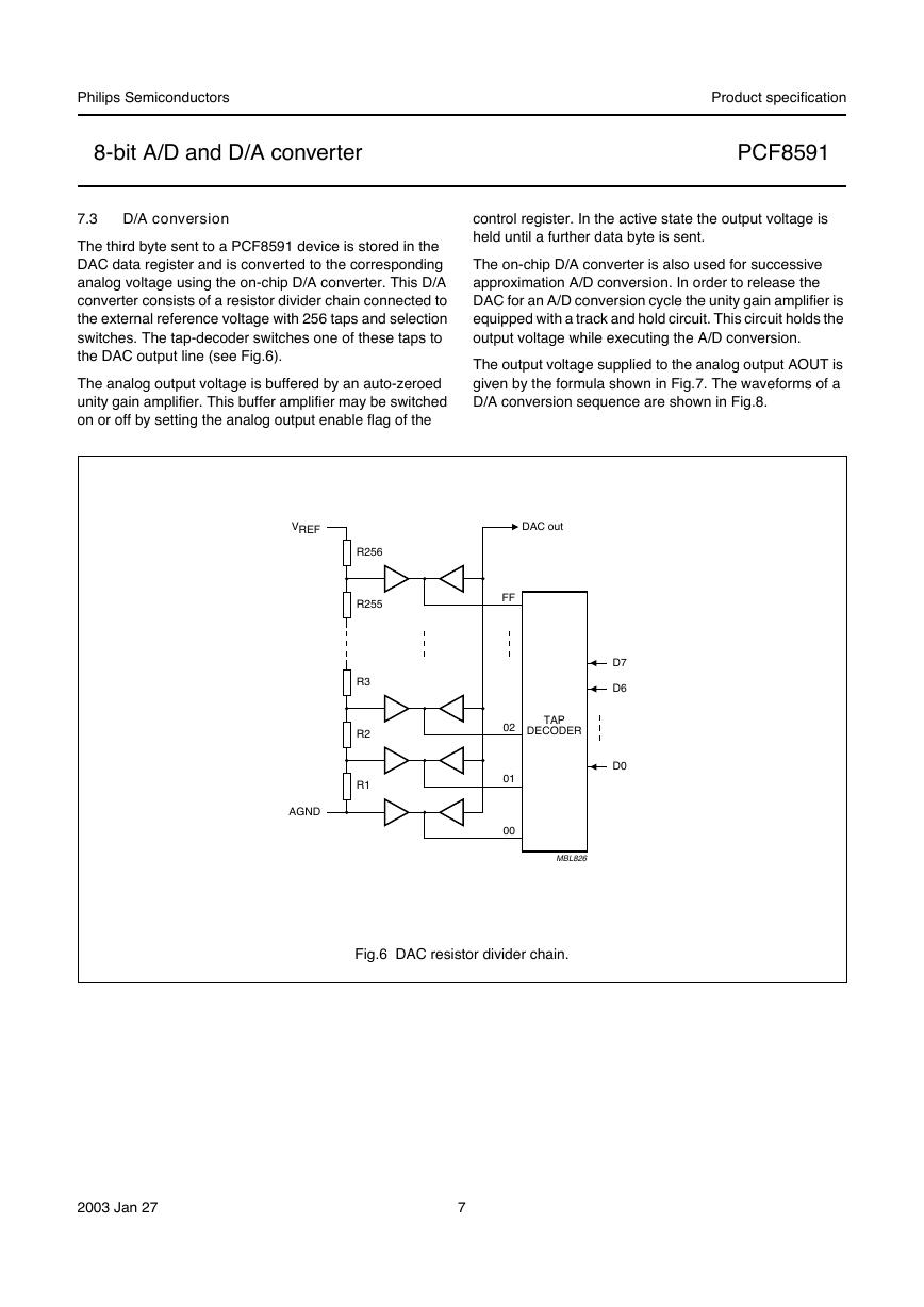
analog voltage using the on-chip D/A converter. This D/A
converter consists of a resistor divider chain connected to
the external reference voltage with 256 taps and selection
switches. The tap-decoder switches one of these taps to
the DAC output line (see Fig.6).
The analog output voltage is buffered by an auto-zeroed
unity gain amplifier. This buffer amplifier may be switched
on or off by setting the analog output enable flag of the
control register. In the active state the output voltage is
held until a further data byte is sent.
The on-chip D/A converter is also used for successive
approximation A/D conversion. In order to release the
DAC for an A/D conversion cycle the unity gain amplifier is
equipped with a track and hold circuit. This circuit holds the
output voltage while executing the A/D conversion.
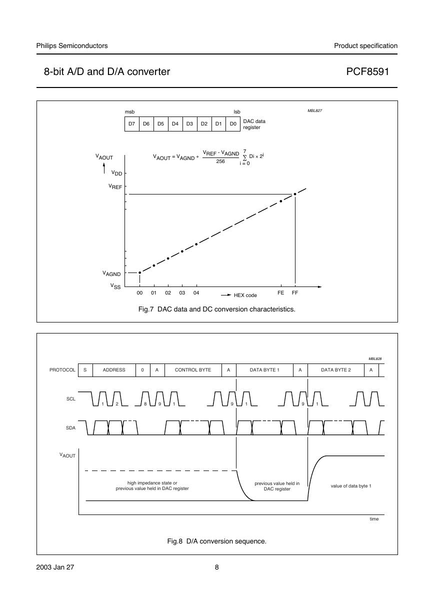
The output voltage supplied to the analog output AOUT is
given by the formula shown in Fig.7. The waveforms of a
D/A conversion sequence are shown in Fig.8.
handbook, full pagewidth
VREF
DAC out
R256
R255
R3
R2
R1
AGND
FF
02
TAP
DECODER
01
00
MBL826
D7
D6
D0
Fig.6 DAC resistor divider chain.
2003 Jan 27
7
�
Philips Semiconductors
8-bit A/D and D/A converter
Product specification
PCF8591
handbook, full pagewidth
msb
lsb
MBL827
D7
D6
D5
D4
D3
D2
D1
D0
DAC data
register
VAOUT
VAOUT = VAGND +
VREF - VAGND
7
Di · 2i
256
i = 0
VDD
VREF
VAGND
VSS
00
01
02
03
04
HEX code
FE
FF
Fig.7 DAC data and DC conversion characteristics.
handbook, full pagewidth
MBL828
PROTOCOL
S
ADDRESS
0
A
CONTROL BYTE
A
DATA BYTE 1
A
DATA BYTE 2
A
1
2
8
9
1
9
1
9
1
SCL
SDA
VAOUT
high impedance state or
previous value held in DAC register
previous value held in
DAC register
value of data byte 1
Fig.8 D/A conversion sequence.
time
2003 Jan 27
8
�



 V2版本原理图(Capacitive-Fingerprint-Reader-Schematic_V2).pdf
 摄像头工作原理.doc
 VL53L0X简要说明(En.FLVL53L00216).pdf
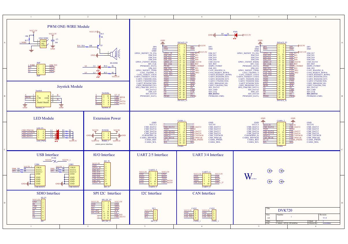 原理图(DVK720-Schematic).pdf
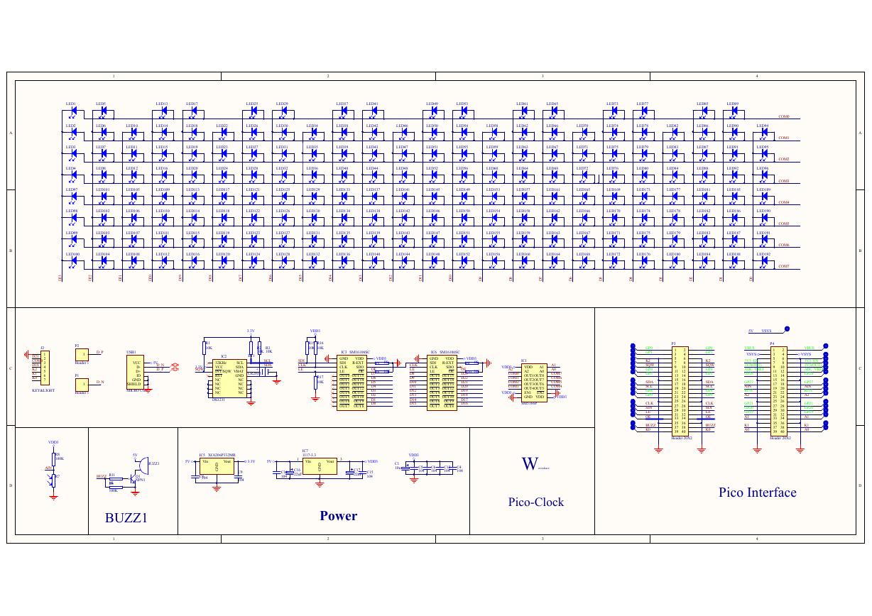 原理图(Pico-Clock-Green-Schdoc).pdf
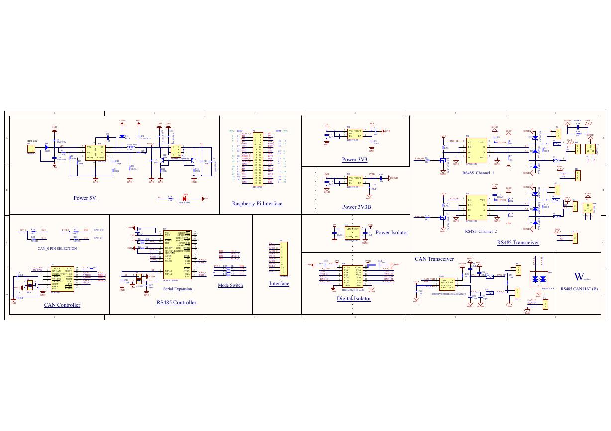 原理图(RS485-CAN-HAT-B-schematic).pdf
 File:SIM7500_SIM7600_SIM7800 Series_SSL_Application Note_V2.00.pdf
 ADS1263(Ads1262).pdf
 原理图(Open429Z-D-Schematic).pdf
 用户手册(Capacitive_Fingerprint_Reader_User_Manual_CN).pdf
 CY7C68013A(英文版)(CY7C68013A).pdf
 TechnicalReference_Dem.pdf